

МИНОБРНАУКИ РОССИИ
САНКТ-ПЕТЕРБУРГСКИЙ ГОСУДАРСТВЕННЫЙ
ЭЛЕКТРОТЕХНИЧЕСКИЙ УНИВЕРСИТЕТ
«ЛЭТИ» ИМ. В.И. УЛЬЯНОВА (ЛЕНИНА)
Кафедра МВЭ
Отчет по индивидуальному заданию №3
По дисциплине «Микроволновая электроника»
Студент гр. 9201 |
|
Рауан М. |
Преподаватель |
|
Иванов В.А. |
Санкт-Петербург
2022
Task 1.
Diodes with positive dynamic resistance.
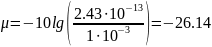
Given:
n = 2.45
Pmicro = 3.5 mV
T = 300 К
 Kl
Kl

Solution:
The conversion efficiency when operating at
direct current is evaluated by a parameter called current
sensitivity. The value of the
current sensitivity is equal to the ratio of the rectified current
increment
 to the value of the supplied microwave power
 :
:

To find
 we need to find
 ,
we can find it from previous formula:
,
we can find it from previous formula:
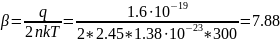
1.2

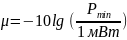
1.3 Given:
Teff=315 К
∆f=14 MHz

Find:
μ -?
Solution:

 Wt
Wt
Consequently:
 dBm
dBm
Describe the main similarities and differences in the functional role, structure, parameters of microwave devices with numbers:
Detector diode
Functional role: conversion of
energetically weak microwave signals ( )
W into a DC signal or isolation of the low-frequency envelope of this
signal in the presence of modulation.( Функциональная
роль: преобразование энергетически
слабых микроволновых сигналов
(〖10〗^(-6)÷〖10〗^(-2))
W
в сигнал постоянного тока или выделение
низкочастотной огибающей этого сигнала
при наличии модуляции.)
)
W into a DC signal or isolation of the low-frequency envelope of this
signal in the presence of modulation.( Функциональная
роль: преобразование энергетически
слабых микроволновых сигналов
(〖10〗^(-6)÷〖10〗^(-2))
W
в сигнал постоянного тока или выделение
низкочастотной огибающей этого сигнала
при наличии модуляции.)
Structures:
1) Point diode

Figure 1. point diode
As shown in the figure 1, the diode consists of a polycrystalline silicon sample p type 1, in contact with which there is a spring made of a pointed tungsten wire 2 at the end. The electrodes 3 and 4 are soldered to a ceramic housing 5. The tip of the spring is welded to the semiconductor by passing a current pulse. A very small Schottky barrier is formed at the welding site, which causes a small junction capacitance and a relatively high Rs value. such a structure is far from perfect, which leads to a deviation of its VAC from the ideal and the appearance of excessive noise. These disadvantages are absent in epitaxial structures with a sprayed metal film. (Как показано на рисунке 1, диод состоит из поликристаллического кремниевого образца p типа 1, в контакте с которым находится пружина, выполненная из заостренной вольфрамовой проволоки 2 на конце. Электроды 3 и 4 припаяны к керамическому корпусу 5. Наконечник пружины приваривается к полупроводнику путем пропускания импульса тока. В месте сварки образуется очень маленький барьер Шоттки, что приводит к небольшой емкости соединения и относительно высокому значению Rs. такая структура далека от совершенства, что приводит к отклонению ее VAC от идеального и появлению чрезмерного шума. Эти недостатки отсутствуют в эпитаксиальных структурах с напыленной металлической пленкой.)
2) Planar diode:
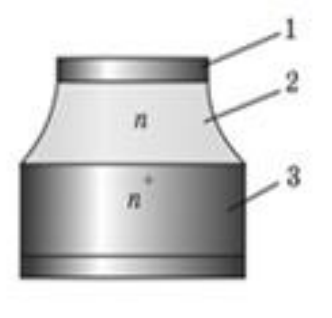
Fig.2. Planar diode.
These shortcomings are absent in epitaxial structures (Fig. 2). Such Schottky Barrier Diodes (SBD) is a gallium arsenide metha-structure. Metallization 1, deposited on a single crystal of gallium arsenide by vacuum evaporation, forms a Schottky barrier close to ideal with n-type epitaxial film 2. Highly alloyed n + substrate 3 produces low resistance Rs . Therefore, despite a greater capacitance as compared to a point diode, this SBD has higher critical frequency values at a lower noise level. (Эти недостатки отсутствуют в эпитаксиальных структурах (рис. 2). Такие барьерные диоды Шоттки (SBD) представляют собой метаструктуру арсенида галлия. Металлизация 1, нанесенная на монокристалл арсенида галлия вакуумным испарением, образует барьер Шоттки, близкий к идеальному, с эпитаксиальной пленкой 2 n-типа. Высоколегированная n + подложка 3 обеспечивает низкое сопротивление Rs. Поэтому, несмотря на большую емкость по сравнению с точечным диодом, этот SBD имеет более высокие значения критической частоты при более низком уровне шума.)

Fig. 3. shows the diode of a planar design used in integrated circuits. The barrier is formed at the contact point of the metal electrode with n-type semiconductor. Covering contacts with gold ensures work stability of such devices in time.
(На рис. 3. показан диод планарной конструкции, используемый в интегральных схемах. Барьер образуется в точке контакта металлического электрода с полупроводником n-типа. Покрытие контактов золотом обеспечивает стабильность работы таких устройств во времени.)
Parameters:
WAH

а)- on a linear scale б)- on a logarithmic scale
2. Current sensitivity:

3. Tangential sensitivity:
4. Noise
ratio:
 – шумовое отношение
5. Boundary frequency:

6. Total resistance: Z=R+jX.
Sources: materials for lecture 14 (part of the manual "Microwave solid-state devices"), Microwave electronics pdf.pdf
Mixing diode
Functional role: conversion of a microwave signal into an intermediate frequency signal. It is most widely used in heterodyne receiving devices.

Fig. 4. Section of the mixing diode structure
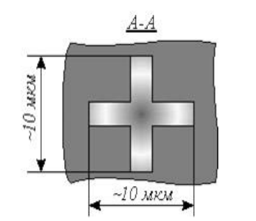
Fig. 5. Topology of the mixing diode
These devices use low—alloy semiconductors in the transition region, which are characterized by avalanche breakdown, mainly gallium arsenide, which helps to reduce the probability of breakdown. Changing the area of the structure on the one hand leads to a decrease in its capacity, and on the other hand — to an increase in its resistance. Thus, in order to achieve some optimal solution, the diode designs are made in the form of complex geometric shapes, in particular — in the form of a cross.( Рис. 5. Топология смесительного диода
В этих устройствах используются низколегированные полупроводники в переходной области, которые характеризуются лавинным пробоем, в основном арсенид галлия, что помогает снизить вероятность пробоя. Изменение площади конструкции, с одной стороны, приводит к уменьшению ее емкости, а с другой стороны — к увеличению ее сопротивления. Таким образом, для достижения некоторого оптимального решения конструкции диодов выполнены в виде сложных геометрических фигур, в частности — в виде креста.)
Parameters:
VAH: similar to D.
Noise ratio:

Boundary frequency:
Total resistance: Z=R+jX.
Describe circuit design models (not application schemes!) of microwave diodes with positive dynamic resistance (arbitrary choice) using available information sources Internet, lectures, AWR program Microwave Office, etc.

P-I-N diode

Fig. 6. Structure of p-i-n diode

Fig. 7. The concentration distribution of mobile carriers upon forward bias

Fig. 8. Design and equivalent circuits of the p-i-n diode

Fig. 9. Diode installed in microwave line.

Fig. 10. Limiter circuit operation: a — diode in waveguide; b — amplitude characteristic.