

Instrumentation Sensors Book
.pdfwww.globalautomation.info
3.4 Bridge Circuits |
|
35 |
|
A |
|
R1 |
R2 |
|
B |
D |
+ |
|
||
|
|
|
|
|
V |
|
|
− |
E |
|
|
R3 |
R4 |
|
|
C |
|
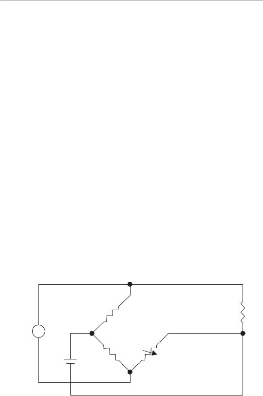
Figure 3.10 Circuit of a basic Wheatstone bridge.
in the form of a diamond with the supply and measuring instruments connected across the bridge as shown. When all the resistors are equal the bridge is balanced; that is, the bridge voltage at A and C are equal (E/2), and the voltmeter reads zero. Making one of the resistors a variable resistor the bridge can be balanced.
The voltage at point C referenced to D = E × R4/(R3 |
+ R4) |
|
The voltage at point A referenced to D = E × R2/(R1 |
+ R2) |
|
The voltage (V) between A and C = E R4/(R3 + R4) − E R2/(R1 + R2) |
(3.17) |
|
When the bridge is balanced V = 0, |
|
|
and R3R2 = R1R4 |
|
(3.18) |
It can be seen from (3.17) that if R1 is the resistance of a sensor whose change in value is being measured, the voltage at A will increase with respect to C as the resistance value decreases, so that the voltmeter will have a positive reading. The voltage
(V) will change in proportion to small changes in the value of R1, making the bridge very sensitive to small changes in resistance. Resistive sensors such as strain gauges are temperature sensitive and are often configured with two elements that can be used in a bridge circuit to compensate for changes in resistance due to temperature changes, for instance, if R1 and R2 are the same type of sensing element. Then resistance of each element will change by an equal percentage with temperature, so that the bridge will remain balanced when the temperature changes. If R1 is now used to sense a variable, the voltmeter will only sense the change in R1 due to the change in the variable, not the change due to temperature [8].
Example 3.6
Resistors R1 and R2 in the bridge circuit shown in Figure 3.9 are the strain gauge elements used in Example 3.5. Resistors R3 and R4 are fixed resistors, with values of 4.3 kW. The digital voltmeter is also the same meter. What is the minimum change in R1 that can be detected by the meter? Assume the supply E is 10V.
36 |
www.globalautomation.info |
Basic Electrical Components |
|
The voltage at point C will be 5.0V, because R3 = R4, and the voltage at C equals one-half of the supply voltage. The voltmeter can use the 0.1V range, because the offset is 0V, giving a resolution of 0.1 mV. The voltage that can be sensed at A is given by:
EAD = 10 × R2/(R1 + R2) = 5.00 + 0.0001V
R1 = (50,000/50,001) − 5,000Ω
R1 = −49,999
Resolution = 1Ω
This example shows the improved resolution obtained by using a bridge circuit over the voltage divider in Example 3.5.
Lead Compensation
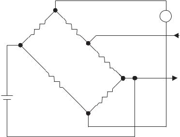
In many applications, the sensing resistor (R2) may be remote from a centrally located bridge. The resistance temperature device (RTD) described in Sections 10.3.2 and 15.3.4 is an example of such a device. In such cases, by using a two-lead connection as in Figure 3.10, adjusting the bridge resistor (R4) can zero out the resistance of the leads, but any change in lead resistance due to temperature will appear as a sensor value change. To correct this error, lead compensation can be used. This is achieved by using three interconnecting leads, labeled (a), (b), and (c) in Figure 3.11. A separate power lead (c) is used to supply R2. Consider point D of the bridge as now being at the junction of the supply and R2. The resistance of lead (b) is now a part of resistor R4 and the resistance of lead (a) is now a part of remote resistor R2. Since both leads have the same length with the same resistance and in the same environment, any changes in the resistance of the leads will cancel, keeping the bridge balanced.
|
|
A |
(a) |
|
|
|
|
|
|
|
R1 |
|
Remote sensor |
R2 |
|
|
|
||
+ |
B |
|
|
|
V |
|
|
|
|
|
|
|
|
|
− |
|
|
(b) |
D |
|
|
|
||
E |
R3 |
|
R4 |
|
|
|
|
|
|
|
|
|
C |
|
|
|
|
(c) |
|
Figure 3.11 Circuit of a Wheatstone bridge with compensation for lead resistance used in remote sensing.
3.4 Bridge Circuits |
www.globalautomation.info |
37 |
Current Balanced Bridge
A current feedback loop can be used to automatically null the Wheatstone bridge, as shown in Figure 3.12. A low-value resistor R5 is connected in series with resistor R2. The output from the bridge is amplified and converted into a current I, which is fed through R5 to develop an offset voltage, keeping the bridge balanced. The current through R5 can then be monitored to measure any changes in R2. The bridge is balanced electronically to give a fast response time, and there are no null potentiometers to wear out. Initially, when the bridge is at null with zero current from the feedback loop:
R3 (R2 + R5) = R1 × R4
assume R2 changes to R2 +  R2. Then, to rebalance the bridge;
R3 (R2 +  R2 + R5) − IR5 = R1 × R4
Subtracting the equations
δR2 = IR5/R3 |
(3.19) |
showing a linear relationship between changes in the sensing resistor and the feedback current, with R5 and R3 having fixed values.
Due to the two features of high sensitivity to small changes in resistance and correction for temperature effects, bridges are extensively used in instrumentation with strain gauges, piezoresistive elements, and magnetoresistive elements. The voltmeter should have a high resistance, so that it does not load the bridge circuit. Bridges also can be used with ac supply voltages and ac meters, not only for the
|
A |
+ |
|
|
|
|
|
V |
R1 |
R2 |
− |
B |
|
|
|
R5 |
I |
|
|
D |
R3
E
R4
C
Figure 3.12 Current balanced Wheatstone bridge.
38 |
www.globalautomation.info |
Basic Electrical Components |
|
measurement of resistance, but also for the measurement of capacitance, inductance, or a combination of resistance, capacitance, and inductance [9].
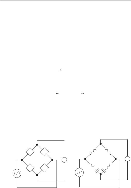
3.4.3ac Bridge Circuits
The basic concept of dc bridges can also be extended to ac bridges, the resistive elements are replaced with impedances, as shown in Figure 3.13(a). The bridge supply is now an ac voltage. This type of set up can be used to measure small changes in capacitance as required in the capacitive pressure sensor shown in Figure 7.5 in Chapter 7. The differential voltage  V across S is then given by:
δV = E |
Z2 Z3 − Z1 Z4 |
(3.20) |
|
(Z1 + Z3 )(Z2 + Z4 ) |
|
||
where E is the ac supply electromotive force (EMF). |
|
||
When the bridge is balanced, V = 0, and (3.20) reduces to: |
|
||
|
Z2Z3 = Z1Z4 |
(3.21) |
|
Or |
|
||
R2(R3 + j/ C1) = R1(R4 + J/ C2) |
|
||
Because the real and imaginary parts must be independently equal |
|
||
R3 × R2 = R1 × R4 |
(3.22) |
||
and |
|
||
R2 × C2 = R1 × C1 |
(3.23) |
||
|
|
A |
|
|
A |
|
Z1 |
Z2 |
|
R1 |
R2 |
|
|
|
|
||
|
B |
|
D |
B |
D |
|
|
S |
S |
||
|
|
|
|
||
|
|
|
|
|
|
E |
Z3 |
Z4 |
|
E |
|
|
R3 |
R |
|||
|
|
|
|
|
4 |
|
|
C |
|
C1 |
C2 |
|
|
|
|
C |
|
|
|
|
|
|
(a) |
(b) |
|
Figure 3.13 (a) An ac bridge using block impedances, and (b) a bridge with R and C components, as described in Example 3.7.
3.5 Summary www.globalautomation.info 39
Example 3.7
If the bridge circuit in Figure 3.13(b) is balanced, with R1 = 15 kΩ, R2 = 27 kΩ, R3 = 18 kΩ, and C1 = 220 pF, what are the values of R4 and C2?
R2R3 = R1R4
R4 = 27 × 18/15 = 32.4 kΩ
Additionally,
C2R2 = C1R1
C2 = 220 × 15/27 = 122 pF
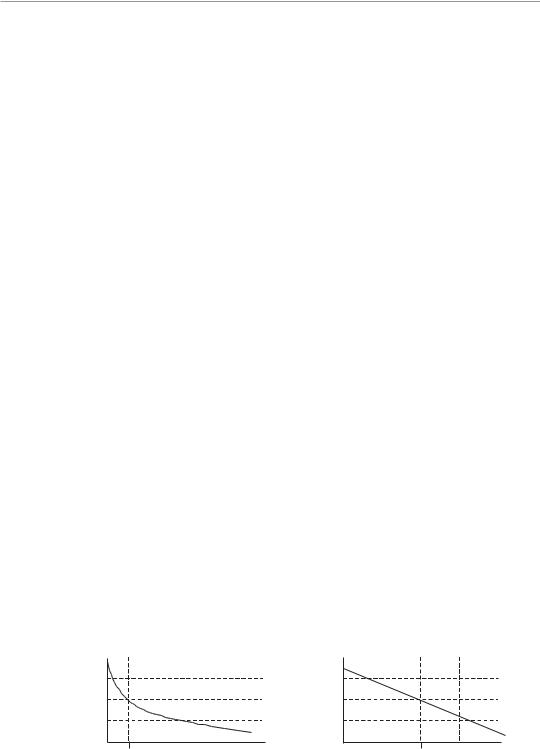
Bridge null voltage does not vary linearly with the amount the bridge is out of balance, as can be seen from (3.16). The variation is shown in Figure 3.14(a), so that ∆V should not be used to indicate out-of-balance unless a correction is applied. The optimum method is to use a feedback current to keep the bridge in balance, and measure the feedback current as in (3.19). Figure 3.14(b) shows that for an out-of-balance of less than 1%, the null voltage is approximately linear with ∆R.
3.5Summary
The effects of applying step voltages to passive components were discussed. When applying a step waveform to a capacitor or inductor, it is easily seen that the currents and voltages are 90° out of phase. Unlike in a resistor, these phase changes give rise to time delays that can be measured in terms of time constants. The phase changes also apply to circuits driven from ac voltages, and give rise to impedances, which can be combined with circuit resistance to calculate circuit characteristics and frequency dependency. Their frequency dependence makes them suitable for frequency selection and filtering.
It is required to measure small changes in resistance in many resistive sensors, such as strain gauges. The percentage change is small, making accurate measurement difficult. To overcome this problem, the Wheatstone Bridge circuit is used. By
volts |
+ |
volts |
0 |
||
∆V |
− |
∆V |
|
|
|
|
|
Null |
|
|
∆R Variations |
+
0
−
Null
∆R Variations
(a) |
(b) |
Figure 3.14 Bridge out-of-null voltage plotted against resistor variations, with (a) large variations, and (b) small variations.

|
www.globalautomation.info |
40 |
Basic Electrical Components |
comparing the resolution in a voltage divider and a bridge circuit, a large improvement in resolution of the bridge circuit can be seen. Bridge circuits also can be used for temperature compensation, compensation of temperature effects on leads in remote sensing, and with feedback for automatic measurement of resistive changes. The use of bridge networks also can be extended to measure changes in reactive components, as would be required in a capacitive sensor by the use of ac bridge configurations.
References
[1]Sutko, A., and J. D. Faulk, Industrial Instrumentation, 1st ed., Delmar Publishers, 1996, pp. 59–61.
[2]Bamble, S., “Demystifying Analog Filter Design,” Sensors Magazine, Vol. 19, No. 2, February 2002.
[3]Ramson, E., “An Introduction to Analog Filters,” Sensors Magazine, Vol. 18, No. 7, July 2001.
[4]Johnson, C. D., Process Control Instrumentation Technology, 7th ed., Prentice Hall, 2003,
pp.70–81.
[5]Humphries, J. T., and L. P. Sheets, Industrial Electronics, 4th ed., Delmar, 1993, pp. 7–11.
[6]Schuler, C. A., Electronics Principles and Applications, 5th ed., McGraw-Hill, 1999, pp. 243–245.
[7]Groggins, B., E. Jacobins, and C. Miranda, “Using an FPAA to Design a Multiple-Pole Filter for Low-g Sensing,” Sensors Magazine, Vol. 15, No. 2, February 1998.
[8]Anderson, K., “Looking Under the (Wheatstone) Bridge,” Sensors Magazine, Vol. 18, No. 6, June 2001.
[9]Johnson, C. D., Process Control Instrumentation Technology, 7th ed., Prentice Hall, 2003,
pp.58–69.

www.globalautomation.info
C H A P T E R 4
Analog Electronics
4.1Introduction
Process control electronic systems use both analog and digital circuits. The study of electronic circuits, where the input and output current and voltage amplitudes are continually varying, is known as analog electronics. In digital electronics, the voltage amplitudes are fixed at defined levels, such as 0V or 5V, which represent high and low levels, or “1”s and “0”s. This chapter deals with the analog portion of electronics.
In a process control system, transducers are normally used to convert physical process parameters into electrical signals, so that they can be amplified, conditioned, and transmitted to a remote controller for processing and eventual actuator control or direct actuator control. Measurable quantities are analog in nature; thus, sensor signals are usually analog signals. Consequently, in addition to understanding the operation of measuring and sensing devices, it is necessary to understand analog electronics, as applied to signal amplification, control circuits, and the transmission of electrical signals.
4.2Analog Circuits
The basic building block for analog signal amplification and conditioning in most industrial control systems is the operational amplifier (op-amp). Its versatility allows it to perform many of the varied functions required in analog process control applications.
4.2.1Operational Amplifier Introduction
Op-amps, because of their versatility and ease of use, are extensively used in industrial analog control applications. Their use can be divided into the following categories.
1.Instrumentation amplifiers are typically used to amplify low-level dc and low frequency ac signals (in the millivolt range) from transducers. These signals can have several volts of unwanted noise.
2.Comparators are used to compare low-level dc or low frequency ac signals, such as from a bridge circuit, or transducer signal and reference signal, to produce an error signal.
41

42 |
www.globalautomation.info |
Analog Electronics |
|
3.Summing amplifiers are used to combine two varying dc or ac signals.
4.Signal conditioning amplifiers are used to linearize transducer signals with the use of logarithmic amplifiers and to reference signals to a specific voltage or current level.
5.Impedance matching amplifiers are used to match the high output impedance of many transducers to the signal amplifier impedance, or amplifier output impedance to that of a transmission line.
6.Integrating and differentiating are used as waveform shaping circuits in low frequency ac circuits to modify signals in control applications.
4.2.2Basic Op-Amp
The integrated circuit (IC) made it possible to interconnect multiple active devices on a single chip to make an op-amp, such as the LM741/107 general-purpose op-amp. These amplifier circuits are small—one, two, or four can be encapsulated in a single plastic dual inline package (DIP) or similar package. The IC op-amp is a general purpose amplifier that has high gain and low dc drift, so that it can amplify dc as well as low frequency ac signals. When the inputs are at 0V, the output voltage is 0V, or can easily be adjusted to be 0V with the offset null adjustment. Op-amps require a minimal number of external components. Direct feedback is easy to apply, giving stable gain characteristics, and the output of one amplifier can be fed directly into the input of the next amplifier. Op-amps have dual inputs, one of which is a positive input (i.e., the output is in phase with the input), the other a negative input (i.e., the output is inverted from the input). Depending on the input used, these devices can have an inverted or a noninverted output, and can amplify differential sensor signals, or can be used to cancel electrical noise, which is often the requirement with low-level sensor signals. Op-amps are also available with dual outputs (i.e., both positive and negative). The specifications and operating characteristics of bipolar operational amplifiers, such as the LM 741/107 and MOS general purpose and high performance op-amps, can be found in semiconductor manufacturers’ catalogs [1].
4.2.3Op-Amp Characteristics
The typical op-amp has very high gain, high input impedance, low output impedance, low input offset, and low temperature drift. The parameters, although not ideal, give a good basic building block for signal amplification. Typical specifications from a manufacturer’s data sheets for a general-purpose integrated op-amp are as follows:
•Voltage gain, 200,000;
•Output impedance, 75Ω;
•Input impedance bipolar, 2 MΩ;
•Input impedance MOS, 1012 Ω;
•Input offset voltage, 5 mV;
•Input offset current, 200 nA.
These are just the basic parameters in several pages of specifications [2].
4.2 Analog Circuits |
www.globalautomation.info |
43 |
The very high gain of the basic amplifier is called the open loop gain, and is difficult to use, because vary small changes at the input to the amplifier (e.g., noise, drift due to temperature changes, and so forth) will cause the amplifier output to saturate. High gain amplifiers also tend to be unstable. The gain of the amplifier can be reduced using feedback, see Section 4.3.1, normally providing a stable fixed gain amplifier. This configuration is called the closed loop gain.
Input offset is due to the input stage of op-amps not being ideally balanced. The offset is due to leakage current, biasing current, and transistor mismatch, and is defined as follows.
1.Input offset voltage. The voltage that must be applied between the inputs to drive the output voltage to zero.
2.Input offset current. The input current required to drive the output voltage to zero.
3.Input bias current. Average of the two input currents required to drive the output voltage to zero.
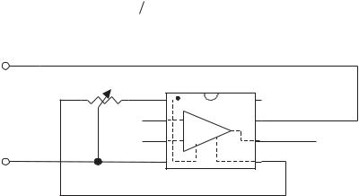
Op-amps require an offset control when amplifying small signals to null any differences in the inputs, so that the dc output of the amplifier is zero when the dc inputs are at the same voltage. In the case of the LM 741/107, provision is made to balance the inputs by adjusting the current through the input stages. This is achieved by connecting a 47k potentiometer between the offset null points, and taking the wiper to the negative supply line, as shown in Figure 4.1. Shown also are the pin numbers and connections (top view) for a DIP.
The ideal signal operating point for an op-amp is at one-half the supply voltage. The LM 741 is normally supplied from +15V and −15V (using a 30V supply), and the signals are referenced to ground [3].
Slew Rate (SR) is a measure of the op-amp’s ability to follow transient signals, and affects the amplifier’s large signal response. The slew rate is the rate of rise of the output voltage, expressed in millivolts per microsecond, when a step voltage is applied to the input. Typically, a slew rate may range from 500 to 50 mV/ s. The rate is determined by the internal and external capacitances and resistance. The slew rate is given by:
SR = ∆Vo ∆t |
(4.1) |
Positive
supply (+ 15 V)
Negative supply (−15 V)
Offset null |
|
Not connected |
|||
47 kΩ |
|
|
|||
|
|
|
|
||
Input − |
1 |
|
8 |
|
|
2 |
− |
7 |
|
||
Input + |
+ |
Output |
|||
|
|
||||
|
|
|
|||
|
3 |
6 |
|
||
|
|
Offset null |
|||
|
|
|
|
||
|
4 |
|
5 |
|
|
Figure 4.1 Offset control for the LM 741/107 op-amp.

44 |
www.globalautomation.info |
Analog Electronics |
|
where ∆Vo is the output voltage change, and ∆t is the time.
Unity gain frequency of an amplifier is the frequency at which the small signal open loop voltage gain is 1, d or a gain of 0 dB, which in Figure 4.2 is 1 MHz.
The bandwidth of the amplifier is defined as the point at which the small signal gain falls 3 dB. In Figure 4.2 and the open loop bandwidth is about 5 Hz, whereas the closed loop bandwidth is approximately 100 kHz, showing that feedback increases the bandwidth.
Gain bandwidth product (GBP) is similar to the slew rate, but is the relation between small signal open loop voltage gain and frequency. It can be seen that the small gain of an op-amp decreases with frequency, due to capacitances and resistances; capacitance is often added to improve stability. The gain versus frequency or Bode plot for a typical op-amp is shown in Figure 4.2. It can be seen from the graph that the GBP is a constant. The voltage gain of an op-amp decreases by 10 (20 dB) for every decade input frequency increase.
The GBP of an op-amp is given by:
GBP = BW × Av |
(4.2) |
where BW is the bandwidth and Av is the closed loop voltage gain of the amplifier.
Example 4.1
What is the bandwidth of the amplifier whose GBP is 1.5 MHz, if the voltage gain is 180?
|
120 |
|
|
|
|
|
|
|
100 |
|
|
|
|
|
|
(dB) |
80 |
|
|
|
|
|
|
|
|
|
|
|
|
|
|
gain |
60 |
|
|
Open loop characteristic |
|
||
|
|
|
|
|
|
||
Voltage |
40 |
|
|
|
|
|
|
|
|
|
|
|
|
|
|
|
|
Closed loop characteristic |
|
|
|
|
|
|
20 |
|
|
|
|
|
|
|
0 |
|
|
|
|
|
|
|
1 |
10 |
102 |
103 |
104 |
105 |
106 |
Frequency Hz
Figure 4.2 Typical frequency response or Bode plot of a compensated op-amp.