

Nanotechnology 24 (2013) 245502 |
C E Kehayias et al |
an electronically hybrid material that can be controllably tuned from an insulator to a semiconductor material via reduction chemistry [6, 19, 20]. Electrically conducting RGO platelets are typically obtained by exposing water-dispersed graphene oxide to different types of reducing agents, such as hydrazine [21], NaBH4 [22], and ascorbic acid [16]. The resulting RGO platelets are composed of carboxyl, alcohol, and dangling oxygen functional groups embedded within the familiar hexagonal lattice of carbon atoms [19]. The availability of these functional groups allows RGO to interact with a wide range of chemical analytes, which act as either electron-donors or electron-acceptors on the sample surface, thus leading to a significant change in the resistance of the RGO-based device [15, 16, 19, 23]. The RGO-based sensors are therefore amenable to chemical modifications that, in principle, permit one to control their chemical sensitivity and selectivity to a very high degree. However, despite recent rapid progress there are still several important challenges that need to be dealt with, before RGO-based devices can be employed as versatile chemical and biological sensors. For example, detailed quantitative understanding of the analyte-RGO charge transfer, of the spatial distribution of the resulting charge carriers, and of the role played by the contact resistance between the RGO sample and the metal electrodes are essential for an optimal device design.
Here we combine electronic transport with Kelvin probe microscopy (KPM) experiments to probe variations in the surface potential and local charge distribution for RGO-based electronic sensors exposed to two types of chemical compound: acetone (.CH3/2CO which acts as an electron acceptor) and ammonia (NH3, an electron donor). For these two analytes the variation of the device resistance and the induced charge are consistent with a chemical gating effect on the RGO conduction channel where hole conduction dominates. We quantify the amount of charge transferred to the sensor during chemical doping and spatially resolve the active sites of the sensor where the chemical gating process takes place. We also demonstrate that these experiments allow us to isolate the contributions from the contact resistance between the RGO and the metallic electrode, and show that the change in total resistance of our measured devices is mainly due to chemical doping of the RGO platelets.
2. Sample preparation and experimental setup
RGO platelets were prepared using a modified Hummers method, as described previously [16, 23]. Briefly, graphene oxide powder is obtained from graphite nanoplatelets via chemical treatment, and then further reduced using ascorbic acid (vitamin C) treatment. The resulting RGO powder is suspended in dimethyl formamide, and then a fine nanoplatelet suspension is obtained via sonication. X-ray photoelectron spectra (XPS) and thermogravimetric analysis (TGA) performed on similar RGO platelets [16] demonstrate that the vitamin C treatment is a mild and very effective alternative to hydrazine for reducing graphene oxide into RGO. To create assembly sites for the RGO platelets, Au electrodes were patterned on degenerately doped Si wafers
containing a 200 nm oxide layer using conventional sputtering techniques [23]. RGO-based field-effect transistors (RGOFETs) (figure 1(a)) were constructed by dielectrophoretic assembly of RGO platelets between the Au electrodes [23]. The RGO network between the source and drain electrodes serves as conducting channels for the device. Atomic force microscope (AFM) measurements show that the RGO platelets have a typical linear size of 0.5–1 m and a typical thickness of 20–50 nm. The gas sensing experiments for the RGO-FETs devices were performed at room temperature in a controlled environmental chamber [23]. Initially dry, clean air is used as a reference gas and directed over the device at a rate of 0.5 lpm. Analyte gases (acetone or NH3 at concentrations of 200 ppm [15, 16, 23]) are then sequentially substituted in the air flow (figure 1) with the total flow rate held constant. Some of the samples were also exposed to N2 flow at 0.5 lpm (instead of dry air). We find no significant difference between dry air and N2 for the sensing response of the device (supplementary figure 1 available at stacks.iop.org/ Nano/24/245502/mmedia).
3. Results and discussion
3.1. Electronic transport and sensor response to chemical doping
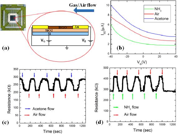
Figure 1(b) shows the variation of the source–drain current ISD with the gate voltage VG, for an RGO-FET device exposed to: dry air (red curve), acetone (blue curve) and NH3 (green curve). The source–drain bias voltage was VB D 1 V for all cases. The device shows p-dominated semiconducting behavior (i.e. hole conduction) over the whole range of applied gate voltages: 40 V VG 40 V.
The observed p-type behavior is consistent with previous results on RGO and graphene circuits obtained by chemical and thermal reduction of graphene oxide [15, 24, 25]. The threshold voltage of the device (defined as the minimum gate
voltage at which ISD is constant as a function of VG) when exposed to air is Vthair D 23 V. When the device is exposed
to acetone (an electron-withdrawing analyte [16, 23]) the
source–drain current increases over the applied VG scan range and the threshold voltage shifts to a larger value: Vthacetone D
28 V (blue curve in figure 1(b)). Conversely, when the same device is exposed to NH3 (an electron-donor analyte [15, 16]) we measure a decrease in ISD and a shift in the threshold voltage towards smaller values: VthNH3 D 16 V (green curve in figure 1(b)). These results demonstrate a charge transfer mechanism between the analyte (acetone or ammonia) and the RGO-FET sensor, where hole conduction dominates. NH3 acts as an electron donor upon adsorption onto RGO [15], and it is expected to lower the concentration of charge carriers (holes), therefore decreasing the on-state current and shifting the threshold voltage towards the negative regime. Acetone serves as an electron acceptor [16, 23], and it is therefore expected to increase the charge carrier concentration, which results in increased on-state currents and threshold voltages. Similar chemical doping mechanisms have previously been proposed for grapheneand RGO-based sensors [7, 8, 15, 17].
2
Nanotechnology 24 (2013) 245502 |
C E Kehayias et al |
Figure 1. (a) Schematics of the electronic transport and gas sensing setup. The RGO-sensing devices are patterned on SiO2/Si wafers in a field-effect transistor configuration (VB and VG are the bias and gate voltages, respectively). RGO platelets are deposited between Au electrodes and aligned using dielectrophoresis. Each sensing device can be successively exposed to dry air and analytes (acetone and ammonia at a concentration of 200 ppm). (b) Source–drain current ISD versus gate voltage VG for a device while continuously exposed to: dry air (red curve), acetone (blue curve) and ammonia (green curve). The applied bias voltage was VB D 1 V, and all gate sweeps were performed from 40 to C40 V at a rate of 0.5 V s 1. The device shows a p-type response in air and the response to the analytes is characteristic of a chemical gating mechanism. (c) Dynamic response (device resistance versus time) for the device measured in (b), when exposed successively to dry air (red arrows) and acetone (blue arrows). Five cycles are shown, demonstrating reversibility and fast response and recovery times (tens of seconds). The decrease in device resistance upon acetone exposure is about 25%. (d) Dynamic response for the device measured in (b) and (c), when exposed successively to dry air (red arrows) and ammonia (green arrows). Five cycles are shown, demonstrating reversibility and fast response and recovery times (tens of seconds). The increase in device resistance upon exposure to ammonia is about 45%. The applied bias voltage was VB D 1 V and the gate voltage was VG D 0 V for both (c) and (d).
The shifts of the ISD–VG transport curves in figure 1 can be used to calculate the relative change in the density of charge carriers for acetone (1na) and NH3 (j1nNH3 j) doping. Using e 1n D C 1Vth, where e is the electron charge, C is the SiO2 gate capacitance and 1Vth is the shift of the threshold voltage when the device is exposed to the analyte, measured relative to the threshold voltage when the device is exposed to air [15, 26], we obtain
1na |
|
|
Vthacetone Vthair |
|
|
j1nNH3 j |
D |
Vthair VthNH3 |
0:7: |
(1) |
|
In figures 1(c), (d) we show the dynamic response (device resistance versus time) for the RGO-FET sensor when exposed to analytes (acetone in figure 1(c), and NH3 in figure 1(d), respectively). The resistance of the sensor was measured for VB D 1 V and VG D 0 V first in air, then when the device was periodically exposed to analyte, and then air. The duration of each air (or analyte) exposure was
about 100 s. Five complete exposure cycles are shown in figure 1(c) (acetone) and figure 1(d) (NH3) to demonstrate the reproducibility and stability of the sensing response. Upon exposure to acetone the sensor resistance decreased by about 25% (figure 1(c)), while when the device was exposed to NH3 its resistance increased by about 45% (figure 1(d)). The sign of the dynamic response (decrease in device resistance for acetone, respectively increase in resistance for NH3) are again consistent with the expected chemical gating response for the electron-withdrawing acetone and the electron-donor NH3 vapors, which lead to an increase (decrease) in the concentration of charge carriers in the p-type RGO device. Figure 1(c) and d also show that the sensor response to the analytes and its recovery upon air exposure are rapid (tens of seconds) and reversible for the relatively low analyte vapor concentrations (200 ppm) studied here. We note that the overall sensing performance (response and recovery times, sensitivity and stability of the sensor) for these
3

Nanotechnology 24 (2013) 245502 |
C E Kehayias et al |
Figure 2. (a) AFM topographic image of an RGO-sensing device. The two Au electrodes (source and drain) and the RGO platelets are shown in the image. The RGO platelets are assembled in the central region, between the two electrodes. The RGO platelets have a typical linear size of 0.5–1 m and a typical thickness of 20–50 nm, as characterized by AFM. The red dotted square marks the region between the electrodes used for the KPM measurements shown in figures 3 and 4. This region is shown at higher resolution in the middle inset. The blue dotted lines in the inset mark the position of the Au electrodes. (b) Schematics of the Kelvin probe microscopy measurement, with overlapping RGO platelets assembled between the Au electrodes (see main text).
devices is at the level of the state of the art performance for graphene-based sensors reported in the literature [10, 15, 18]. This demonstrates that both the reduction method (based on vitamin C) and the dielectrophoretic assembly of RGO platelets are viable, high-throughput techniques for fabricating low-cost, high-sensitivity chemical sensors.
3.2. Kelvin probe microscopy of RGO devices
To gain a deeper quantitative understanding of the sensing mechanism we perform Kelvin probe microscopy (KPM) measurements of RGO devices both in air and upon exposure to acetone and NH3. KPM is a dual-pass AFM technique [27–29]. In the first line scan the AFM tip acquires the topography profile of the sample in tapping mode (figure 2(a)). In the second line scan, the tip travels at a preset height above the sample surface (h D 30 nm for the experiments presented here), as shown in figure 2(b). During the second pass the AFM cantilever is excited electrically by applying both a dc voltage Vdc, and an ac component with amplitude Vac D 1 V and frequency equal to the resonant frequency of the cantilever oscillation (!0 75 KHz, in our experiments). The dc component is controlled by a feedback loop such that the amplitude of the cantilever at !0 equals zero. Under these conditions the dc tip voltage Vdc matches the surface potential 8.x; y/ beneath the tip [27–29]. Thus by mapping Vdc versus the tip position, the KPM image records the distribution of the surface potential 8.x; y/ along the sample surface with very high spatial resolution (figures 3 and 4). Assuming that the work function of the tip and that of the charge-neutral RGO are constant, we have that Vdc directly tracks changes in the surface potential resulting from variations in the local charge carrier concentration. We note that a similar approach was used in [28] for mapping variations in the Fermi energy of charge-neutral single-layer graphene on SiC (0001) surfaces. For the measurements reported here KPM images were taken on an Asylum Research MFP3D AFM using platinum-coated tips with radius of curvature R D 20–30 nm, quality factor Q D 150 and spring constant k D 0:65–1 N m 1.
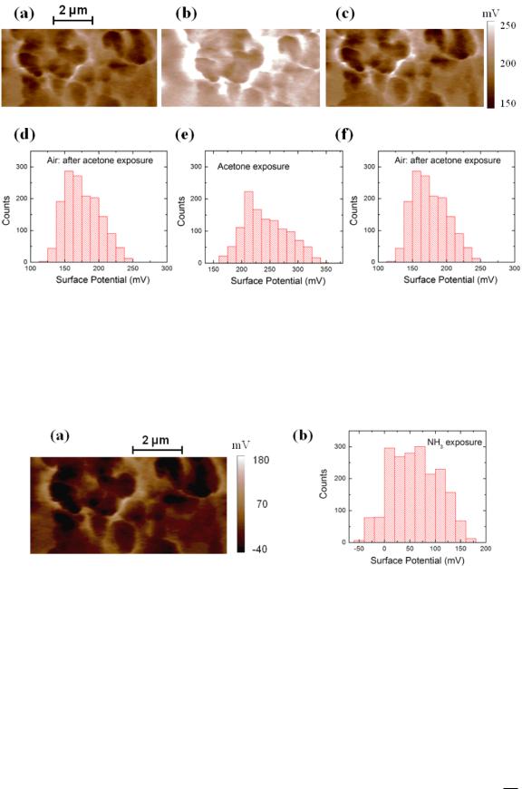
Figure 2 shows a typical AFM-topography image of a sample, including the two electrodes (figure 2(a)), and the schematics of the KPM setup (figure 2(b)). We have performed KPM measurements over the RGO regions between the two electrodes (indicated by the dotted red square, and shown as an inset in figure 2(a)), with the sample exposed to air (figure 3(a)), acetone (figure 3(b)) and then again to air (figure 3(c)). This sequence corresponds to a complete exposure cycle shown in transport data (figure 1(c)). The corresponding distributions in the surface potential are shown respectively in figures 3(d)–(f). The KPM data shows a clear shift in the average distribution of the surface potential upon exposure to acetone from Vair D .172:7 33/ mV (figure 3(d)) to Vacetone D .242 38/ mV (figure 3(e)). After exposure to acetone the sample is exposed again to air and the average of the surface potential distribution Vairafter D .176:2 25/ mV approaches the initial average of the distribution.
The chemical doping model implies that the observed shifts in the surface potential are due to charge transfer between the analyte (acetone) and the sample: vapor molecules of acetone adsorb near the sample surface, thus changing the electrostatic environment and increasing the concentration of hole charge carriers. This leads to an increased surface potential as measured by KPM. We note that the KPM images have very high spatial resolution and thus permit one to identify the regions of the sample where the chemical doping effect takes place, as well as the local changes in the surface potential due to charge transfer between the analyte and the RGO sample. For example, the comparison between figures 3(a) and (b) shows that the chemical doping is not uniform along the RGO surface, and also permits one to identify the gate-susceptible regions on the sensor surface (i.e. regions where the change in surface potential is maximum upon doping). To our knowledge these represent the first high-resolution measurements of charge transfer in RGO gas sensors.
3.3. Analysis of the combined Kelvin probe microscopy/electronic transport measurements
We combine the KPM and transport data to quantify the amount of charge transferred due to chemical doping, as
4
Nanotechnology 24 (2013) 245502 |
C E Kehayias et al |
Figure 3. (a)–(c) KPM potential maps of an RGO sensor when exposed to: dry air (a), acetone (b) and dry air (c). Figure (b) is taken while the acetone is applied (the sample was exposed to acetone for 15 min prior to the measurements, and then continuously exposed to acetone during the KPM experiments). Figure (c) is taken in dry air, and after the sample was continuously exposed to dry air for 15 min following the acetone exposure. The images show the variation in the surface potential due to gas exposure, and the active binding regions where chemical doping takes place. (d)–(f) Histograms of the surface potential for the images shown in (a)–(c), respectively. The average
values/standard deviations for these distributions are: Vair D .172:7 33/ mV, from (d), Vacetone D .242 38/ mV, from (e), and
Vairafter D .176:2 25/ mV, from (f) (the quoted experimental uncertainties are the standard deviations of the distributions). The distributions for the surface potential obtained during exposure to acetone are significantly different from the distributions obtained in air (p 0:05, one way ANOVA). These distributions are used to quantify the amount of charge transferred during chemical doping.
Figure 4. (a) KPM potential maps of an RGO sensor when exposed to ammonia. The image shows the variation in the surface potential due to gas exposure, and the active binding regions where chemical doping takes place. (b) Histogram of the surface potential for the image shown in (a). The average value/standard deviation for this distribution is VNH3 D .60 40/ mV, consistent with a decrease in the carrier charge density due to adsorption of the electron-donor ammonia vapors.
well as the contact resistance between the RGO and the Au electrodes. Assuming a negligible change in the total sample
capacitance C during acetone exposure we have C D Qair D
Vair
QairC1qa , where Qair D e A nair is the total electric charge when the device is exposed to air, and 1qa D e A 1na is the increase in the electric charge due to acetone exposure (here A is the sample surface area, while nair and 1na represent the density of charge carriers in air, and the increase in the density of charge carriers, respectively). From this expression it follows that: 1qa D Qair Vacetone Vair , or:
1na |
D |
Vacetone Vair : |
(2) |
|
nair |
Vair |
|
|
|
Equation (2) shows that the percentage change in the charge carrier density due to doping is equal to the percentage change in the surface potential measured by KPM. Using the
data shown in figures 3(d), and (c) we obtain: 1na D 0:4 0:2,
nair
that is an increase in the surface charge density by about 40% (from the average of the two surface potential distributions shown in figure 3). The absolute values for nair and 1na can be estimated from the above result and the ISD–VG transport curves (figure 1(b)). Assuming a parallel plate model for the total capacitance C we have [15, 24]: 1na D 1Vth, where "0 and " are the permittivity of free space and of the SiO2, and t D 200 nm is the thickness of the SiO2 layer. With 1Vth D 5 V (figure 1(b)) and 1na=nair 0:4 (see above) we
5