

Features
•High-performance, Low-power AVR® 8-bit Microcontroller
•Advanced RISC Architecture
–131 Powerful Instructions – Most Single-clock Cycle Execution
–32 x 8 General Purpose Working Registers
–Fully Static Operation
–Up to 16 MIPS Throughput at 16 MHz
–On-chip 2-cycle Multiplier
•High Endurance Non-volatile Memory segments
–16K Bytes of In-System Self-programmable Flash program memory
–512 Bytes EEPROM
–1K Byte Internal SRAM
–Write/Erase Cycles: 10,000 Flash/100,000 EEPROM
–Data retention: 20 years at 85°C/100 years at 25°C(1)
–Optional Boot Code Section with Independent Lock Bits In-System Programming by On-chip Boot Program
True Read-While-Write Operation
–Programming Lock for Software Security
•JTAG (IEEE std. 1149.1 Compliant) Interface
–Boundary-scan Capabilities According to the JTAG Standard
–Extensive On-chip Debug Support
–Programming of Flash, EEPROM, Fuses, and Lock Bits through the JTAG Interface
•Peripheral Features
–Two 8-bit Timer/Counters with Separate Prescalers and Compare Modes
–One 16-bit Timer/Counter with Separate Prescaler, Compare Mode, and Capture Mode
–Real Time Counter with Separate Oscillator
–Four PWM Channels
–8-channel, 10-bit ADC
8 Single-ended Channels
7 Differential Channels in TQFP Package Only
2 Differential Channels with Programmable Gain at 1x, 10x, or 200x
–Byte-oriented Two-wire Serial Interface
–Programmable Serial USART
–Master/Slave SPI Serial Interface
–Programmable Watchdog Timer with Separate On-chip Oscillator
–On-chip Analog Comparator
•Special Microcontroller Features
–Power-on Reset and Programmable Brown-out Detection
–Internal Calibrated RC Oscillator
–External and Internal Interrupt Sources
–Six Sleep Modes: Idle, ADC Noise Reduction, Power-save, Power-down, Standby and Extended Standby
•I/O and Packages
–32 Programmable I/O Lines
–40-pin PDIP, 44-lead TQFP, and 44-pad QFN/MLF
•Operating Voltages
–2.7 - 5.5V for ATmega16L
–4.5 - 5.5V for ATmega16
•Speed Grades
–0 - 8 MHz for ATmega16L
–0 - 16 MHz for ATmega16
•Power Consumption @ 1 MHz, 3V, and 25°C for ATmega16L
–Active: 1.1 mA
–Idle Mode: 0.35 mA
–Power-down Mode: < 1 µA
8-bit  Microcontroller with 16K Bytes In-System Programmable Flash
ATmega16
ATmega16L
Pin
Configurations
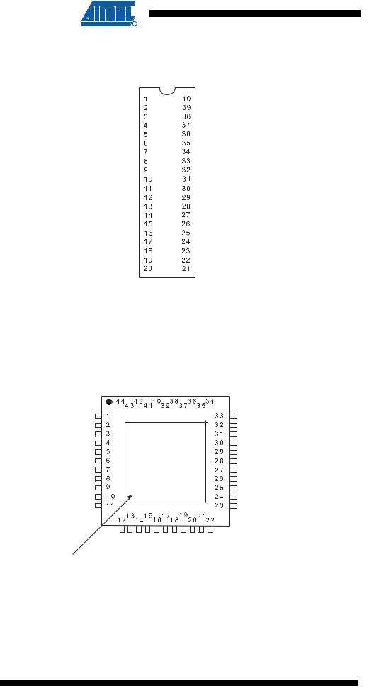
Figure 1. Pinout ATmega16
PDIP
(XCK/T0) PB0 |
|
|
|
PA0 (ADC0) |
||||
|
|
|||||||
|
|
|
||||||
(T1) PB1 |
|
|
|
PA1 (ADC1) |
||||
|
|
|||||||
|
|
|
||||||
(INT2/AIN0) PB2 |
|
|
|
PA2 (ADC2) |
||||
|
|
|||||||
|
|
|
||||||
(OC0/AIN1) PB3 |
|
|
|
PA3 (ADC3) |
||||
|
|
|||||||
|
|
|
||||||
|
(SS) |
PB4 |
|
|
|
PA4 (ADC4) |
||
|
|
|||||||
|
|
|
||||||
(MOSI) PB5 |
|
|
|
PA5 (ADC5) |
||||
|
|
|||||||
|
|
|
||||||
(MISO) PB6 |
|
|
|
PA6 (ADC6) |
||||
|
|
|||||||
|
|
|
||||||
(SCK) PB7 |
|
|
|
PA7 (ADC7) |
||||
|
|
|||||||
|
|
|
||||||
|
|
RESET |
|
|
|
|
AREF |
|
|
|
|||||||
|
|
|
||||||
|
|
|
VCC |
|
|
|
GND |
|
|
|
|||||||
|
|
|
||||||
|
|
|
GND |
|
|
|
AVCC |
|
|
|
|
||||||
|
|
XTAL2 |
|
|
|
PC7 (TOSC2) |
||
|
|
|
||||||
|
|
XTAL1 |
|
|
|
PC6 (TOSC1) |
||
|
|
|
||||||
(RXD) PD0 |
|
|
|
PC5 (TDI) |
||||
|
|
|
||||||
(TXD) PD1 |
|
|
|
PC4 (TDO) |
||||
|
|
|
||||||
(INT0) PD2 |
|
|
|
PC3 (TMS) |
||||
|
|
|
||||||
(INT1) PD3 |
|
|
|
PC2 (TCK) |
||||
|
|
|
||||||
(OC1B) PD4 |
|
|
|
PC1 (SDA) |
||||
|
|
|
||||||
(OC1A) PD5 |
|
|
|
PC0 (SCL) |
||||
|
|
|
||||||
(ICP1) PD6 |
|
|
|
PD7 (OC2) |
||||
|
|
|
||||||
|
|
|
||||||
(MOSI) PB5 (MISO) PB6 (SCK) PB7 RESET VCC GND XTAL2 XTAL1
(RXD) PD0 (TXD) PD1 (INT0) PD2
NOTE:
Bottom pad should
be soldered to ground.
TQFP/QFN/MLF
|
(SS) |
(AIN1/OC0) |
(AIN0/INT2) |
(T1) |
(XCK/T0) |
GND |
|
|
(ADC0) |
(ADC1) |
(ADC2) |
(ADC3) |
||||||||||
|
|
|
||||||||||||||||||||
|
|
|
||||||||||||||||||||
PB4 |
PB3 |
PB2 |
PB1 |
PB0 |
VCC PA0 |
PA1 |
PA2 |
PA3 |
||||||||||||||
|
|
|
|
|
|
|
|
|
|
|
|
|
|
|
|
|
|
|
|
|
|
|
|
|
|
|
|
|
|
|
|
|
|
|
|
|
|
|
|
|
|
|
|
|
|
PA4 (ADC4)
PA5 (ADC5)
PA6 (ADC6)
PA7 (ADC7)
AREF
GND
AVCC
PC7 (TOSC2)
PC6 (TOSC1)
PC5 (TDI)
PC4 (TDO)
PD3 |
PD4 |
PD5 |
PD6 |
PD7 |
VCC GND |
PC0 |
PC1 |
PC2 |
PC3 |
(INT1) |
(OC1B) |
(OC1A) |
(ICP1) |
(OC2) |
|
(SCL) |
(SDA) |
(TCK) |
(TMS) |
Disclaimer
Typical values contained in this datasheet are based on simulations and characterization of other AVR microcontrollers manufactured on the same process technology. Min and Max values will be available after the device is characterized.
2 ATmega16(L)
2466P–AVR–08/07