

Features
•High Performance, Low Power AVR® 8-Bit Microcontroller
•Advanced RISC Architecture
–120 Powerful Instructions – Most Single Clock Cycle Execution
–32 x 8 General Purpose Working Registers
–Fully Static Operation
•Non-volatile Program and Data Memories
–2/4/8K Byte of In-System Programmable Program Memory Flash (ATtiny24/44/84) Endurance: 10,000 Write/Erase Cycles
–128/256/512 Bytes In-System Programmable EEPROM (ATtiny24/44/84) Endurance: 100,000 Write/Erase Cycles
–128/256/512 Bytes Internal SRAM (ATtiny24/44/84)
–Programming Lock for Self-Programming Flash Program and EEPROM Data Security
•Peripheral Features
–Two Timer/Counters, 8- and 16-bit counters with two PWM Channels on both
–10-bit ADC
8 single-ended channels
12 differential ADC channel pairs with programmable gain (1x, 20x) Temperature Measurement
–Programmable Watchdog Timer with Separate On-chip Oscillator
–On-chip Analog Comparator
–Universal Serial Interface
•Special Microcontroller Features
–debugWIRE On-chip Debug System
–In-System Programmable via SPI Port
–External and Internal Interrupt Sources
–Pin Change Interrupt on 12 pins
–Low Power Idle, ADC Noise Reduction, Standby and Power-down Modes
–Enhanced Power-on Reset Circuit
–Programmable Brown-out Detection Circuit
–Internal Calibrated Oscillator
–On-chip Temperature Sensor
•I/O and Packages
–14-pin SOIC, PDIP and 20-pin QFN/MLF: Twelve Programmable I/O Lines
•Operating Voltage:
–1.8 - 5.5V for ATtiny24V/44V/84V
–2.7 - 5.5V for ATtiny24/44/84
•Speed Grade
–ATtiny24V/44V/84V: 0 - 4 MHz @ 1.8 - 5.5V, 0 - 10 MHz @ 2.7 - 5.5V
–ATtiny24/44/84: 0 - 10 MHz @ 2.7 - 5.5V, 0 - 20 MHz @ 4.5 - 5.5V
•Industrial Temperature Range
•Low Power Consumption
–Active Mode:
1MHz, 1.8V: 380 µA
–Power-down Mode:
1.8V: 100 nA
8-bit
Microcontroller with 2/4/8K Bytes In-System Programmable Flash
ATtiny24/44/84
Preliminary
Rev. 8006E–AVR–09/06
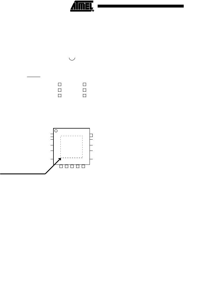
1. Pin Configurations
Figure 1-1. Pinout ATtiny24/44/84
PDIP/SOIC
VCC |
|
1 |
14 |
|
GND |
|
|
||||
(PCINT8/XTAL1) PB0 |
|
2 |
13 |
|
PA0 (ADC0/AREF/PCINT0) |
|
|
||||
(PCINT9/XTAL2) PB1 |
|
3 |
12 |
|
PA1 (ADC1/AIN0/PCINT1) |
|
|
||||
(PCINT11/RESET/dW) PB3 |
|
4 |
11 |
|
PA2 (ADC2/AIN1/PCINT2) |
|
|
||||
(PCINT10/INT0/OC0A/CKOUT) PB2 |
|
5 |
10 |
|
PA3 (ADC3/T0/PCINT3) |
(PCINT7/ICP/OC0B/ADC7) PA7 |
|
6 |
9 |
|
PA4 (ADC4/USCK/SCL/T1/PCINT4) |
(PCINT6/OC1A/SDA/MOSI/ADC6) PA6 |
|
7 |
8 |
|
PA5 (ADC5/DO/MISO/OC1B/PCINT5) |
|
|
|
|
|
|
QFN/MLF
PA5 |
DNC |
|
DNC |
DNC |
PA6 |
|||
|
|
|
|
|
|
|
|
|
|
|
|
|
|
|
|
|
|
Pin 16: PA6 (PCINT6/OC1A/SDA/MOSI/ADC6)
Pin 20: PA5 (ADC5/DO/MISO/OC1B/PCINT5)
(ADC4/USCK/SCL/T1/PCINT4) PA4 
 1 (ADC3/T0/PCINT3) PA3
 2 (ADC2/AIN1/PCINT2) PA2
  3 (ADC1/AIN0/PCINT1) PA1
 4 (ADC0/AREF/PCINT0) PA0
 5
5
NOTE
Bottom pad should be soldered to ground. DNC: Do Not Connect
20 |
19 |
18 |
17 |
6 |
7 |
8 |
9 |
DNC |
DNC |
GND |
VCC |
16
DNC 10
15
14 
13 

12 
11 

PA7 (PCINT7/ICP/OC0B/ADC7) PB2 (PCINT10/INT0/OC0A/CKOUT) PB3 (PCINT11/RESET/dW)
PB1 (PCINT9/XTAL2)
PB0 (PCINT8/XTAL1)
1.1Disclaimer
Typical values contained in this data sheet are based on simulations and characterization of other AVR microcontrollers manufactured on the same process technology. Min and Max values will be available after the device is characterized.
2 ATtiny24/44/84 
8006E–AVR–09/06