

BUS THREE-STATED
BG ASSERTED
BR VALID INTERNAL
BR SAMPLED
BR ASSERTED
CLK
BUS RELEASED FROM THREE STATE AND PROCESSOR STARTS NEXT BUS CYCLE BR NEGATED INTERNAL
BR SAMPLED
BR NEGATED
S0 |
S2 |
S4 |
S6 |
S0 |
S2 |
S4 |
S6 |
S0 |
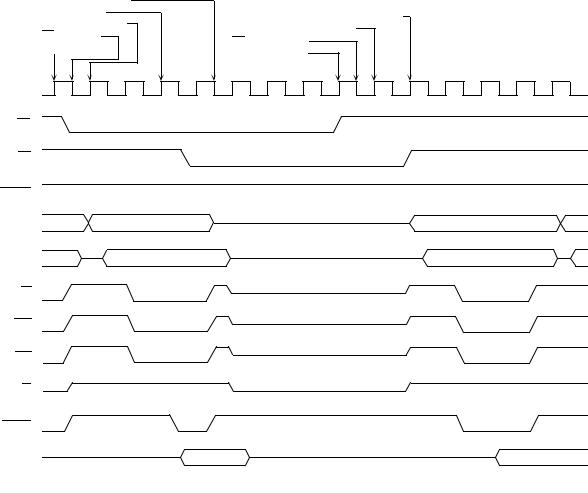
BR
BG
BGACK
FC2–FC0
A23–A1
AS
UDS
LDS
R/W
DTACK
D15–D0
 PROCESSOR
 ALTERNATE BUS MASTER
 PROCESSOR
Figure 5-24. 2-Wire Bus Arbitration Timing Diagram—Special Case
5.4. BUS ERROR AND HALT OPERATION
In a bus architecture that requires a handshake from an external device, such as the asynchronous bus used in the M68000 Family, the handshake may not always occur. A bus error input is provided to terminate a bus cycle in error when the expected signal is not asserted. Different systems and different devices within the same system require different maximum-response times. External circuitry can be provided to assert the bus error signal after the appropriate delay following the assertion of address strobe.
In a virtual memory system, the bus error signal can be used to indicate either a page fault or a bus timeout. An external memory management unit asserts bus error when the page that contains the required data is not resident in memory. The processor suspends execution of the current instruction while the page is loaded into memory. The MC68010 pushes enough information on the stack to be able to resume execution of the instruction following return from the bus error exception handler.
MOTOROLA |
M68000 8-/16-/32-BIT MICROPROCESSORS USER'S MANUAL |
5-23 |

The MC68010 also differs from the other microprocessors described in this manual regarding bus errors. The MC68010 can detect a late bus error signal asserted within one clock cycle after the assertion of data transfer acknowledge. When receiving a bus error signal, the processor can either initiate a bus error exception sequence or try running the cycle again.
5.4.1 Bus Error Operation
In all the microprocessors described in this manual, a bus error is recognized when
DTACK and HALT are negated and BERR is asserted. In the MC68010, a late bus error is also recognized when HALT is negated, and DTACK and BERR are asserted within one clock cycle.
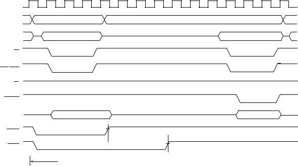
When the bus error condition is recognized, the current bus cycle is terminated in S9 for a read cycle, a write cycle, or the read portion of a read-modify-write cycle. For the write portion of a read-modify-write cycle, the current bus cycle is terminated in S21. As long as
BERR remains asserted, the data and address buses are in the high-impedance state. Figure 5-25 shows the timing for the normal bus error, and Figure 5-26 shows the timing for the MC68010 late bus error.
S0 |
S2 |
S4 |
w |
w |
w |
w |
S6 |
S8 |
CLK
FC2–FC0
A23–A1
AS
LDS/UDS
R/W
DTACK
D15–D0
BERR
HALT
INITIATE |
|
RESPONSE |
|
|
|
BUS ERROR |
|
|
|
INITIATE BUS |
|||
|
READ |
|
|
FAILURE |
|
|
|
DETECTION |
|
|
|
|
|
|
|
|
|
|
|
|
|
ERROR STACKING |
|||||
|
|
|
|
|
|
|
|
|
|||||
Figure 5-25. Bus Error Timing Diagram
5-24 |
M68000 8-/16-/32-BIT MICROPROCESSORS USER'S MANUAL |
MOTOROLA |
S0 |
S2 |
S4 |
S6 |
CLK
FC2–FC0
A23–A1
AS
UDS/LDS
R/W
DTACK
D15–D0
BERR
HALT
|
|
|
|
|
BUS ERROR |
|
|
|
|
INITIATE BUS |
READ CYCLE |
|
|
|
|
|
|
|
|
||
|
|
|
|
DETECTION |
|
|
|
|
ERROR STACKING |
|
|
|
|
|
|
|
|
|
|
||
|
|
|
|
|
|
|
|
|
||
|
|
|
|
|
|
|
|
|
|
|
Figure 5-26. Delayed Bus Error Timing Diagram (MC68010)
After the aborted bus cycle is terminated and BERR is negated, the processor enters exception processing for the bus error exception. During the exception processing sequence, the following information is placed on the supervisor stack:
1.Status register
2.Program counter (two words, which may be up to five words past the instruction being executed)
3.Error information
The first two items are identical to the information stacked by any other exception. The error information differs for the MC68010. The MC68000, MC68HC000, MC68HC001, MC68EC000, and MC68008 stack bus error information to help determine and to correct the error. The MC68010 stacks the frame format and the vector offset followed by 22 words of internal register information. The return from exception (RTE) instruction restores the internal register information so that the MC68010 can continue execution of the instruction after the error handler routine completes.
After the processor has placed the required information on the stack, the bus error exception vector is read from vector table entry 2 (offset $08) and placed in the program counter. The processor resumes execution at the address in the vector, which is the first instruction in the bus error handler routine.
MOTOROLA |
M68000 8-/16-/32-BIT MICROPROCESSORS USER'S MANUAL |
5-25 |
NOTE
In the MC68010, if a read-modify-write operation terminates in a bus error, the processor reruns the entire read-modify-write operation when the RTE instruction at the end of the bus error handler returns control to the instruction in error. The processor reruns the entire operation whether the error occurred during the read or write portion.
5.4.2 Retrying The Bus Cycle
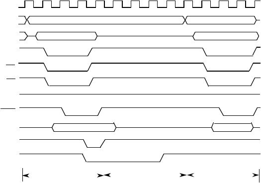
The assertion of the bus error signal during a bus cycle in which HALT is also asserted by an external device initiates a retry operation. Figure 5-27 is a timing diagram of the retry operation. The delayed BERR signal in the MC68010 also initiates a retry operation when
HALT is asserted by an external device. Figure 5-28 shows the timing of the delayed operation.
S0 |
S2 |
S4 |
S6 |
S8 |
S0 |
S2 |
S4 |
S6 |
CLK
FC2-FC0
A23–A1
AS
LDS/UDS
R/W
DTACK
D15–D0
BERR
 ³ 1 CLOCK PERIOD
HALT
READ 
 HALT
HALT 
 RETRY
RETRY 

Figure 5-27. Retry Bus Cycle Timing Diagram
5-26 |
M68000 8-/16-/32-BIT MICROPROCESSORS USER'S MANUAL |
MOTOROLA |
S0 |
S2 |
S4 |
S6 |
S0 |
S2 |
S4 |
S6 |
CLK
FC2–FC0
A23–A1
AS
UDS
LDS
R/W
DTACK
D0–D15
BERR
HALT
READ |
|
HALT |
|
RETRY |
Figure 5-28. Delayed Retry Bus Cycle Timing Diagram
The processor terminates the bus cycle, then puts the address and data lines in the highimpedance state. The processor remains in this state until HALT is negated. Then the processor retries the preceding cycle using the same function codes, address, and data (for a write operation). BERR should be negated at least one clock cycle before HALT is negated.
NOTE
To guarantee that the entire read-modify-write cycle runs correctly and that the write portion of the operation is performed without negating the address strobe, the processor does not retry a read-modify-write cycle. When a bus error occurs during a read-modify-write operation, a bus error operation is performed whether or not HALT is asserted.
5.4.3 Halt Operation (
HALT performs a halt/run/single-step operation similar to the halt operation of an MC68000. When HALT is asserted by an external device, the processor halts and remains halted as long as the signal remains asserted, as shown in Figure 5-29.
MOTOROLA |
M68000 8-/16-/32-BIT MICROPROCESSORS USER'S MANUAL |
5-27 |