

The Microcontroller Idea Book (Jan Axelson, 1994)
.pdfClocks and Calendars
Listing 10-3 (page 1 of 4). Clock and alarm routines for DS1286 Watchdog Timer.
10 |
REM set WT to match address of DS1286 watchdog timer |
||
20 |
WT=0A000H |
|
|
30 |
DO |
|
|
40 |
|
|
|
50 |
PRINT “Select function:” |
|
|
60 |
PRINT “Initialize and start clock 1" |
||
70 |
PRINT “Display time and day |
2" |
|
80 |
PRINT “Set alarm |
3" |
|
90 |
INPUT A |
|
|
100 |
IF A=1 THEN |
GOSUB 200 |
|
110 |
IF A=2 THEN |
GOSUB 1000 |
|
120 |
IF A=3 THEN |
GOSUB 2000 |
|
130 |
WHILE 1=1 |
|
|
140 |
END |
|
|
200 |
REM initialize and start clock |
|
|
210 |
REM stop clock while initializing |
|
|
220 |
XBY(WT+9)=XBY(WT+9).OR.80H |
|
|
230REM get time and date, convert each value to BCD and store
240 |
INPUT “year (0-99)? ”,X |
|
250 |
GOSUB 3000 |
|
260 |
XBY(WT+0AH)=X |
|
270 |
INPUT “month (1-12)? ”,X |
|
280 |
GOSUB 3000 |
|
290 |
XBY(WT+9)=(XBY(WT+9).AND.0E0H)+X |
|
300 |
INPUT “day of month (1-31)? ”,X |
|
310 |
GOSUB 3000 |
|
320 |
XBY(WT+8)=X |
|
330 |
INPUT “day of week (1-7)? ”,X |
|
340 |
GOSUB 3000 |
|
350 |
XBY(WT+6)=X |
|
360 |
INPUT “24-hr (0) or 12-hr (1) clock? ”,TT |
|
370 |
IF TT=0 THEN GOSUB 3000 ELSE |
GOSUB 600 |
380 |
INPUT “minutes (0-59)? ”,X |
|
390 |
GOSUB 3000 |
|
400 |
XBY(WT+2)=X |
|
410 |
INPUT “seconds (0-59)? ”,X |
|
420 |
GOSUB 3000 |
|
430 |
XBY(WT+1)=X |
|
440 |
XBY(WT)=0 |
|
The Microcontroller Idea Book |
181 |
|

Chapter 10
Listing 10-3 (page 2 of 4).
450 PRINT “Press any key when ready to start the clock” 460 A=GET : IF A=0 THEN GOTO 460
470 XBY(WT+9)=(XBY(WT+9)).AND.7FH
480 RETURN
500 |
INPUT “hour (0-23)? ”,X |
510 |
GOSUB 3000 |
520 |
XBY(WT+4)=X |
530 |
RETURN |
590 |
REM set up 12-hour clock |
600 |
INPUT “hour (1-12)? ”,X |
610 |
INPUT “AM (0) or PM (1)? ”,AP |
620 |
GOSUB 3000 |
630 |
XBY(WT+4)=X+AP*20H+TT*40H |
640 |
RETURN |
1000 |
REM display current time and date |
1010 |
REM clear TE for error-free reads |
1020 |
XBY(WT+0BH)=XBY(WT+0BH).OR.80H |
1030 |
REM get hours |
1040 |
X=XBY(WT+4).AND.1FH |
1050 |
GOSUB 3100 |
1060 |
PRINT “Time = ”,X,":", |
1070 |
REM get minutes |
1080 |
X=XBY(WT+2) |
1090 |
GOSUB 3100 |
1100 |
PRINT X,":", |
1110 |
REM get seconds |
1120 |
X=XBY(WT+1) |
1130 |
GOSUB 3100 |
1140 |
PRINT X, |
1150 |
IF TT=0 THEN 1220 |
1160 |
IF AP=1 THEN 1190 |
1170 |
PRINT “am” |
1180 |
GOTO 1220 |
1190 |
PRINT “pm” |
1200 |
182 |
The Microcontroller Idea Book |

Clocks and Calendars
Listing 10-3 (page 3 of 4).
1210 REM get month
1220 X=XBY(WT+9).AND.3FH
1230 GOSUB 3100
1240 PRINT “Date = ”,X,"/",
1250 REM get day of month
1260 X=XBY(WT+8)
1270 GOSUB 3100
1280 PRINT X,"/",
1290 REM get year
1300 X=XBY(WT+0AH)
1310 GOSUB 3100
1320 PRINT X
1330 REM get day of week
1340 X=XBY(WT+6)
1350 GOSUB 3100
1360 PRINT “Day of week = ”,X
1370 REM set TE when reads are done
1380 XBY(WT+0BH)=XBY(WT+0BH.OR.80H)
1390 RETURN
2000 REM set alarm
2010 PRINT “Select alarm type:”
2020 PRINT “Once per minute (1)”
2030 PRINT “When minutes match (2)”
2040 PRINT “When hours and minutes match (3)”
2050 PRINT “When hours, minutes, and days match (4)”
2060 INPUT AF
2070 REM clear all 3 alarm mask bits
2080 XBY(WT+3)=XBY(WT+3).AND.7FH
2090 XBY(WT+5)=XBY(WT+5).AND.7FH
2100 XBY(WT+7)=XBY(WT+7).AND.7FH
2110 REM set alarm mask bits as needed
2120 IF AF<4 THEN XBY(WT+7)=XBY(WT+7).OR.80H
2130 IF AF<3 THEN XBY(WT+5)=XBY(WT+5).OR.80H
2140 IF AF=1 THEN XBY(WT+3)=XBY(WT+3).OR.80H
2150 IF AF>1 THEN INPUT “Minute? ”,M
2160 IF AF>2 THEN INPUT “Hour? ”,H
2170 IF AF=4 THEN INPUT “Day? ”,D
The Microcontroller Idea Book |
183 |

Chapter 10
Listing 10-3 (page 4 of 4).
2180 REM store alarm settings
2190 IF AF1 THEN X=M : GOSUB 3000 : XBY(WT+3)=80H+X 2200 IF AF2 THEN X=H : GOSUB 3000 : XBY(WT+5)=80H+X 2210 IF AF=4 THEN X=D : GOSUB 3000 : XBY(WT+7)=80H+X 2220 REM turn on alarm
2230 REM time-of-day alarm is edge-triggered, low-going, INTA 2240 XBY(WT+0BH)=0D8H
2250 DO
2260 ONEX1 3200
2270 WHILE 1=1
2280 RETURN
3000 |
REM convert decimal to BCD |
3010 |
X=INT(X/10)*16+X-INT(X/10)*10 |
3020 |
RETURN |
3100 |
REM convert BCD to decimal |
3110 |
X=INT(X/16)*10+(X/16-INT(X/16))*16 |
3120 |
RETURN |
3200 |
REM alarm interrupt routine |
3210 |
PRINT “ALARM” |
3220 |
GOSUB 1000 |
3230 |
RETI |
184 |
The Microcontroller Idea Book |

Control Circuits
11
Control Circuits
This chapter presents a variety of ways to use an 8052-BASIC system for computer control. The applications include switching power to a load, controlling a matrix of switches, selecting the gain of an op amp, and controlling speed and direction of stepping and dc motors.
Switching Power to a Load
You can use your 8052-BASIC system’s port bits to control power to all kinds of devices, including those powered by alternating current (AC), or direct current (DC) at voltages other than 5 volts. Figure 11-1 shows two port bits that control solid-state relays that switch power to AC and DC loads.
A solid-state relay is a simple, safe way to switch power to devices that require high voltages or currents. A logic voltage at the relay’s control inputs determines whether or not power is applied to the load.
In a typical solid-state relay, the control voltage is electrically isolated from the switching circuits, which contain an optoisolated triac or a similar device. Many AC solid-state relays include zero-switching circuits, which reduce noise by switching power only when the AC signal is near zero volts.
The Microcontroller Idea Book |
185 |

Chapter 11
Figure 11-1. Solid-state relays provide an easy way to switch power to AC or DC loads..
Using a solid-state relay saves you the trouble of building a similar circuit from discrete components. Surplus relays are inexpensive, as low as $1.50 each, from vendors such as All Electronics, Marlin Jones, and Hosfelt. If you don’t have a data sheet for your relay, look for a pair of control pins, usually labeled + and -. The other two pins connect to the load.
In Figure 11-1, the control bits are outputs of a 74LS374 latch addressed at E400h, as described in Chapter 6. On a normally open relay, the load switches on when its control bit is low. If you want a logic high to turn on the load, wire an inverter between the ’374’s output and the relay, or use a normally closed relay. Or you can use a 74HCT374 latch in place of
186 |
The Microcontroller Idea Book |

Control Circuits
the LSTTL part, and wire the desired bit to the relay’s + input, with the relay’s - input connected to GND.
Look for a relay with a control voltage of 5 volts or less, and input control current of 15 milliamperes or less. The relay’s rated output voltages and currents should be greater than those of the load you intend to switch.
Take care to work safely when you’re wiring, testing, and using circuits that control high-current or high-voltage loads. For circuits that connect to 117V line voltage and have a metal chassis, you can ground the chassis by connecting it to the safety-ground wire in a 3-wire power cord. Insulate any exposed wires and terminals with heat-shrinkable tubing. If in doubt about how to wire the power connections, get qualified help before you continue.
You can control a relay from any output port bit. Just write a 1 or 0 to the corresponding bit to switch the load on or off. If you control a solid-state relay with a port bit on an 8255 or the 8052-BASIC, you may have to add an LSTTL or HCMOS buffer (such as a 74LS244) to supply enough current to the relay’s control inputs.
Controlling a Switch Matrix
Figure 11-2 shows how you can use 9 output bits to control an 8 x 8 array of electronic switches. You can connect any of eight X inputs to any of eight Y inputs, in any combination. Possible applications include switching audio or video signals to different monitors or recording instruments, selecting inputs for test equipment, or any situation that requires flexible, changeable routing of analog or digital signals.
A Mitel MT8808 8 x 8 analog switch array simplifies the circuit design and programming. The chip contains an array of crosspoint switches, plus a decoder that translates a 6-bit address into a switch selection, and latches that control the opening and closing of the switches. Maxim is another source for switch arrays like this.
Connecting an X and Y input requires the following steps: Write the X and Y addresses to AX0-AX2 and AY0-AY2. Bring STB high. Bring DATA high to close the switch. Bring STB low to latch the data. To open a connection between an X and Y input, you do the same but bring DATA low to open the switch.
You can make and break as many connections as you want by writing the appropriate values to the chip. All previous switch settings remain until you change them by writing to the specific switch.
You can connect the switches in any combination. For example, you can connect one X input to each of the eight Y inputs, to create eight distinct signal paths. Or, you can connect all eight Y inputs to a single X input, to route one signal along eight different paths.
The Microcontroller Idea Book |
187 |

Chapter 11
The MT8808 is shown powered at +5V, but VDD may be anywhere from 4.5V to 13.2V. VEE is an optional negative supply that enables you to switch negative signals.
The switches do have some resistance, which varies with the supply voltage. At 5V, typical switch resistance is 120 ohms; at 12V, it drops to 45 ohms. This should cause no problems in switching standard LSTTL or CMOS signals. If you are routing an analog voltage to a low-impedance input, the switch resistance may attenuate the signal. Maximum switching frequency of the chip is 20 Megahertz.
In Figure 11-2, the switch array is controlled by Port A and bit 7 of Port C (PC.7) on an 82C55 PPI. Bringing PC.7 high opens all of the switches. If you don’t need this ability, you can tie RESET low and use PC.7 for something else.
You can use any output port bits to control the MT8808. Logic high inputs at the MT8808 must be at least 3.5V, though, so if you use NMOS or TTL outputs, add a 10K pull-up resistor from each output to +5V.
For a simple test of the switches, you can connect a series of equal resistors as shown to the X inputs. Each X input will then be at a different voltage. To verify a switch closure, measure the voltages at the selected X and Y inputs; they should match.
Figure 11-2. With the MT8808 switch array, an 8-bit output port can connect eight X inputs to eight Y inputs, in any combination.
188 |
The Microcontroller Idea Book |

Control Circuits
Listing 11-1. Controls an MT8808 switch matrix.
10 |
REM A=base address of 82C55 |
20 |
A=0FC00H |
30 |
REM configure 8255 for all outputs |
40 |
XBY(A+3)=80H |
50 |
REM bring MT8808’s Reset low (off) |
60 |
XBY(A+3)=0EH |
70 |
XBY(A)=0 |
80 |
DO |
90 |
INPUT “Open (0), close (1), or reset all (2)? ”,Z |
100 |
IF Z=2 THEN GOSUB 300 |
110 |
IF Z THEN GOSUB 400 |
120 |
WHILE 1=1 |
130 |
END |
290 |
REM reset all switches by toggling Reset |
300 |
XBY(A+3)=0FH |
310 |
XBY(A+3)=0EH |
320 |
RETURN |
400 |
PRINT “Enter inputs to connect or open: ” |
410 |
INPUT “X (0-7)? ”,X |
420 |
INPUT “Y (0-7)? ”,Y |
430 |
REM write to MT8808 to open or close selected switch |
440 |
B=X+Y*8+Z*40H |
450 |
XBY(A)=B |
460 |
XBY(A)=B+80H |
470 |
XBY(A)=B |
480 |
RETURN |
Listing 11-1 demonstrates switch operation by asking you whether to open or close a switch or reset them all, then performing the requested action.
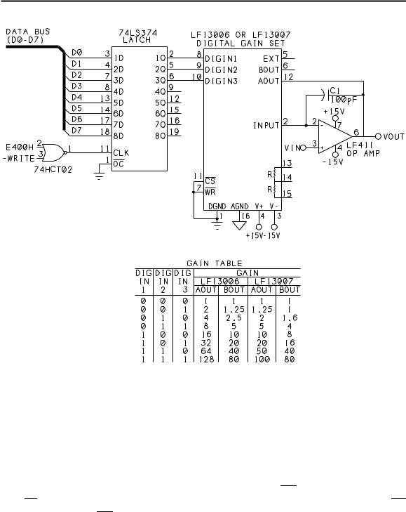
Op Amp with Programmable Gain
Figure 11-3 shows a way to set the gain of an operational amplifier by writing to three output port bits. Controlling the gain is National Semiconductor’s LF13006 or LF13007 digital- gain-set IC. Each contains a resistor ladder, switches, and decoding logic that enable you to select any of eight gains for an amplifier, attenuator, current source, or other circuit that requires precise, variable outputs.
Each of the gain-set ICs has two outputs, each with a different series of gains, as Figure 11-3 shows. The gain error is guaranteed to be 0.5 percent or less over the full range of operating temperatures.
The Microcontroller Idea Book |
189 |
Chapter 11
Figure 11-3. An LF13006/7 controls the gain of an LF411 op amp.
The bits that select the gain are outputs of a 74LS374 latch addressed at E400h. The LF13006/7’s Chip-Select and Write pins are tied low, which causes the gains at pins 12 and 6 to immediately match the settings at DIGIN1-DIGIN3.
If you want to control up to four gain-set chips and op amps, you can use the five remaining outputs of the 74LS374 to select the desired chip. Tie all of the WR inputs to one bit, and tie each CS input to one of the remaining bits. Then, to set the gain of an op amp, bring its CS input low, then bring WR low, then high to latch the data to the desired chip.
You can use just about any op amp with this circuit. Shown is an LF411, which has a wide bandwidth and low input offset and drift. A 10-picofarad capacitor from the op amp’s input
190 |
The Microcontroller Idea Book |