

A T M E L A P P L I C A T I O N S
Number 1 • Summer, 2003
Special AVR
Microcontrollers
ISSUE
In issue:
•Atmel Notes
•Novice’s Guide to AVR Development
•Basic Interrupts and I/O
•Device Drivers and the Special Function Register Hell
•Variable Message Sign Development
•GPS-GSM Mobile Navigator
•AT86RF401 Reference Design
•Designer’s Corner
•Atmel AVR and Third-Party Tools Support
•And More.
 R
R

Our AVR microcontroller is probably 12 times faster than the one you’re using now.
(It’s also smarter.)
Introducing the Atmel AVR®. An 8-bit MCU that can help you beat the pants off your competition.
AVR is a RISC CPU running single cycle instructions. With its rich, CISC-like instruction set and 32 working registers,
it has very high code density and searingly fast execution–up to 16 MIPS. That’s 12 times faster than conventional 8-bit micros. We like to think of it as 16-bit performance at an 8-bit price.
With up to 128 Kbytes of programmable Flash and EEPROM, AVR is not only up to 12 times faster than the MCU you’re using now. It’s probably 12 times smarter, too.
And when you consider that it can help slash months off your development schedule and save thousands of dollars in project cost, it could make you look pretty smart, too.
AVR comes in a wide range of package and performance options covering a huge number of consumer and industrial applications. And it’s supported by some of the best development tools in the business.
So get your project started right. Check out AVR today at www.atmel.com/ad/fastavr. Then register to qualify for your free evaluation kit and bumper sticker. And get ready to take on the world.
CheckoutAVRtodayatwww.atmel.com/ad/fastavr
AVR 8-bit RISC Microcontrollers |
Memory Configurations (Bytes) |
Debug and |
|
|
|
|
|
|||
Processor |
Package |
Flash |
EEPROM |
RAM |
Development Tools |
|
|
|
|
|
tinyAVR |
8-32pin1-2K |
upto128 |
upto128 |
|
Available |
|
|
|
||
™ |
|
|
|
|
|
|
|
|
|
|
lowpowerAVR |
81--44pin8K upto512 |
upto1K |
|
Available |
|
|
R |
|||
|
|
|
||||||||
megaAVR® 32-64pin8-128K upto4K |
upto4K |
|
Available |
|
|
|||||
|
|
|
|
|
|
|
|
|
|
|
©2002AtmelCorporation.AtmelandtheAtmellogoareregisteredtrademarksofAtmelCorporation.

A T M E L A P P L I C A T I O N S J O U R N A L
Welcome to the AVR Edition of the Atmel Applications Journal
Jim Panfil,
Director of Marketing
By Jim Panfil, Director of Marketing
The AVR Microcontroller introduced by Atmel in 1997 is the only new 8- bit Architecture launched in the last two decades. During the first six years of production, the AVR attracted twenty thousand new customers because of its unique in-system programmable Flash program memory and price performance.
The success of the AVR Architecture is due in part to the large and growing number of partners and suppliers offering products and services that reduce development and programming time and cost. Developers using the AVR in their next application require all manner of support including design services; help in using new tools, compilers and the ability to communicate and share lessons learned with other engineers who encountered and solved similar problems. In addition to the application notes on the Atmel web site and AVR Freaks.com users forum, we now have our own publication-- the Atmel Applications Journal. Here is the charter issue, dedicated to the AVR Microcontroller.
|
|
AVR Family Roadmap |
1997 |
2000 |
2003 |
|
|
ASIC AVR |
|
|
TINY AVR |
|
TINY AVR |
RF AVR |
|
|
|
|
|
AVR |
|
AVR |
USB AVR |
AVR |
|
|
|
SECURE AVR |
|
|
MEGA AVR |
|
|
|
|
|
|
MEGA AVR |
|
FPGA AVR |
LCD AVR |
|
|
|
|
|
CAN AVR |
|
|
FPGA AVR |
|
|
DVD AVR |
The Mega AVR Family has a unique Self-Programming Memory and Read while Write capability. This is a break through technology that enables new applications and provides the user a significant cost reduction by eliminating additional circuitry including a second CPU to implement remote programming capability. Today the AVR is more than a solution supporting the general-pur- pose marketplace. The product family now integrates unique peripheral functions that provide solutions for specialized markets. Examples are the portable appliances, wireless communication, security and PC segments.
Atmel recently introduced four new application specific extensions to the AVR Family. The Mega 169 is the first member of a family of devices with an inte-
4-WIRE IN/OUT |
|
3-WIRE IN/OUT |
|
|
|
JTAG |
|
SERIAL |
|
|
|
FLASH |
PERIPHERAL |
|
|
EEPROM |
|
INTERFACE |
|
|
|||
|
|
INTERFACE |
|
|
|
|
|
|
|
|
ANALOG |
|
|
|
|
|
COMPARATOR |
OCD |
|
PROGRAM |
|
|
|
|
|
|
A/D |
||
|
|
COUNTER |
|
||
|
|
|
|
|
CONVERTER |
|
|
|
|
|
LCD |
INSTRUCTION |
|
|
|
INTERFACE |
|
|
|
|
|
||
|
REGISTER |
32 GENERAL |
|
|
|
|
|
|
|
||
|
|
PURPOSE |
|
|
|
|
|
RIGISTERS |
|
USART |
|
CONTROL |
|
|
|
|
|
|
|
|
|
|
|
LINES |
|
|
|
|
|
|
|
|
|
|
SPI |
INSTRUCTION |
RAM |
|
|
|
|
ALU |
|
|
|
||
REGISTER |
|
|
|
|
|
|
|
|
|
CPU |
TWI |
|
|
|
|
|
|
WATCHDOG |
I/O |
INTERRUPTS |
|
TIMER/ |
|
TIMER |
PORTS |
COUNTERS |
|
||
|
|
||||
AVR Chip Diagram
AVR Roadmap
grated LCD controller. Typical power consumption is less than 20uA at 32KHz operation. It targets battery-powered applications like residential thermostats, portable medical instruments and cordless communication devices.
The AT86RF401 SmartRF processor combines the AVR with a high performance RF transmitter operating at 250 – 460MHz.
It is targeted at cost sensitive wireless remote control markets such as auto keyless entry, garage door openers and home convenience controls. The AT97SC3201 Trusted Computing Platform Module brings affordable hardware security to the PC Platform. It consists of an AVR with sophisticated tamper detection circuitry designed to be mounted on the motherboard of the smallest platforms including pocket PC’s and PDA’s. AT90SC Secure AVR Family integrates a random word generator, crypto coprocessor and on chip security to enable GSM SIM card, Internet transaction, pay TV and banking designs. These smart card applications require high performance to perform encryption functions in real time. There are six members of the USB AVR product offering. The AT43USB351M is the only configurable low / high speed USB controller supporting five end points. With integrated 12 channel 10-bit A/D capability, it supports video game controllers, data acquisition devices, and sensors and mass storage applications.
Based on unprecedented market acceptance and customer demand, Atmel created two new AVR design teams. One is located in Nantes, France, the other in Helsinki, Finland. These teams have specialized DSP, analog and communication protocol design skills, which will expand the product portfolio and open new markets for the AVR. To ensure adequate production capacity, we commissioned a new 8-inch wafer Fab in Tyneside, UK. This facility is capable of processing twelve thousand eight-inch wafers per week with geometries as small as 0.13u technology. This new production facility will accelerate cost reduction efforts for both existing and new AVR components. Atmel has made a significant investment in design capability, process technology, plant and equipment to ensure that state of the art AVR solutions are readily available and are cost effective.
www.atmel.com
page 1

A T M E L A P P L I C A T I O N S Number 1 • Summer, 2003
T A B L E O F C O N T E N T S
1
Welcome to the AVR Edition of the Atmel Applications Journal
By Jim Panfil, Atmel
5
An Inexpensive Altitude Deviation Alert
By Larry Rachman, Innovation Design and Solutions, Inc.
6
Novice’s Guide to AVR Development
By Eivind A. Sivertsen, Sean Ellis & Arild Rødland, AVR Freaks
11
Basic interrupts and I/O
By Eivind A. Sivertsen, Sean Ellis & Arild Rødland, AVR Freaks
18
Device Drivers and the Special Function Register Hell
By Evert Johansson, IAR Systems
4-WIRE IN/OUT |
3-WIRE IN/OUT |
|
|
page 1 |
|
|
|
FLASH |
INTERFACE |
|
EEPROM |
|
|
|
|
|
|
|
ANALOG |
|
|
|
COMPARATOR |
|
PROGRAM |
A/D |
|
|
COUNTER |
|
|
|
|
|
CONVERTER |
|
|
|
LCD |
|
|
|
INTERFACE |
|
32 GENERAL |
|
|
|
PURPOSE |
|
|
|
RIGISTERS |
USART |
|
|
|
|
|
|
|
|
SPI |
|
RAM |
|
|
|
ALU |
|
|
|
|
CPU |
TWI |
|
|
|
|
I/O |
INTERRUPTS |
TIMER/ |
|
PORTS |
COUNTERS |
|
|
page 28
19
Variable Message Sign Development with AVR and ImageCraft
By Patrick Fletcher-Jones and Chris Willrick
20
GPS-GSM Mobile Navigator
By Ma Chao & Lin Ming
25
AT86RF401 Reference Design
By Jim Goings, Atmel
page 11 28
An RF-Controlled Irrigation System
By Brian Miller
32
Departments
Atmel Notes |
Page 3 |
Designer’s Corner |
Page 32 |
Atmel AVR Third Party Tools |
Page 34 |
Atmel AVR Devices |
Page 35 |
Atmel AVR Tools & Software |
Page 37 |
www.atmel.com
page 2
 R
R

A T M E L A P P L I C A T I O N S J O U R N A L
Atmel Notes...
First secureAVR Microcontroller with 32Mega-bit Flash
Atmel® Corporation announced that it is sampling a secureAVR™ RISC Microcontroller with 32Mega-bit Flash. This product is based on the AT90SC3232CS (secureAVR processor, 32Kbytes Flash, 32Kbytes EEPROM) with in addition 32Mega-bit of Flash for very efficient and secure data storage. The AT90SC3232CS-F32M is a unique and innovative solution that combines programmability and processing power with a very large Flash memory.
With the AT90SS3232CS-F32M, mobile communication operators have access to a powerful product for emerging applications with an important secure memory in a SIM card. For other applications, wherever any system requires a large amount of data to be protected, the AT90SC3232CSF32M provides a highly secure, high memory capacity solution.
The AT90SC3232CS-F32M offers all of the AT90SC3232CS features, a flexible secure microcontroller using Flash program memory to satisfy a user's code modification requirements. For example, its state-of-the-art security features that make it resistant against the most aggressive hardware or software attacks and its powerful cryptography capabilities (Elliptic Curves hardware support, fast DES/TDES and fast RSA processor). It is designed to meet Common Criteria EAL4+ security certification. The AT90SC3232CS-F32M is available in a 3V version, as well as 5V, and can be delivered in module form or in package form.
Herve Roche, Smart Card IC Marketing Manager stated, "The content protection barrier is being surpassed. The AT90SC3232CS-F32M is the industry's first high-end secure microcontroller with this type of large Flash memory capacity. The other great performance is the availability of this outstanding product for the smart card market with deliveries in
module form. For example the ITSO's (Interoperable Transport Smartcard Organization) secure access module has been developed with the AT903232CS-F32M in a standard SIM format". The AT90SC3232CSF32M is available in engineering samples. The price for
1000 units is $20.
IAR visualSTATE® for AVR tool entry updated
Automated design and code generation with IAR visualSTATE for AVR:
The first state machine graphical design tool generating highly compact C code for embedded systems
•Automatic generation of C/C++ code from state machine models
•Automatic generation of full documentation
•Intuitive, easy to use graphical editor
•Full verification and simulation tools including on-target debug capability using RealLink
•UML compliant state machine standard
IAR visualSTATE allows you to represent your specification/requirement in a graphical state machine model, debug, simulate, document and generate micro-tight C code for your embedded device.
Benefits include:
•Faster development through graphical design of any application
•Rapid implementation of change requests avoiding C code rewrite
•Accurate, structured documentation that is always in-sync with the final design
•Interactively simulate and model your system before committing to hardware
•Embedded applications that are much easier to maintain
•Generate micro-tight embedded C code from graphical design with a single mouse click
A Fully Integrated USB Secure µC Solution in a Single Package
Atmel Corporation is sampling a fully integrated USB FullSpeed secure microcontroller in a PQFP44 package. The AT90SC6464C-USB-I integrated package solution that requires no external clock is based on Atmel's secureAVR(TM) RISC microcontroller. It includes 128Kbytes of on-chip non-volatile memory, powerful cryptography capabilities, a very high level of physical and data security, and a dual interface USB V2.0 Full-Speed interface as well as the standard ISO 7816 smart card interface.
The AT90SC6464C-USB-I targets eTokens used in PC-based secure applications. This package solution can also be embedded in peripherals, set-top boxes, modems, PDAs (Personal Digital Assistants), copyright protection devices and other equipment. Wherever data needs to be protected, the AT90SC6464C-USB-I can provide highly secure and costeffective solutions in applications such as transactional security, e-mail and network encryption, software and file protection, MP3 and digital camera data storage protection.
The AT90SC6464C-USB-I features a dual communication interface, including both USB V2.0 Full-Speed (12 Mbps)
and ISO 7816, for direct connection to either of these popular communication parts. It also incorporates 64Kbytes of on-chip Flash memory and 64Kbytes of EEPROM. Flash program memory gives unrivalled flexibility for new applications with the ability to load or upgrade application code during the production run with no delay.
The AT90SC6464C-USB-I includes all the security features already built into the AT90SC secure microcontroller series. In particular, it provides a 16-bit RISC crypto processor for very efficient execution of the highest-level encryption algorithms, RSA, AES 128/128, SHA-256. In addition, a hardware T-DES (Triple Data Encryption Standard) coprocessor, a true RNG (Random Number Generator) and support for ECC (Elliptic Curve Cryptography) enhance the high cryptography performance of this device.
The AT90SC6464C-USB-I in PQFP44 package is available now in engineering samples. Production quantities are also available at a price of US $4.00 in quantities of 200.000 units.
www.atmel.com
page 3

A T M E L A P P L I C A T I O N S J O U R N A L
Atmel Notes... continued
Atmel Extends the 8-bit AVR Product Family
New Devices Serve Wireless,
PC Peripheral and Security Markets
Atmel announced today four new application specific extensions to the AVR Family. The AVR Microcontroller introduced by Atmel in 1997 is the industry's only new 8-bit Architecture launched in the last two decades. During the first six years of production, the AVR has become the design engineers' microcontoller of choice because of its unique insystemprogrammable Flash program memory and price performance. Today the AVR represents more than a solution supporting the general-purpose marketplace as the product family now integrates unique peripheral functions that provide solutions for specialized markets. Examples of this integration now support wireless communication, security and PC peripheral segments.
The four new application specific extensions to the AVR Family include the AT86RF401 SmartRF processor, which combines the AVR with a high performance RF transmitter operating at 250 - 460MHz. It is targeted at cost sensitive wireless remote control markets such as auto keyless entry, garage door openers and home convenience controls.
The second application specific area is covered by the AT90SC Family Secure AVR, which integrates a random word generator, crypto coprocessor and on chip security to enable GSM SIM card, Internet transaction, pay TV and banking designs. These smart card applications require high performance to perform encryption functions in real time. There are six members of the USB AVR product offering. The AT43USB351M is the only configurable low / high speed
USB controller supporting five end points. With integrated 12 channel 10-bit A/D capability, it supports video game controllers, data acquisition devices, and sensors and mass
storage applications.
Finally, the Mega 169 is the first member of a family of devices with integrated LCD con- t r o l l e r .
Ty p i c a l p o w e r
consumption is less than 20uA at 32KHz operation. It targets battery-powered applications like residential thermostats, portable medical instruments and LCD cordless communication devices.
"Based on unprecedented market acceptance and customer demand Atmel created two new AVR design teams located in Nantes, France and Helsinki, Finland in addition to those in San Jose, CA, Rousset, France and Trondheim, Norway to work on further expanding this award winning product portfolio. These teams have specialized skills in analog, DSP and communication protocol design which will open new markets for the AVR." Said Jim Panfil, Director of Microcontroller Products. To ensure adequate production capacity, we commissioned a new 8-inch wafer Fab in Tyneside, UK. This facility is capable of processing ten thousand eight-inch wafers per week with geometries as small as 0.13u technology. We are making a significant investment in design capability, process technology, plant and equipment to accelerate the growth of the AVR portfolio." He added.
PDAs and other electronic equipment. The ability to authenticate OEM subassemblies within a system, including removable storage devices, automotive piece parts, and replaceable components such as printer cartridges, is now an affordable option.
"We are pleased with the technology advancements we have made in our secure portfolio over the last few months. We are well positioned to provide leading edge solutions to the security and embedded markets," said Kerry Maletsky, Business Unit Director for Atmel Corporation. "This new technology secures Atmel's position as the only semiconductor manufacturer to provide an affordable, secure solution for embedded applications."
High volume pricing of these new products in package form range from $.30 to $.85 depending on memory density.
Atmel Announces a New Secure Memory Solution for Embedded Applications
Boasting the industry's ONLY family of secure memory devices with data encryption
Atmel announced that its CryptoMemory® product line is now available in plastic packages. These integrated circuits are the industry's only low cost, high security memory chips with data encryption utilizing synchronous protocols for embedded applications. The CryptoMemory family of products, available from 1K bit to 256K bits, fills an industry need for affordable, secure devices for customers who require traditional plastic packages. CryptoMemory's secure nonvolatile EEPROM provides the customer with data security through an authentication protocol, data encryption and tamper protection circuits. A common 2-wire serial interface is used for fast data rate exchanges. This innovative technology, which previously was available in physical forms suitable for only the smart card market, opens up new opportunities for customers who need embedded security at an affordable price.
The CryptoMemory family can be used to secure an endless array of embedded applications, including authenticating individual users who need access to sensitive information and securing data on printed circuit boards, networking systems,
Publisher: Glenn ImObersteg
glenn@convergencepromotions.com
Managing Editor: Bob Henderson
bob@convergencepromotions.com
Designer: Dave Ramos
dbyd@garlic.com
This Special Issue of the Atmel Applications Journal is published by Convergence Promotions. No portion of this publication may be reproduced in part or in whole without express permission, in writing, from the publisher. Copyright © Atmel corporation 2003. Atmel®, AVR® and combinations thereof, and megaAVR®, tinyAVR® are the registered trademarks, and AVRStudio™ and SecurAVR™ are the trademarks of Atmel Corporation or its subsidiaries. AVRFreaks®, IAR Systems, Innovative Design and Solutions, Inc®, Visual State®, eTokens®, Motorola®, and ARM® are the trademarks of their respective companies. All product copyrights and trademarks are property of their respective owners. All other product names, specifications, prices and other information are subject to change without notice. The publisher takes no responsibility for false or misleading information or omissions. Any comments may be addressed to the publisher, Convergence Promotions at 2220 Sunset Point, Discovery Bay, CA 94514.
Printed in the USA.
www.atmel.com
page 4

A T M E L A P P L I C A T I O N S J O U R N A L
Overview
A complex and expensive regulatory approval process for avionics equipment in the US and other countries has created a market for accessories and devices that, since not connected directly to the aircraft, are exempt from the approval process. Such devices are expected to be substantially less expensive than panelmounted equipment,
yet the pilot-user's expectation of low cost is still accompanied by one for high reliability, ease of operation, and the small size expected of a portable device. Our challenge was to provide an altitude deviation alarm that
would alert the pilot to an inadvertent climb or descent, possibly into restricted airspace. Given recent global events, such deviations are subject to quick and often extreme
www.atmel.com
An Inexpensive Altitude Deviation Alert
By Larry Rachman, Innovation Design and Solutions, Inc.
Background
Altitude is most commonly measured by its non-linear relationship to air pressure (Figure 1). At sea level, air pressure is approximately 30 in. Hg (100 kPa), decreasing to approximately 13 in. Hg (45 kPa) at an altitude of 18,000 feet (5500 m). Traditionally altimetry is performed by mechanical means – a sealed air bellows is subject to atmospheric pressure; its dimensional changes are geared to move indicators on a mechanical display, or to operate a Gray-coded encoder wheel providing the information in electronic form. Cost and size limitations would not permit such a solution for this project; instead a monolithic piezoresistive pressure sensor was used. The device is comprised of a sealed vessel con-
taining a known air pressure, one wall of which is a silicon die incorporating a micromachined strain gauge and amplification stage. The package design permits air pressure to be introduced to the other side of the die, causing it to deflect due to the pressure differential. A buffered voltage proportional to the pressure differential is provided as output.
Figure 1
Our goal was to sound an alert upon a deviation as small as 100-200 feet. This required a resolution of 4 millivolts over a range of 2.3 volts, corresponding to an Analog-to-Digital Converter resolution of 10 bits, before allowing for granularity, hysteresis, or low-order-bit ADC noise. Ideally, a resolution of 1314 bits would be needed to accomplish our goal.
Design Strategy
Our processor selection was the Atmel AVR at90s4433, chosen for size, cost, and low power consumption. The part includes an excellent low-power ADC, but with a resolution of only 10 bits. There are numerous serial ADC devices available in the market, but costs tend to rise above 10-12 bits. With cost, size, and power consumption all factors, we decided to re-examine our design requirements. In normal operation the voltage corresponding to the altitude
Air |
|
|
|
Pressure |
Gain |
AVR |
Audio |
Transducer |
and |
at90s4433 |
|
|
offset |
to Intercom |
|
|
microcontroller |
||
|
stage |
|
|
|
|
Resistor |
|
|
|
Ladder |
|
|
|
DAC |
|
Figure 2
being measured is static, though it may be static at any point over a range of 2.3 to 4.6 volts. If the voltage were scaled to the point where the required 4 millivolt resolution were measurable with the AVR ADC, it would be out of range for other altitudes.
The problem was solved by implementing a 4-bit resistor ladder Digital to Analog Converter driven by the AVR controller. The output of this DAC was used to control the offset of the gain stage between the pressure sensor and the ADC. (Figure 2) This permitted a step selection to be made by the AVR firmware, insuring that the voltage being measured was within the ADC rails. Since only a delta measurement was being made, the DAC could be constructed with relatively low-precision resistors (1%). By choosing offset and gain stage values appropriately, the steps were overlapped, permitting any voltage over the input range to be offset to a point in the center 80% of the ADC range.
When a stable altitude is reached a button press initiates a search for the DAC output step that will cause the ADC input to fall near the center of its range. Based on the step selected, the firmware can compensate for the non-lineari- ty of the relationship between altitude and air pressure. The deviation alert is generated both by LED indicator and an audio tone introduced into the aircraft intercom system. The tone is generated with one of the AVR programmable timers, with a second timer used for both system timing and control of the tone cadence. Different tones indicating climb, descent, return to proper altitude, and low battery (detected by another ADC channel) are generated while the processor spends approximately 99% of its time asleep, saving power.
The application firmware was developed using Atmel AVR Studio, the ICE200, and the Imagecraft AVR Compiler. The AVR's complier-friendliness allowed the application to be implemented in C with code size being only a minor factor. Source-level debugging simplified the development effort and later bug fixes. During debugging, software state and ADC input values were reported to the AVR serial port, simplifying the development process.
A 0.050" (1.27 mm) PCB card-edge pattern was included in the PCB design for the AVR in-system programming connections. The connector also included power and ground connections, permitting one-step production programming of the AVR in-situ, without bed-of-nails ICT fixturing, and with zero additional component cost.
Conclusion
By re-examining our design goals, we were able to utilize the ADC in the at90s4433, where at first this did not seem possible. With the exception of a buffer, the AVR was the only digital part in our design, keeping both cost and size to a minimum. (PCB dimension was 2x2" (50x50 mm) including connectors and the pressure transducer) With a remaining code space of 50%, as well as a pin-compatible growth path in the Mega8, we have an ample growth path for new features.
FOOTNOTES:
1- Several drawings of a conventional barometric altimeter have been made available at http://www.4innovation.biz/altimeter
2- Motorola MPX5100 series, http://www.motorola.com/webapp/sps/site/ prod_summary.jsp?code=MPX5100&nodeId=01126990368716
3- Imagecraft, http://www.imagecraft.com/software/ adevtools.html
page 5

A T M E L A P P L I C A T I O N S J O U R N A L
An Introduction intended for people with no prior AVR knowledge..
By Arild Rødland,
AVRFreaks
Starting with a new µC architecture can be quite fustrating. The most difficult task seems to be how to get the information and documentation to get the first AVR program up running.
This tutorial assumes that you do not yet own any AVR devices or AVR development tools. It also assumes that you have no prior knowledge of the AVR architecture or instruction set. All you need to complete this tutorial is a computer running some flavour of the Windows operating system, and an internet connection to download documents and files.
Novice’s Guide to AVR Development
Preparing your PC for AVR Development
Let's make an easy start, and download the files that we will need later on. First you should download the files to have them readily available when you need them. This could take some time depending on your internet connection.
Download these files to a temporary folder on your computer. ( e.g. C:\Temp ):
|
|
|
|
|
|
|
|
AVR STUDIO 4 |
|
This file contains the AVR Studio 4 Program. This |
|
||
|
(~15MB) |
|
program is a complete development suite, and |
|
||
|
|
|
contains an editor and a simulator that we will |
|
||
|
|
|
use to write our code, and then see how it will |
|
||
|
|
|
run on an AVR device. |
|
||
|
Assembly Sample Code |
|
|
|
|
|
|
|
|
|
|
|
|
|
|
This file contains the Assembly Sample code |
|
|||
|
(~1kB) |
|
you will need to complete this guide. |
|
|
|
|
AT90S8515 Datasheet |
|
|
|
|
|
|
|
|
|
|
|
|
|
|
This is the Datasheet for the AT90S8515 AVR |
|
|||
|
(~4MB) |
|
Microcontroller. This is a convenient "Getting |
|
|
|
|
|
|
Started" device. For now you don't have to worry |
|
|
|
|
|
|
about the different types of AVR micros. You'll see |
|
|
|
|
|
|
that they are very much alike, and if you learn |
|
|
|
|
|
|
how to use one (eg. 8515), you will be able to |
|
|
|
|
|
|
use any other AVR without any problems. |
|
|
|
|
Instruction Set Manual |
|
|
|
|
|
|
|
|
|
|
||
|
|
This is the Instruction Set Manual. This document |
|
|||
|
(~2MB) |
|
is very useful if you want detailed information |
|
|
|
|
|
|
about a specific instruction. |
|
|
|
|
|
|
|
|
|
|
|
|
|
|
|
|
|
|
|
|
|
|
|
|
When you have downloaded the files, it is time to install the software you need.
Step 2. Installing AVR Studio 4
AVR Studio is also available in a version 3. We will use AVR Studio 4 since this is the version that will eventually replace version 3.
Important note for people using Windows NT/2000/XP:
You must be logged in with administrator rights to be able to successfully install AVR Studio. The reason is that these Windows systems have restrictions regarding who can install new device drivers!
Installation:
1)Double click on the AVRSTUDIO.EXE file you downloaded. This file is a self extracting file, and will ask where you want to extract the files. The default path points to your "default" temp folder, and could be quite well "hidden" on your hard disk, so make sure to read and remember this path, or enter a new path to where you want the files placed (e.g. c:\temp )
2)Once all the files are extracted, open the temp folder, and double click on the SETUP.EXE file. Just follow the installation, and use the default install path. NB: You can use another path, but this tutorial assumes that you install it to the default path.
That's it. Now you have installed all the software you'll need to write code and run programs for all available AVR devices! Keep the Datasheet and Instruction set Manual in a place you remember.
Basic AVR Knowledge
The AVR Microcontroller family is a modern architecture, with all the bells and whistles associated with such. When you get the hang of the basic concepts the fun of exploring all these features begins. For now we will stick with the "Bare Bone" AVR basics.
The 3 different Flavors of AVR
The AVR microcontrollers are divided into three groups:
•tinyAVR
•AVR (Classic AVR)
•megaAVR
The difference between these devices lies in the available features. The tinyAVR µC are usually devices with lower pin-count or reduced feature set compared to the megaAVR's . All AVR devices have the same instruction set and memory organization, so migrating from one device to another AVR is easy.
Some AVR's contain SRAM, EEPROM, External SRAM interface, Analog to Digital Converters, Hardware Multiplier, UART, USART and the list goes on.
If you take a tinyAVR and a megaAVR and strip off all the peripheral modules mentioned above, you will be left with the AVR Core. This Core is the same for all AVR devices. (Think of Hamburgers: They all contain the same slab of meat, the difference is the additional styling in the form of tripled-cheese and pickles :)
Selecting the "correct" AVR
The morale is that the tinyAVR, AVR (Classic AVR) and megaAVR does not really reflect performance, but is more an indication of the "complexity" of the device: Lot's of features = megaAVR, reduced feature set = tinyAVR . The "AVR (Classic AVR)" is somewhere in between these, and the distinctions between these groups are becoming more and more vague.
So for your project you should select an AVR that only includes the features that you need if you are on a strict budget. If you run your own budget you should of course go for the biggest AVR possible, since eh... because!
Learning to write code on the AVR
Learning new stuff is fun, but can be a bit frustrating. Although it is fully possible to learn the AVR by only reading the datasheet this is a complicated and timeconsuming approach. We will take the quick and easy approach, which is:
1.Find some pre-written, working code
2.Understand how this code works
3.Modify it to suite our needs
The device we will use is the AT90S8515 which is an AVR with a good blend of peripherals. Take a few minutes to browse through the Datasheet.
Learning to use the AVR Datasheets
It is easy to get scared when looking at the AVR Datasheets. E.g. the ATmega128(L) datasheet is almost 350 pages long, and reading it start to finish - and remembering the contents, is quite a task. Luckily you are not supposed to do that, either. The datasheets are complete technical documents that you should use as a reference when you are in doubt how a given peripheral or feature works.
www.atmel.com
page 6

A T M E L A P P L I C A T I O N S J O U R N A L
OK! You have now installed the software, you have a vague knowledge of the different types of AVRs, and know that there is a lot of information in the datasheet that you don't yet know anything about! Good, now it's time to get developing! Click "Next"
to advance to the next part of this tutorial.
When you open an AVR Datasheet you will discover that it can be divided into these groups:
1.First Page Containing Key information and Feature List
2.Architectural Overview
3.Peripheral Descriptions
4.Memory Programming
5.Characteristics
6.Register Summary
7.Instruction Set Summary
8.Packaging Information
This is quite convenient. When you are familiar with how to use the AT90S8515 Datasheet, migrating to another Datasheet should be a breeze. After completing this tutorial you should take some time and read through the Architectural Overview sections of the datasheets (At the beginning of the Datasheets). These sections contain a lot of useful information about AVR memories, Addressing modes and other useful information.
Another useful page to look at is the Instruction Set Summary. This is a nice reference when you start developing code on your own. If you want in-depth information about an instruction, simply look it up in the Instruction Set Manual you previously downloaded!
OK! You have now installed the software, you have a vague knowledge of the different types of AVRs, and know that there is a lot of information in the datasheet that you don't yet know anything about! Good, now it's time to get developing! Click "Next" to advance to the next part of this tutorial.
AVR Studio 4 GUI
Note: If you have not yet installed AVR Studio you should go to the Preparing your PC for AVR Development section of this tutorial before continuing.
Step 1: Creating a New Project
Start AVR Studio 4 by launching AVR Studio 4 located at [START] | [Programs] | [Atmel AVR Tools]. AVR Studio will start up, and you will get this dialog box.
We want to create a new Project so press the "Create New Project Button"
Step 2: Configuring Project Settings
This step involves setting up what kind of project we want to create, and setting up filenames and location where they should be stored.
This is done in four steps:
1.Click on this to let the program know you want to create an Assembly program
2.This is the name of the project. It could be anything, but "Leds" is quite descriptive of what this program is going to do
3.Here you can specify if AVR Studio should automatically create a initial assembly file. We want to do this. The filename could be anything, but use "Leds" to be compatible with this tutorial!
4.Select the path where you want your files stored
5.Verify everything once more, and make sure both check-boxes are checked. When you are satisfied, press the "Next >>" button
Step 3: Selecting Debug Platform
The AVR Studio 4 Software can be used as a frontend software for a wide range of debugging tools.
1. AVR Studio 4 supports a wide range of emulation and debugging tools. Since we have not purchased any of these yet, we will use the built in simulator functionality.
2. ..and we want to develop for the AT90S8515 device
3.Verify all settings once more, then press "Finish" to create project and go to the assembly file
Step 4: Writing your very first line of code
AVR Studio will start and open an empty file named Leds.asm. We will take a closer look at the AVR Studio GUI in the next lesson. For now note that the Leds.asm is not listed in the "Assembler" folder in the left column. This is because the file is not saved yet. Write in this line: "; My Very First AVR Project" as shown in the figure below. The semicolon ; indicates that the rest of the line should be treated as a comment by the assembler.
To save the line press - S or select [Save] on the [File] menu. The Leds.asm will now show up in the Left Column as shown below.
www.atmel.com
page 7

A T M E L A P P L I C A T I O N S J O U R N A L
At this point you should have installed
the software, and started up the a new project called "Leds" You should also have the AT90S8515 Datasheet, stored somewhere you can easily find it. If you can answer "Yes" to both these questions, you are ready to continue writing some AVR Code.
OK, Now that we have AVR Studio up and running, it's time to take a closer look at the AVR Studio GUI..
AVR Studio 4 GUI
Let's take a closer look at the AVR Studio Graphical User Interface (GUI).
As you can see below, we have divided the GUI into 6 sections. AVR Studio 4 contains a help system for AVR Studio, so instead of reinventing the wheel here, I'll just explain the overall structure of AVR Studio 4 and point to where in the AVR Studio 4 On-line Help System you can find in depth information.
1.The first line here is the "Menus" Here you will find standard windows menus like save and load file, Cut & Paste, and other Studio specific menus like Emulation options and stuff.
2.The next lines are Toolbars, which are "shortcuts" to commonly used functions. These functions can be saving files, opening new views, setting breakpoints and such.
3.The Workspace contains Information about files in your Project, IO view, and Info about the selected AVR
4.This is the Editor window. Here you write your assembly code. It is also possible to integrate a C-Compiler with AVR Studio, but this is a topic for the more advanced user
5.Output Window. Status information is displayed here.
6.The System Tray displays information about which mode AVR Studio is running in. Since we are using AT90S8515 in simulator mode, this will be displayed here
More about the GUI
To complete this bare bone guide you don't need any more knowledge of the GUI right now, but it is a good idea to take a look at the AVR Studio HTML help system. You can start this by opening [HELP] [AVR Studio User Guide] from AVR Studio, or by clicking this link (and select: Open) if you installed AVR Studio to the default directory. When you have had your fill, we'll continue working on our first AVR Program.
Writing your First AVR Program
At this point you should have installed the software, and started up the a new project called "Leds" You should also have the AT90S8515 Datasheet, stored somewhere you can easily find it. If you can answer "Yes" to both these questions, you are ready to continue writing some AVR Code.
In the Editor view in AVR Studio, continue your program (which at this point only consists of the first line below) by adding the text top of next colum. (Cheaters can simply cut & paste the source below into AVR Studio...)
|
Sample Code |
(~1kB) |
|
|
;My Very First AVR Project |
|
|
||
.include |
"8515def.inc" |
;Includes the 8515 |
||
|
|
definitions |
file |
|
.def Temp = R16 |
;Gives "Defines" Register |
|||
|
|
R16 the name Temp |
||
.org 0x0000 |
;Places the |
following code |
||
|
|
from address 0x0000 |
||
rjmp |
RESET |
;Take a Relative Jump to the |
||
|
|
RESET |
Label |
|
RESET: |
|
;Reset |
Label |
|
ldi Temp, 0xFF |
;Store 255 in R16 (Since we |
|||
|
|
have defined R16 = Temp) |
||
out DDRB, Temp |
;Store this value in The |
|||
|
|
PORTB |
Data |
direction |
|
|
Register |
|
|
Loop: |
|
;Loop |
Label |
|
out PORTB, Temp |
;Write all |
highs |
||
|
|
(255 decimal) to PORTB |
||
dec Temp |
;Decrement |
R16 (Temp) |
||
rjmp Loop |
;Take a relative jump to the |
|||
|
|
Loop label |
|
|
Note that the source code changes color when written in the editor window. This is known as syntax highlighting and is very useful make the code more readable. Once the Source code is entered, press CTRL + F7 or select [Build and Run] from the [Project] Menu.
In the output view (at the bottom left of the screen) you should get the following output indicating that the Project compiled correctly without any errors! From this output window, we can also see that our program consists of 6 words of code (12 bytes).
Congratulations!! You have now successfully written your first AVR program, and we will now take a closer look at what it does!
Note: If your program does not compile, check your assembly file for typing errors. If you have placed the include files (8515def.inc) in a different folder than the default, you may have to enter the complete path to the file in the
.include "c:\complete path\8515def.inc" statement. When it compiles we will continue explaining and then debugging the code.
www.atmel.com
page 8
I guess you have figured out what our masterpiece is doing. We have made a counter counting down from 255 to 0, but what happens when we
reach zero?
www.atmel.com
A T M E L A P P L I C A T I O N S J O U R N A L
Understanding the Source Code
OK so the code compiled without errors. That's great, but let us take a moment to see what this program does, and maybe get a feeling how we should simulate the code to verify that it actually performs the way we intended. This is the complete source code:
Sample Code
;My Very First AVR Project
.include "8515def.inc" ;Includes the 8515 definitions file
.def Temp = R16 |
;Gives "Defines" Register R16 |
|
the name Temp |
.org 0x0000 |
;Places the following code |
|
from address 0x0000 |
rjmp RESET |
;Take a Relative Jump to the |
|
RESET Label |
RESET: |
;Reset Label |
ldi Temp, 0xFF |
;Store 255 in R16 (Since we |
|
have defined R16 = Temp) |
out DDRB, Temp |
;Store this value in The |
|
PORTB Data direction Register |
Loop: |
;Loop Label |
out PORTB, Temp |
;Write all highs |
|
(255 decimal) to PORTB |
dec Temp |
;Decrement R16 (Temp) |
rjmp Loop |
;Take a relative jump to the |
|
Loop label |
Now let's take a line-by-line look at what's going on in this code.
;My Very First AVR Project
Lines beginning with " ; " (semicolon) are comments. Comments can be added to any line of code. If comments are written to span multiple lines, each of these lines much begin with a semicolon
.include "8515def.inc"
Different AVR devices have e.g. PORTB placed on different location in IO memory. These .inc files maps MNEMONICS codes to physical addresses. This allows you for example to use the label PORTB instead of remembering the physical location in IO memory (0x18 for AT90S8515)
.def Temp = R16
The .def (Define) allow you to create easy to remember labels (e.g. Temp) instead of using the default register Name (e.g. R16). This is especially useful in projects where you are working with a lot of variables stored in the general purpose Registers (The Datasheet gives a good explanation on the General Purpose Registers!)
.org 0x0000
This is a directive to the assembler that instructs it to place the following code at location 0x0000 in Flash memory. We want to do this so that the following RJMP instruction is placed in location 0 (first location of FLASH). The reason is that this location is the Reset Vector, the location from where the program execution starts after a reset, power-on or Watchdog reset event. There are a also other interrupt vectors here, but our application does not use interrupts, so we can use this space for regular code!
rjmp RESET
Since the previous command was the .org 0x0000, this Relative Jump (RJMP) instruction is placed at location 0 in Flash memory, and is the first instruction to be executed. If you look at the Instruction Set Summary in the Datasheet, you will see that the AT90S8515 do not have a JMP instruction. It only has the RJMP instruction! The reason is that we do not need the full JMP instruction. If you compare the JMP and the RJMP you will see that the JMP instruction has longer range, but requires an additional instruction word, making it slower and bigger. RJMP can reach the entire Flash array of the AT90S8515, so the JMP instruction is not needed, thus not implemented.
RESET:
This is a label. You can place these where you want in the code, and use the different branch instructions to jump to this location. This is quite neat, since the assembler itself will calculate the correct address where the label is.
ldi Temp, 0xFF
Ah.. finally a decent instruction to look at: Load Immediate (LDI). This instruction loads an Immediate value, and writes it to the Register given. Since we have defined the R16 register to be called "Temp", this instruction will write the hex value 0xff (255 decimal) to register R16.
out DDRB, Temp
Why aren't we just writing "ldi DDRB, Temp"? A good question, and one that require that we take a look in the Instruction Set Manual. Look up the "LDI" and "OUT" instructions. You will find that LDI has syntax : "LDI Rd, K" which means that it can only be used with General Purpose Registers R16 to R31. Looking at "OUT" instruction we see that the syntax is "OUT A, Rr" Which means that the content that is going to be written by the OUT instruction has to be fetched from one of the 32 (R0 to R31) General Purpose Registers.
Anyway, this instruction sets the Data Direction Register PORTB (DDRB) register to all high. By setting this register to 0xFF, all IO pins on PORTB are configured as outputs.
Loop
Another label...
out PORTB, Temp
We Now write the value 0xFF to PORTB, which would give us 5V (Vcc) on all PORTB IO pins if we where to measure it on a real device. Since the IO ports is perhaps the most used feature of the AVR it would be a good idea to open the Datasheet on the PORTB. Notice that PORTB has 3 registers PORTB, PINB and DDRB. In the PORTB register we write what we want written to the physical IO pin. In the PINB register we can read the logic level that is currently present on the Physical IO pin, and the DDRB register determines if the IO pin should be configured as input or output. (The reason for 3 registers are the "Read-Modify-Write" issue associated with the common 2 register approach, but this is a topic for the Advanced class.)
dec Temp
This Decrement (DEC) instruction decrements the Temp (R16) register. After this instruction is executed, the contents of Temp is 0xFE. This is an Arithmetic instruction, and the AVR has a wide range of Arithmetic instructions. For a complete listing of available instruction: Look in the Instruction Set Summary in the Datasheet!
rjmp Loop
Here we make a jump back to the Loop lable. The program will thus continue to write the Temp variable to PORTB decrementing it by one for each loop.
I guess you have figured out what our masterpiece is doing. We have made a counter counting down from 255 to 0, but what happens when we reach zero?
Simulating with the Source Code
AVR Studio 4 operates in different "modes". Back when we where writing the code, we where in editor mode, now we are in debugging mode. Lets take a closer look at these:
1.Note that a Yellow arrow has appeared on the first RJMP instruction. This arrow points to the instruction that is about to be executed.
2.Note that the workspace has changed from Project to IO view. The IO view is our peek-hole into the AVR, and it will probably be your most used view. We will look closer at this one in a short while.
3.The bottom line contains status information. This Reads:
AT90S8535 Simulator, Auto, Stopped. This is followed by a yellow icon. It is a good idea to check this information to verify that you have selected the correct device and emulation tool.
page 9

A T M E L A P P L I C A T I O N S J O U R N A L
After running through this introduction you should have a basic idea of how to get a program up and running on the
AVR µC.
Setting up the IO View
Since our program mainly operates on PORTB registers, we will expand the IO view so that we can take a closer look at the contents of these register. Expand the IO view (tree) as shown in the figure on left:
Stepping through the Code
AVR Studio allows running the code at full speed until a given point, and then halt. We will
however take if nice and slow, and manually press a button for every instruction that should be executed. This is called single-stepping the code.
Press [ F11 ] once. This is the key for single-stepping. Note that the yellow arrow is now pointing at the LDI Temp, 0xFF instruction. This is the instruction that is going to be executed next.
Press [ F11 ] once more. The LDI instruction is executed, and the arrow points to the OUT instruction. The Temp Register has now the value 0xFF. (If you open the "Register 16-31" tree you will see that R16 contains 0xFF. We defined Temp to be R16, remember?)
Press [ F11 ]. DDRB is now 0xFF, As shown in the IO View above this is represented as black squares in the IO View. So, a white square represents logical low "0" and black squares are logical high "1". By setting DDRB high, all bits of PORTB is configured as outputs.
Press [ F11 ]. 0xFF is now written to PORTB register, and the arrows points to the DEC instruction. Note that PORTB is equal to 0xFF. Note also that the PINB register is still 0x00!
Press [ F11 ]. The Temp variable is decremented (0xFF - 1 = 0xFE). In addition the PINB register changes from 0x00 to 0xFF! Why? To find out why this happens you have to look at the PORT sections of the datasheet. The explanation is that the PORTB is first latched out onto the pin, then latched back to the PIN register giving you a 1 clock cycle delay. As you can see, the simulator behaves like the actual part! The next instruction is a relative jump back to the Loop label.
Press [ F11 ]. The RJMP is now executed, and the arrow is back pointing at the OUT PORTB, Temp instruction.
Press [ F11 ] to write the new Temp value to the PORTB register. Note that the content of PORTB is now updated to 0xFE! Continue pressing F11 until you have counted down the PORTB register to 0x00. What happens if you continue running the Program?
Conclusion and Recommended Reading
After running through this introduction you should have a basic idea of how to get a program up and running on the AVR µC.
As mentioned before, one of the most efficient methods of learning AVR programming is looking at working code examples, and understanding how these work. Here on AVRfreaks.net you will find a large collection of projects suitable to learn you more about the AVR.
In our tools section we have also linked up all Atmel AVR Application Notes.
These are also very useful reading.
www.atmel.com
page 10

A T M E L A P P L I C A T I O N S J O U R N A L
an introduction to interrupts and I/O with the AVR
Eivind, AVRfreaks.net,
By Eivind Sivertsen,
AVRFreaks
Oct.2002
This article is a small project for you people who are just getting into the AVR, and perhaps even microcontrollers in general.
Basic Interrupts and I/O
Lets' get physical
The natural place to start is the STK500. It is a very nice development board for the AVR, reasonably priced (~USD79) and provides all the environment we need to test some pretty real applications on the AVR out in the wild.
We're gonna start out with some simple counting controlled by external interrupts and exposed on the nice LEDs of the STK500. Then we'll add a speaker (Oh yeah!), and before we know it we'll have a miniature amusement park on our desks; with lights AND noise and buttons to push! Perhaps fire as well, if something REALLY goes wrong.
This is what we'll use:
1.AVRstudio 3 or 4
2.STK500 development kit, all set up with your computer and ready to go
3.An AT90s8515 microcontroller (usually comes with the STK500)
4.Some small speaker that works, including wires soldered in place
The setup is based on a Windows configuration, but it is very possible use some other software as well, since we won't concentrate much on the use of AVRstudio besides assembling the project. If you are a Linux user, you could use:
*avr-gcc (i.e. avrasm) for the assembly
*uisp for programming
The program will be written in assembly, because:
*assembly is very "machine-near" and provides a very educative approach to what goes on inside the processor during our program
*high-level languages and different compilers all have different notations and routines for doing the same thing. Learning a compiler and the respective C-style (e.g.) is a story of itself.
The code for this project is something we found among leftovers from O'Guru Sean Ellis; which we brutally and without due respect ripped apart. Shame on us.
Basic interrupts
An interrupt is a flow control mechanism that is implemented on most controllers, among them the AVR. In an MCU application interacting with the outside world, many things are happening at the same time, i.e. not in a synchronized manner, that are to be handled by the microcontroller.
Examples: a switch pressed by the user, a data read on the UART (serial port), a sample taken by the ADC, or a timer calling to say that "time is up!". All these events neeeds to be handled by the MCU.
Instead of polling each instance round-Robin style to ask whether they are in need of a service, we can have them call out themselves when they need attention. This is called "interrupts", since the peripheral device (e.g. a switch pressed) interrupts the main program execution. The processor then takes time out of the normal program execution to examine the source of the interrupt and take the necessary action. Afterwards, normal program execution is resumed.
An interrupt service in other words is just like a subroutine; except that it is not anticipated by the processor to occur at a particular time, since there are no explicitly placed calls to it in the program.
What's in a name?
When reading this article you will from time to time get the feeling that you are confronting a term possibly denoting an actual physical entity or an entity in some sense relevant to the current activity; namely playing around or building serious applications with the AVR...: INT0, INT1, GIMSK, PORTB, PB7 etc...
You are sure to come across such names in any assembly code, Atmel appnote, AVRfreaks Design Note or any posting in the AVRforum.
One might think these are just common names used by individuals accustomed to the jargon, but we will try to use them consciously - in the sense that these names actually denote actual memory locations in the AVR you will be programming.
The mapping of these name to actual memory locations is in the part's def file (*def cacros vn unknown term:
8515def.inc |
Example snippet; only a few lines are shown |
|||
|
;***** |
I/O Register Definitions |
||
|
.equ |
SREG |
=$3f |
|
|
.equ |
SPH |
=$3e |
|
(~6kB) |
.equ |
SPL |
=$3d |
|
.equ |
GIMSK |
=$3b |
||
|
||||
|
.. |
.. |
.. |
|
|
.. |
.. |
.. |
|
|
|
|
|
|
When including this file in the assembly program file, all I/O register n a m e s and I/O register bit names appearing in the data book will be known to the assembler and can be used in the program.
Note that some high-level language compilers may use proprietary terms other than these. But they will have files similar to this def file, defining the memory space of the AVRs. As previously stated; this is another story.
Another document that will prove very useful to anyone working with the AVR, is this document:Manual you previously downloaded!
8515 datasheet
The datasheet.
(~2MB)
The datasheet is the ultimate reference for any AVR microcontroller. It even includes an instruction set summary; look up every instruction you don't know when you come across it!
www.atmel.com
page 11

A T M E L A P P L I C A T I O N S J O U R N A L
The vector table is reserved for storing interrupt vectors; i.e. locations to jump to when this or that interrupt is calling. This means that each interrupt has a reserved memory location, and when a particular interrupt comes in, the MCU looks in this location to find the address where code that handles this interrupt resides.
In this article, we will be using the 8515. Download this .pdf and keep it close for reference.
You may even want to print it, but think twice.
It is long.
Now you know where to look when anything unknown pops up. Let's move on >.
Structure of an interrupt-driven program on the AVR
Take a deep breath. This is the heaviest part.
We are going to write an "interrupt-driven" program where the main loop simply does nothing but wait for interrupts to occur. What interrupts?
External interrupts INT0 and INT1 on pins PD2 and PD3
The interrupts are handled in turn, and a return to the main program is performed at the end of each interrupt service (that's what I call it; "service"). This is a rather wide topic with many pitfalls. But we need somewhere to start and will mainly discuss aspects concerning elements of our little example application. The main important thing that constitutes such elements in a program is:
1.Setting the interrupt vector jump locations: .org
2.Setting the correct interrupt mask to enable desired interrupts: GIMSK
3.Make necessary settings in control registers: MCUCR
4.Globally enable all interrupts: SREG
Setting the interrupt vector jump locations: .org
The lowest part of the AVR program memory, starting at address $0000, is sometimes referred to as the "Program memory vector table", and the actual program should start beyond this space.
The vector table is reserved for storing interrupt vectors; i.e. locations to jump to when this or that interrupt is calling. This means that each interrupt has a reserved memory location, and when a particular interrupt comes in, the MCU looks in this location to find the address where code that handles this interrupt resides.
8515 Vector table |
|
Example; only the few first |
|
|
vectors are shown |
Program memory address |
Vector |
Comment |
$0000 |
Reset |
Start address of Reset handler is stored here |
$0001 |
INT0 |
Start address of code to handle external INT0 is stored |
|
|
here |
$0002 |
INT1 |
Start address of code to handle external INT1 is stored |
|
|
here |
etc... |
... |
... |
The number of interrupts available varies from processor to processor.
The .org directive
In assembly code, the .org directive is used to set vector jump locations. This assembler directive (or "command", if you like) tells the assembler to set the location counter to an absolute value. It is not part of the AVR instruction set, it is just a command that the assembler needs to make sure the program code is mapped correctly when making a binary for the AVR.
Example:
Sample Code
;Interrupt service vectors
;Handles reset and external interrupt vectors INT0 and INT1
.org $0000 |
|
rjmp Reset |
; Reset vector (when the MCU is reset) |
.org INT0addr |
|
rjmp IntV0 |
; INT0 vector (ext. interrupt from |
|
pin PD2) |
.org INT1addr |
|
rjmp IntV1 |
; INT1 vector (ext. interrupt from |
|
pin PD3) |
; - Reset vector - (THIS LINE IS A COMMENT) Reset:
ldi
out
ldi
out
...
...
Note that labels are used instead of absolute numbers to designate addresses in assembly code - The assembler stitches it all together in the end. All we need to do is tell the assembler where to jump when e.g. the reset vector is calling, by using the name of the code block meant for handling resets.
A label denotes a block of code, or function if you like; which is not terminated with a "}", an .endfunc or anything like that. The only thing that ends a code block definition, is it being released by another block name, followed by a colon (":").
This also implies, unlike with functions in e.g. C, that all blocks are run by the processor consecutively, unless the flow is broken up by un/conditional jumps, returns, interrupts etc. In assembly, the whole file is the main( ) function, and the flow control is more like Basic...
Please also note the first lines of the reset handler. This is where the stack is set up. The stack is used to hold return addresses in the main program code when a subor interrupt routine is run; i.e. when a "digression" from the main program is made. For any interrupt service or subroutine to return to the main program properly; the stack must be placed outside their vector space. The SP is namely initialized with the value $0000, which is the same location as the reset vector. This goes for any program, especially such as this, where we are involving several interrupt vectors besides the reset vector.
For AVRs with more than 256 bytes SRAM (i.e. none of the Tinys, nor 2343 and 4433), the Stack Pointer register is two bytes wide and divided into SPL and SPH (low and high bytes).
Setting the interrupt mask: GIMSK
The GIMSK register is used to enable and disable individual external interrupts.
GIMSK |
|
General Interrupt Mask register |
||||||
Bit |
7 |
6 |
5 |
4 |
3 |
2 |
1 |
0 |
|
INT1 |
INT0 |
- |
- |
- |
- |
- |
- |
Read/write |
R/W |
R/W |
R |
R |
R |
R |
R |
R |
Init. value |
0 |
0 |
0 |
0 |
0 |
0 |
0 |
0 |
Note that only the INT0 and INT1 bits are writable. The other bits are reserved and always read as zero.
www.atmel.com
page 12
A T M E L A P P L I C A T I O N S J O U R N A L
This is what our code will do. Nothing more. Besides initialization, the short routine for
handling the other switch (generating INT1) and a few directives for the assembler, that's it all.
We are going to use the external interrupts INT0 and INT1 for the switches on the STK500. These interrupts are enabled by setting INT0 and INT1 in GIMSK; i.e. bits 6 and 7.
MCUCR |
|
|
|
MCU general control register |
||||
Bit |
7 |
6 |
5 |
4 |
3 |
2 |
1 |
0 |
|
ISRE |
SRW |
SE |
SM |
ISC11 |
ISC10 ISC01 |
ISC00 |
|
Init. value |
0 |
0 |
0 |
0 |
0 |
0 |
0 |
0 |
The bits in MCUCR allow general processor control.
Consult the datasheet for an in-depth description of the registers and the individual bits.
We will be using bits 0,1,2 and 3 in this register to control the interrupt from INT0 and INT1. These bits control how to sense the external interrupts; either by level, falling edge on pin, or rising edge of pin:
ISCx1 |
ISCx0 |
Description |
0 |
0 |
Low level on INTx pin generates interrupt |
0 |
1 |
Reserved |
1 |
0 |
Falling edge on INTx pin generates interrupt |
1 |
1 |
Rising edge on INTx pin generates interrupt |
|
|
|
We will use the rising edge of the switches on the STK500 to trig the interrupt; so the 8515 must be programmed to trig external interrupts on rising edges of each pin PD2 and PD3. Hence; all the ISCx bits must, for our program, be set to "1".
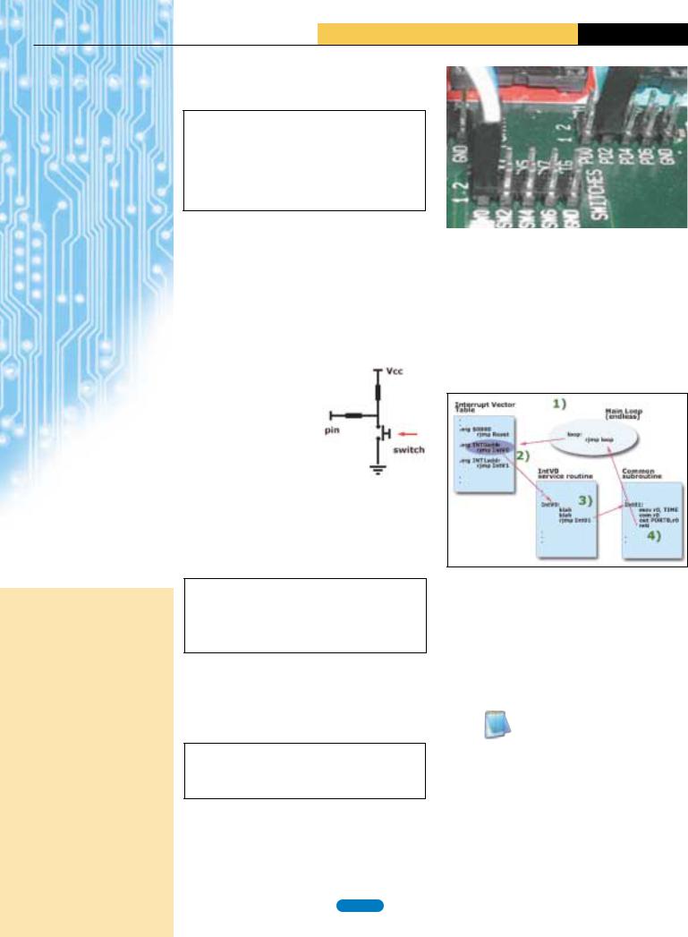
You can see on the diagram to the right how pushing the switch will close the lower
branch and pull the pin low. Hence; releasing the switch causes a rising edge when the branch is re-opened and the pin is pulled high.
Globally enable all interrupts: SREG
In addition to setting up the interrupts individually, the SREG (Status Register) bit 7 must also be set to globally enable all (i.e. any) interrupts.
SREG |
|
|
|
|
S |
tatus register |
||
Bit |
7 |
6 |
5 |
4 |
3 |
2 |
1 |
0 |
|
I |
T |
H |
S |
V |
N |
Z |
C |
Init. value |
0 |
0 |
0 |
0 |
0 |
0 |
0 |
0 |
The bits in SREG indicate the current state of the processor.
All these bits are cleared on reset and can be read or written by a program. Bit7 (I) is the one we are currently interested in; as setting this bit enables all interrupts. Vice versa, resetting it disables all interrupts.
In AVR code, we have an instruction of its own to set this flag; sei:
; lots and lots of initialisation, and then...
sei ; this instruction enables all interrupts. ;...and off we go!
Real code part 1
OK, let's start with the real code. Assuming you're already able to assemble your own code and even program the part in the STK500 - we'll just dig through the code.
Just remember to couple the switches with the appropriate inputs on the 8515; namely PORTD input pins PD2 and PD3. Use any two switches on the STK500 you like; on the picture to the right I used switches SW0 and SW1. Also connect the LEDs to PORTB with a 10-pin ISP connector cable.
When running this code on the STK500, at first all LEDs will be off. Press the switches a few times, and you will realize one of them counts something up, the other one down, and the results are reflected on the LEDs.
Let's have an overview of the program. Here's an example snapshot, after initialization:
1.A switch is pressed -> ext. INT0 generated
2.The vector for INT0 is found
3.Code at the according location is run, and jumps to a common subroutine
4.The common subroutine returns to the main loop by reti instruction
This is what our code will do. Nothing more. Besides initialization, the short routine for handling the other switch (generating INT1) and a few directives for the assembler, that's it all.
8515def.inc |
|
(~6kB) |
Just to make sure I'm still not kidding you; have |
|
a look in the 8515def.inc file and search for |
|
"INT0addr" and "INT1addr". Lo and behold; they |
|
are real addresses. |
|
Reset is placed at $0000. |
|
|
OK, here is the entire program code, with some excessive comments removed (these are still left in the available file). Look up any unknown instruction for full understanding while you read through it. You can click each code block label to jump to their respective comments next page.
www.atmel.com
page 13

OK, here is the entire program code, with some excessive comments removed (these are still left in the available file). Look up any unknown instruction for full understanding while you read through it. You can click each code block label to jump to their respective comments
A T M E L A P P L I C A T I O N S J O U R N A L
INTs_1.asm |
|
|
|
|
|
|
|
|
|
Source for first part of program |
||||
(~3kB) |
; |
------------------------------------------------------------------------------------ |
|
|
|
|
|
|
|
|
|
|
|
|
; |
Name: |
|
|
|
int0.asm |
|
|
|
|
|
||||
|
; |
Title: |
Simple AVR |
Interrupt Verification Program |
|
|
|
|
|
|||||
|
;------------------------------------------------------------------------------------ |
|
|
|
|
|
|
|
|
|
|
|
|
|
|
.include "8515def.inc" |
|
|
|
|
|
|
|
|
|
||||
|
; |
Interrupt service vectors |
|
|
|
|
|
|
|
|
||||
|
.org $0000 |
|
|
|
|
|
|
|
|
|
|
|
||
|
|
|
rjmp |
Reset |
|
|
; |
Reset vector |
|
|
|
|
|
|
|
.org INT0addr |
|
|
|
|
|
|
|
|
|
|
|||
|
|
|
rjmp |
IntV0 |
|
|
; |
INT0 |
vector |
(ext. interrupt from pin |
D2) |
|||
|
.org INT1addr |
|
|
|
|
|
|
|
|
|
|
|||
|
|
|
rjmp |
IntV1 |
|
|
; |
INT1 |
vector |
(ext. interrupt from pin |
D3) |
|||
|
;------------------------------------------------------------------------------------ |
|
|
|
|
|
|
|
|
|
|
|
|
|
|
; |
|
|
|
|
|
|
|
|
|
|
|
|
|
|
; Register defines for main loop |
|
|
|
|
|
|
|
|
|||||
|
.def |
TIME=r16 |
|
|
|
|
|
|
|
|
|
|
||
|
.def |
TEMP=r17 |
|
|
|
|
|
|
|
|
|
|
||
|
.def |
BEEP=r18 |
|
|
|
|
|
|
|
|
|
|
||
|
;----------------------------------------------------------------------------------- |
|
|
|
|
|
|
|
|
|
|
|
|
|
|
; |
|
|
|
|
|
|
|
|
|
|
|
|
|
|
; |
Reset vector - just sets up interrupts and service routines and |
|
|
|
|
||||||||
|
; |
then |
loops forever. |
|
|
|
|
|
|
|
|
|
||
|
Reset: |
|
|
|
|
|
|
|
|
|
|
|
|
|
|
|
|
ldi |
TEMP,low(RAMEND) |
; Set |
stackptr to ram end |
|
|
|
|
||||
|
|
|
out |
SPL,TEMP |
|
|
|
|
|
|
|
|
|
|
|
|
|
ldi |
TEMP, |
high(RAMEND) |
|
|
|
|
|
|
|
|
|
|
|
|
out |
SPH, |
TEMP |
|
|
|
|
|
|
|
|
|
|
... |
|
ser |
TEMP |
|
|
; Set TEMP to $FF to |
|
|
|
|
|||
|
... |
|
out |
DDRB,TEMP |
|
; |
set data direction to "out" |
|
|
|
||||
|
... |
|
out |
PORTB,TEMP |
|
; |
all lights off! |
|
|
|
|
|||
|
... |
|
out |
PORTD,TEMP |
|
; |
all high for pullup on inputs |
|
|
|||||
|
|
|
ldi |
TEMP,(1<<DDD6) |
; bit D6 only configured as output, |
|
|
|||||||
|
... |
|
out |
DDRD,TEMP |
|
; |
output for piezo buzzer on |
pin D6 |
|
|||||
|
|
|
; set up int0 and int1 |
|
|
|
|
|
|
|
|
|||
|
|
|
ldi |
TEMP,(1<<INT0)+(1<<INT1) ; int masks 0 and 1 set |
|
|
|
|
||||||
|
|
|
out |
GIMSK,TEMP |
|
|
|
|
|
|
|
|
|
|
|
|
|
ldi |
TEMP,$0f ; interrupt t0 and t1 on rising edge only |
|
|
|
|
||||||
|
|
|
out |
MCUCR,TEMP |
|
|
|
|
|
|
|
|
|
|
|
|
|
ldi |
TIME,$00 |
; Start from |
0 |
|
|
|
|
|
|
|
|
|
|
|
sei |
|
|
|
; |
enable interrupts and off we go! |
|
|
||||
|
loop: |
|
|
|
|
|
|
|
|
|
|
|
|
|
|
|
|
rjmp |
loop |
|
|
; |
Infinite loop - never terminates |
|
|
||||
|
;---------------------------------------------------------------------------------- |
|
|
|
|
|
|
|
|
|
|
|
|
|
|
; |
|
|
|
|
|
|
|
|
|
|
|
|
|
|
; Int0 vector - decrease count |
|
|
|
|
|
|
|
|
|||||
|
IntV0: |
|
|
|
|
|
|
|
|
|
|
|
|
|
|
|
|
dec |
TIME |
|
|
|
|
|
|
|
|
|
|
|
|
|
rjmp |
Int01 |
|
|
; |
jump |
to common code to |
display |
new |
count |
||
|
;---------------------------------------------------------------------------------- |
|
|
|
|
|
|
|
|
|
|
|
|
|
|
; |
|
|
|
|
|
|
|
|
|
|
|
|
|
|
; Int1 vector - increase count |
|
|
|
|
|
|
|
|
|||||
|
IntV1: |
|
|
|
|
|
|
|
|
|
|
|
|
|
|
|
|
inc |
TIME |
|
|
; |
drop |
to common code to |
display |
new |
count |
||
|
Int01: |
|
|
|
|
|
|
|
|
|
|
|
|
|
|
|
|
mov |
r0,TIME |
|
|
|
; display on LEDs |
|
|
|
|||
|
|
|
com |
r0 |
|
|
|
|
|
|
|
|
|
|
|
|
|
out |
PORTB,r0 |
|
|
|
|
|
|
|
|
|
|
|
|
|
reti |
|
|
|
|
|
|
|
|
|
|
|
|
|
|
|
|
|
|
|
|
|
|
|
|
|
|
OK, lets go through the code step by step, though at a pace. It may be easi- |
vector table is defined. At $0000, the reset vector is set up. This is where |
er if you have the source printed out next to you while reading the following |
the 8515 wakes up in the morning - everything is supposed to start from here. |
comments: |
Also, the INT0 and INT1 vectors are set up, and their handling routines |
The first lines includes the define file for the 8515; thus making all register |
named IntV0 and IntV1, respectively. Look up their labels down the code, |
and I/O names known to the assembler. What happens next is the Interrupt |
and you can see where they are declared. |
www.atmel.com
page 14

A T M E L A P P L I C A T I O N S J O U R N A L
Py-haa!
The reset label contains all initialization code;
this block is run at start-up. The first 4 lines sets up
the stack pointer, as mentioned earlier.
Following this, registers r16, r17 and r18 have labels put onto them. This is a way to make variables in assembly - only we also get to decide where they are placed in memory. Where? In registers r16, r17 and r18... hence; they are all one byte wide.
The reset label
Py-haa! The reset label contains all initialization code; this block is run at startup. The first 4 lines sets up the stack pointer, as mentioned earlier. Note how the ldi(load immediate) instruction is used to hold any value temporarily before writing to the actual location by out. low() and high() are macros returning the immediate values of their arguments, which are memory locations defined in the .def file.
The next six lines sets the Data Direction Registers of ports PORTB (used for LEDs) and PORTD (switches). Please check the datasheet under "I/O Ports" for functional descriptions of these registers.
Now, notice this line:
ldi TEMP,(1<<DDD6)
This line of code simply (!) means:
"Load TEMP register with a byte value of 1 shifted DDD6 places leftwards".
Ok. Then what is DDD6? From the .def file, we find that this value is 6, and it is meant to point to the 6th bit of the PORTD Data Direction Register. The value loaded into TEMP and then into DDRB, becomes 01000000 in binary. Hence, the bit in this position in the DDRB register is set.
So what happens? That pin (pin PD6) is to be used for a special twist in the next stage of the program, so that particular pin is set as an output; the others will be inputs. For now, just notice the notation.
You can probably imagine what happens if you combine such notation in an addition? Well, this is what happens next, when the GIMSK register is loaded, and then the MCUCR. Please refer to the previous section or the datasheet for a description of these registers and why they are set this way.
Only thing remaining in the reset block now, is to call our friend the sei instruction for enabling the interrupts we have just set up.
The loop label
The loop label simply contains nothing but a call to itself. It's an equivalent of writing while(1); in C. After reset is run, the program pointer falls through to the loop block and it will run forever only interrupted by - interrupts.
The IntV0 label
This label comtains the handling code for the INT0 interrupt. Whenever that interrupt calls, this code will be run. It will simply decrement the TIME register. Then it just jumps to a common block called...:
The Int01 label
This block consists of common code that displays the value of TIME (r16) on the LEDs connected to PORTB. Note that the value is inverted by 1's complement (com instruction) before written to PORTB, since a low value means no light and vice versa. This block then performs a return to wherever it was called from through the reti instruction - which was from the loop label.
The IntV1 label
You've probably figured that this code runs every time the switch connected to pin PD3 is pressed (i.e. released, due to our MCUCR settings). It increases TIME. Then it just falls through to the common routine Int01, since it contains
no jump or return instruction. We could just as well have put in an
rjmp Int01
here as well. But we don't need it. Though it may be good common practice to be consequent with this :-)
Now, take a last look at this figure to recollect, before moving.
The timer overflow interrupt
After stating our success with the previous experiment, we are going to ameliorate this little design a little more. We are going to add another interrupt into the application; a Timer Overflow interrupt for the timer/counter 0 of the 8515. Also, we're going to supply a small speaker to make some noise.
If you think the hardware requirements for this project are getting too demanding now, you don't have to hook up the speaker. It is for illustrative purposes only, and your code will work perfectly well without it.
Every which way; you will see how to set up the timer overflow interrupt and write handling code for it.
Timer overflow 0
The 8515 has two timer/counters; one 8 bits wide and one 16 bits wide. This means that they are capable of counting from any value you set, until they reach their limit which is determined by the number of bits available (256 or 65535, respectively). Then they will issue an interrupt, if you have set it up to do so.
Upon overflow; the Timer/Counter just keeps counting "around" the range...
so if you have set the timer to start from some special value and want it to start from there again; you will have to reset it to that value. What we need to do in the code, is to add three little blocks of code more. These are (could you guess them?):
1.Another interrupt vector, for the TimerOverflow 0 interrupt: OVF0addr
2.Initialization code for timer/counter 0: TIMSK, TCCR0,TCNT0
3.The interrupt handling subroutine.
OVF0addr
This is the name set in the 8515def.inc file for the location where this interrupt vector should reside (check it, I may be pulling your leg). We add these two lines of code to the vector block:
; -- new interrupt vector -
.org OVF0addr |
|
rjmp TimerV0 |
; T/C0 overflow vector |
www.atmel.com
page 15
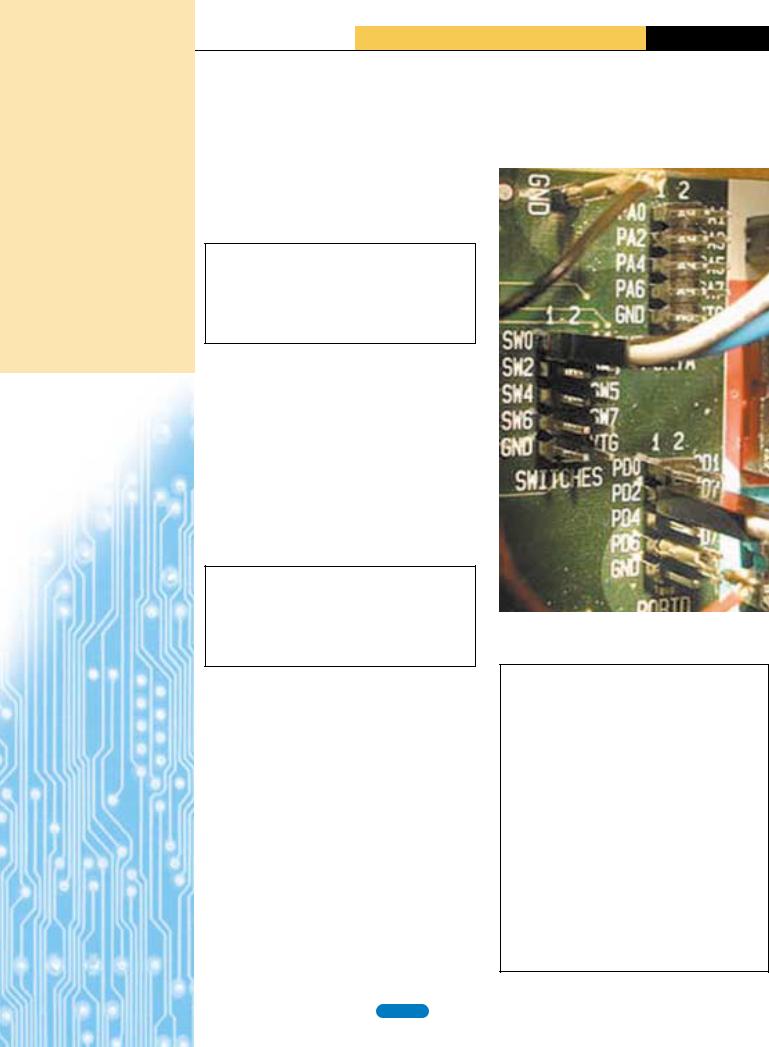
...and again; the only thing you really need to know for this little tutorial; is the position of one special little bit: this one is called "Timer/Counter0 Overflow Interrupt enable", abbreviated "TOIE0" and found in bit postition
1 of this register.
A T M E L A P P L I C A T I O N S J O U R N A L
You are very able to read this now, and realize that it is just like the previous .org's in this program. Let's move on!
TIMSK, TCCR0,TCNT0
Together, these 3 registers are all we need consider to have timing interrupts in an application on the AVR.
TCCR0 controls the operation of Timer/counter 0. The count is incremented for every clock signal at the input of the timer. But the clock input can be selected, and prescaled by N. We'll just consider the 3 lowest bits of this register:
TCCR0 |
|
|
|
|
Timer/Counter0 register |
|||
Bit |
7 |
6 |
5 |
4 |
3 |
2 |
1 |
0 |
|
- |
- |
- |
- |
- |
CS02 |
CS01 |
CS00 |
Read/write |
R |
R |
R |
R |
R |
R/W |
R/W |
R/W |
Init. value |
0 |
0 |
0 |
0 |
0 |
0 |
0 |
0 |
Note that bits 7-3 are reserved, and always read as zero
This table shows the different settings of these 3 control bits:
CS02 |
CS01 |
CS00 |
Description |
0 |
0 |
0 |
Stop the timer/counter |
0 |
0 |
1 |
CK |
0 |
1 |
0 |
CK/8 |
0 |
1 |
1 |
CK/64 |
1 |
0 |
0 |
CK/256 |
1 |
0 |
1 |
CK/1024 |
1 |
1 |
0 |
Ext. pin T0, falling edge |
1 |
1 |
1 |
Ext. pin T0, rising edge |
|
|
|
|
TIMSK; the Timer/Counter Interrupt Mask register is simply a "mask" register for enabling/disabling interrupts just like you have already seen with the GIMSK register:
TIMSK |
|
Timer/Counter Interrupt Mask register |
||||||
Bit |
7 |
6 |
5 |
4 |
3 |
2 |
1 |
0 |
|
TOIE1 |
OCIE1A |
OCIE1B |
- |
TICIE1 |
- |
TOIE0 |
- |
Read/write |
R/W |
R/W |
R/W |
R |
R/W |
R |
R/W |
R |
Init. value |
0 |
0 |
0 |
0 |
0 |
0 |
0 |
0 |
Note that bits 4,2 and 0 are reserved, and always read as zero
...and again; the only thing you really need to know for this little tutorial; is the position of one special little bit: this one is called "Timer/Counter0 Overflow Interrupt enable", abbreviated "TOIE0" and found in bit postition 1 of this register. To enable our Timer interrupt; set this bit (to "1"). TCNT0 is the actual "Timer/Counter" register. This is where the timing and counting is done, in accordance with the settings in TCCR0. This is simply a register for storing a counter value; there are no special bits in it. It is entirely readable/writable; so you can load it with any desired starting value for your counting if you like. Note that it does not reset itself automatically, even if an interrupt is issued.
This is already becoming old news to you now, since it's just more or less another instance of registers controlling similar functions that you have already heard about regarding the external interrupts... So let's go right to the code>.
Real code part 2
For illustrating the Timer0 Overflow interrupt; we connect a small speaker to an output pin of the 8515. Each Timer0 overflow interrupt will toggle the pin. The result is that the speaker will buzz with a base frequency proportional to the frequency with which the pin is toggled. I.e. the base frequency will be:
CLK/2*Prescale*(256-TIME)
where TIME is the current value in the TIME register (r16).
Also, the two switches affecting the value in TIME will make the buzz frequency waver up or down.
The picture shows how to connect the speaker. We have chosen pin PD6 for no particular reason.
Huh? |
Why is that the formula for the base frequency? |
?The Timer/counter counts up from some value every clock cycle until it overflows. Then we reset it, to repeat the drill.
Let's say the timer can only count to 1 before overflow. Flipping the pin every time, will give us one cycle of a squarewave like waveform every 2 flips, right? (up a while, then down a while, repeat...). Hence, the base frequency would be:
CLK/2
Now; the Timer/Counter register is 8 bits wide, and can count from any value it is set (TIME) to 255. The formula becomes:
CLK/2*(256-TIME)
Besides; we have a prescaler which, when set to N, makes the Timer count just every Nth cycle...
CLK/2*N*(256-TIME)
www.atmel.com
page 16

A T M E L A P P L I C A T I O N S J O U R N A L
Now, these were the very basic basics of interrupts and I/O. Feel free to experiment with what you have learnt in this article; use other prescaler settings, try other flanks of external interrupt triggering, write programs that use switches to make flow control decisions, whatever...
Good luck!
These are the three snippets of code to insert. Please consult the complete |
ing every bit in BEEP (r18) with the com instruction, and then OR'ing it with |
||
source code (INTs_2.asm, available below) to where the snippets are insert- |
this value 0xbf = 10111111 b (note the 6th position is '0'). |
||
ed: |
|
|
|
|
|
|
|
INTs_2.asm |
|
|
Source snippets for second part of program |
(~3kB) |
;------------------ |
CODE SNIPPET #1 - OVF0addr vector ----------------------------- |
|
; inserted below the existing vector defs |
|||
|
;----------------------------------------------------------------------------------- |
|
|
|
.org OVF0addr |
|
|
|
rjmp |
TimerV0 |
; T/C0 overflow vector |
|
. |
|
|
|
. |
|
|
|
;------------------ |
CODE SNIPPET #2 - Initializing TIMSK,TCCR0,TCNT0 ------------- |
|
|
; inserted in the Reset: label, right before the 'sei' call |
||
|
;---------------------------------------------------------------------------------- |
|
|
|
ldi |
TIME,$80 |
; Start from 128. NB! |
|
out |
TCNT0,TIME |
; set Timer/counter also. |
|
ldi |
TEMP,(1<<TOIE0) |
; timer overflow interrupt enable 0 |
|
out |
TIMSK,TEMP |
|
|
ldi |
TEMP,$02 |
; clock prescaler = clk/8 |
|
out |
TCCR0,TEMP |
|
|
. |
|
|
|
. |
|
|
|
;---------- |
CODE SNIPPET #3 - handling the Timer overflow int. -- |
|
|
; new subroutine label, inserted at the end of the file |
||
|
;---------------------------------------------------------------- |
|
|
|
TimerV0: |
|
|
|
out |
TCNT0,TIME |
; reset time |
|
com |
BEEP |
|
|
ori |
BEEP,$BF |
; bit 6 only |
|
out |
PORTD,BEEP |
|
|
reti |
|
; important! |
|
|
|
|
;---------- CODE SNIPPET #1 - OVF0addr vector -------------------
This part simply declares the Timer Overflow vector address.
;---------- CODE SNIPPET #2 - Initializing TIMSK,TCCR0,TCNT0 ----
First, we set the TIME register to a higher value (0x80 = 128 decimal) for starters, and load it into the Timer/Counter register. It's just a more fitting start value if you run the 8515 on a low CLK freq. Then the relevant interrupt enable bit is set in the TIMSK register, and the prescaling bits in the Timer Control register are set to Prescale=8.
This way, if the 8515 runs @ 1.23MHz; the speaker will buzz with a base frequency equal to 1.23E6/2*8*127 = 605.3 Hz
; ---------- CODE SNIPPET #3 - handling the Timer overflow int. -- The important issues in handling this interrupt is:
•Resetting the Timer/Counter - it won't do that itself!
•Flipping the beep pin
•Returning to the program
Resetting Timer/Counter is obviously done by loading the value of TIME (r16) into TCNT0, and returning from the interrupt routine is done by issuing a reti instruction.
Flipping the beep pin (PD6) is a little curious, however: This is done by invert-
BEEP |
00000000 |
after com: |
11111111 |
'OR' with: |
10111111 |
Result: |
11111111 |
after com: |
00000000 |
'OR' with: |
10111111 |
Result: |
10111111 |
etc... |
... |
As you may see; whichever value is in BEEP, the 6th bit of it will flip every time... So, the pin will toggle up and down, and the speaker beeps this little song: "...10101010101010...". Haha.
Now, these were the very basic basics of interrupts and I/O. Feel free to experiment with what you have learnt in this article; use other prescaler settings, try other flanks of external interrupt triggering, write programs that use switches to make flow control decisions, whatever...
Good luck!
www.atmel.com
page 17

A T M E L A P P L I C A T I O N S J O U R N A L
The Atmel megaAVR devices are designed for flexible use with a lot of powerful peripherals which limit the need of external components. These devices are well designed, and the peripherals can be set-up in many different ways to support many different application needs. Because of
the flexibility in the microcontroller, it is necessary to set up the pins in the way your specific board is designed, and also to set the operation of the peripherals according to your product needs.
www.atmel.com
Device Drivers and the
Special Function Register Hell
By Evert Johansson, IAR Systems
Using the built-in power of the microcontroller
A modern microcontroller has a lot of peripherals, and it is a time-consuming part of each embedded project to write the code needed to use that builtin power and flexibility. It is a tedious work to read the hardware manual and understand how peripheral modules like I/O, timers, USART, etc are implemented, and how the software is to get access to the hardware. Each peripheral is controlled via a number of special function registers where each bit has a special meaning, and many of
these bits need to be written and read using a specific protocol.
Atmel megaAVR
The Atmel megaAVR devices are designed for flexible use with a lot of powerful peripherals which limit the need of external components. These devices are well designed, and the peripherals can be set-up in many different ways to support many different application needs. Because of the flexibility in the microcontroller, it is necessary to set up the pins in the way your specific board is designed, and also to set the operation of the peripherals according to your product needs. For instance, the I/O input/output pins are multiplexed with peripheral pins, and need to be initialized according to
the hardware implementation.
Application notes
One way to speed up the set up and coding is to use software application notes, which help to use the peripheral. The drawback with application notes is that you do not have the same requirements for your product as the engineer who wrote the application note. Therefore, you need to update the special function register settings manually, and you might also need to modify the application note source code to suit your needs.
Software analysis
If device driver software written for different products is analysed, you will see that most of these drivers are written in much the same way. The reason for this is that the microcontroller is designed in a particular way, and therefore the access to the special function register bits, such as control/status and data bits, needs to be done in a certain way. This actually means that a lot of engineers are writing the same kind of software for different products over and over again. Writing the same kind of software at different places will also need a lot of extra testing to verify that the code runs correctly in the hardware.
The special function register Hell
Microcontrollers include hundreds of special function registers placed at certain addresses in the address space, and it is common that a register is made up of many bitfields or bits. This means that the application needs to access or control thousands of bits, and the access needs to be performed in the way the microcontroller is designed for. Therefore, the productivity for modelling and writing device driver software is normally four times lower than ordinary software coding.
Some registers or bits are both readand write-accessible, while others are only accessible via read, write, set, or clear. It is also common that registers need to be accessed via a specific protocol. Sometimes the register or bit needs to be read by the software before it can be updated with a write, set, or clear instruction. Some registers are also related to each other, so that one register
bit needs to be set or cleared in a register before a bit in the corresponding register can be read or updated.
Get your product to the market quickly
IAR MakeApp for Atmel megaAVR is a tool that guides you through the special function register hell, and helps you with the writing of device drivers. This new low-cost product from IAR Systems includes property dialog boxes which make it easy to configure the megaAVR microcontroller to suit your needs. IAR MakeApp warns you if you try to make a setting that will occupy an already used resource, e.g. the same I/O pin. The product also presents a visual view of the microcontroller and how the pins are configured. Special function register values are calculated automatically according to your settings, and a complete set of device drivers can be generated. The product also includes a component browser and a project report generation function that helps you with the design and documentation.
Device drivers generated by IAR MakeApp
IAR MakeApp contains a powerful code generation technology, and generates a complete set of customized device driver functions according to your project settings. The code generation engine uses the component database information, and automatically calculates the special function register values according to the current property settings. ANSI C source code is generated for each peripheral, and the files are well commented and easy to follow. The drivers include initialization, run-time control, and interrupt handling functions. The functions are ready to be used by your application software and tested with IAR Embedded Workbench for AVR and the Atmel STK500 starter kit. Use IAR MakeApp from Idea to Target. “Click & Go” for driver variants during all phases of your embedded project.
Example: IAR MakeApp USART configuration, code generation, and usage
ATmega128 includes two USART channels for serial communication.
1.Open the USART property dialog box in IAR MakeApp.
2.Make the settings for the channel your hardware is designed for, and make the following minimum selection: Select operating mode, activate USART receive/transmit pins, set baud rate, and define your protocol (number of data bits, parity, and stop bits). Finally, choose if you want to use interrupts.
3.At any time you can view the special function register settings by clicking the Registers button in the property dialog box.
4.The output generation tab in the USART property dialog box includes the device driver functions for USART that will be generated according to your current settings. The device drivers (APIs) for channel 0 normally include the following functions: MA_InitCh0_USART(), MA_ResetCh0_USART(), MA_PutCharCh0_USART(), MA_PutStringCh0_USART(), MA_GetCharCh0_USART(), MA_GetStringCh0_USART(), MA_IntHandler_RX0_USART(), MA_IntHandler_TX0_USART(), MA_IntHandler_UDRE0_USART().
If your application software will only use some of these functions, you can choose to have only these ones generated by the tool.
5.Click OK to save the settings.
continued on page 40
page 18