

CIR V1
.0.pdfData Value |
Data Bit Set |
16PSM Data |
|||
(Hex) |
|
(DBS) |
|
Symbol |
|
|
|
|
|
|
|
0x0 |
0 |
0 |
0 |
0 |
1 0 1 0 0 0 0 0 |
0x1 |
0 |
0 |
0 |
1 |
0 1 0 1 0 0 0 0 |
0x2 |
0 |
0 |
1 |
0 |
0 0 1 0 1 0 0 0 |
0x3 |
0 |
0 |
1 |
1 |
0 0 0 1 0 1 0 0 |
0x4 |
0 |
1 |
0 |
0 |
0 0 0 0 1 0 1 0 |
0x5 |
0 |
1 |
0 |
1 |
0 0 0 0 0 1 0 1 |
0x6 |
0 |
1 |
1 |
0 |
1 0 0 0 0 0 1 0 |
0x7 |
0 |
1 |
1 |
1 |
0 1 0 0 0 0 0 1 |
0x8 |
1 |
0 |
0 |
0 |
1 1 1 1 0 0 0 0 |
0x9 |
1 |
0 |
0 |
1 |
0 1 1 1 1 0 0 0 |
0xA |
1 |
0 |
1 |
0 |
0 0 1 1 1 1 0 0 |
0xB |
1 |
0 |
1 |
1 |
0 0 0 1 1 1 1 0 |
0xC |
1 |
1 |
0 |
0 |
0 0 0 0 1 1 1 1 |
0xD |
1 |
1 |
0 |
1 |
1 0 0 0 0 1 1 1 |
0xE |
1 |
1 |
1 |
0 |
1 0 1 0 0 1 0 1 |
0xF |
1 |
1 |
1 |
1 |
1 1 1 0 0 0 0 1 |
Table 3.1: 16PSM Data Symbol Representation
Since the transmission speed in the IrDA Control system is 75.0 kbps, symbol time Dt and chip time Ct are given with the following equations:
Dt = 4 * (1 / 75000)
=53.33 [μs] Ct = 53.33E-6 / 8
=6.67 [μs]
The 16PSM scheme, using this specific symbols set, has low energy in the frequency band of around 33kHz to 40kHz, which is the frequency band used for Remote Control Systems (see Figure 3.2). The spectrum characteristics of the IrDA Control signal based on the 16PSM scheme are shown in Appendix A.
3.2.2 PHY Packet Structure
The IrDA Control packet format is shown in Figure 3.3. There are two packet formats in the IrDA Control system; short packets and long packets. Each packet consists of six fields: the Automatic Gain Control (AGC); Preamble (PRE); Start Flag (STA or STL); MAC frame; Cyclic Redundancy Check (CRC which can be CRC-8 or CRC-16); and Stop Flag (STO) fields.
IrDA CIR Standard |
June 30, 1998 |
11 |

AGC |
PRE |
STA |
|
CRC |
STO |
|
|
= STS |
MAC frame |
= CRC – 8 |
|
(2 bit times) |
(5 bit times) |
(5 bit times) |
|
(8 bits) |
(4 bit times) |
|
|
|
(a) Short Packet |
|
|
|
|
|
|
|
|
AGC |
PRE |
STA |
|
CRC |
STO |
|
|
= STL |
MAC frame |
= CRC–16 |
|
(2 bit times) |
(5 bit times) |
(5 bit times) |
|
(16 bits) |
(4 bit times) |
|
|
|
(b) Long Packet |
|
|
Figure 3.3: IrDA Control Packet Format
The pulse sequence for each of AGC, PRE, STS, STL, and STO fields is shown in Table3.2. The chips are transmitted starting with the leftmost bit in each field; time moves from left to right.
|
|
Field Name |
Pulse Sequence |
||||
|
|
|
|
|
|
|
|
|
|
|
|
AGC |
1 1 1 1 |
|
|
|
|
|
|
|
|
|
|
|
|
|
|
PRE |
0 1 0 1 0 1 0 1 0 1 |
||
|
|
|
|
|
|
|
|
|
|
|
|
STS |
0 1 1 0 1 1 0 1 0 0 |
||
|
|
|
|
|
|
|
|
|
|
|
|
STL |
0 1 0 0 1 0 1 1 0 1 |
||
|
|
|
|
STO |
0 1 0 0 1 0 1 1 |
||
|
|
|
|
|
|
|
|
First chip delivered to/received |
|
|
|
|
|
||
|
by physical layer |
|
|
|
|
|
|
|
|
|
|
|
|
||
|
|
|
|
|
|
|
|
|
|
|
|
|
|
||
|
Last chip delivered to/received |
|
|
|
|||
|
by physical layer |
|
|
|
|||
|
|
|
|
||||
|
|
|
|
|
|
|
|
Table 3.2: Pulse Sequence Representation for AGC, PRE, STS, STL, and STO
For a short packet, STS/CRC-8 is used as STA/CRC. For a long packet, STL/CRC-16 is used as STA/CRC. The details of the CRC field will be described in Section 3.2.3.
The AGC field is used to control the gain and/or threshold level of the infrared receiver. The PRE field is used to get chip (clock) synchronization. The STA field is used to get symbol synchronization, and to indicate a short (STS) or long (STL) packet. The STO field is used to indicate the end of the packet.
As shown in Section 3.2.1, 16PSM has the regularity that a chip of logical “1” appears only twice or four times during the eight possible chip slots and that the combination of logical “0” and ”1” in a symbol is restricted to 16 patterns shown in Table.3.1. Since the AGC, PRE, STA, and STO fields use pulse sequences that violate this regularity, there is no need for a bit stuffing mechanism in the 16 PSM coding scheme. This modulation scheme allows the time for a packet to be transmitted to be determined without dependence on the data contents. This is an advantage of 16 PSM coding in comparison with some other coding schemes. It can also be an advantage in implementing critical latency applications.
3.2.3 CRC Field
The CRC field is 8 or 16 bits in length for a short packet or a long packet, respectively. It contains a value computed over the entire MAC frame field.
A CRC-8 consists of the 16 PSM encoded data resulting from the CRC-8 algorithm for cyclic redundancy check as applied to the data contained in the packet. The CRC-8 polynomial is x8 + x7 + x2 +1. The data bytes are input to this
IrDA CIR Standard |
June 30, 1998 |
12 |
calculation in LSB first format. The CRC-8 calculated result for each packet is treated as one data byte, and the byte is encoded in the same manner as the data bytes in MAC frame.
A CRC-16 consists of the 16PSM encoded data resulting from the CRC-16 algorithm for cyclic redundancy check as applied to the data contained in the packet. The CRC-16 polynomial is x16 + x15 + x2 +1. The data bytes are input to this calculation in LSB first format. The CRC16 calculated result for each packet is treated as two data bytes, and each byte is encoded in the same manner as the data bytes in MAC frame.
The CRC register is preset to all "1's" prior to calculation of the CRC on the transmit data stream. When data has ended and the CRC is being shifted for transmission at the end of the packet, a "0" should be shifted in so that the CRC register becomes a virtual shift register. Note: the inverse of the CRC register is what is shifted as defined in the polynomial.
3.2.4 Procedure for Transmitting Data Packet
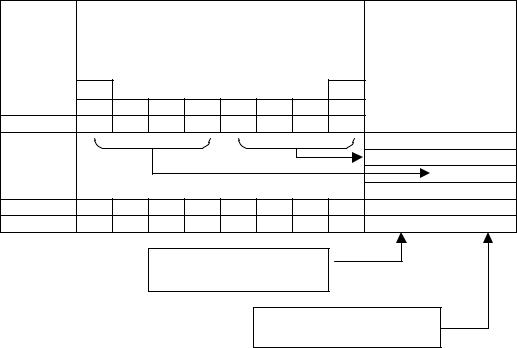
The procedure for creating a data transmission packet is described below (Figure 3.4):
|
|
|
|
|
|
|
|
|
Resulting 16 PSM data |
|
|
|
|
|
Resulting DBSs |
|
|
|
symbol streams (chips |
||
Data Value |
|
|
|
|
|
|
|
|
and symbols transmitted |
|
(Byte) |
|
|
|
|
|
|
|
|
from left to right for LSB |
|
|
|
|
|
|
|
|
|
|
first reception) |
|
|
MSB |
|
|
|
|
|
|
LSB |
|
|
|
D7 |
D6 |
D5 |
D4 |
D3 |
D2 |
D1 |
D0 |
|
|
0x1B |
0 |
0 |
0 |
1 |
1 |
0 |
1 |
1 |
|
|
|
|
|
|
|
|
|
|
|
00011110 |
|
|
|
|
|
|
|
|
|
|
|
01010000 |
|
|
|
|
|
|
|
|
|
00011110 |
01010000 |
0x0B |
0 |
0 |
0 |
0 |
1 |
0 |
1 |
1 |
00011110 |
10100000 |
0xF5 |
1 |
1 |
1 |
1 |
0 |
1 |
0 |
1 |
00000101 |
11100001 |
|
|
|
First chip delivered to/received |
|
|
|
||||
|
|
|
|
|
by physical layer |
|
|
|
||
Last chip delivered to/received by physical layer
Figure 3.4: Example of packet generation procedure
(1)Each data byte [D7 – D 0] in the original data which is included in the MAC frame and CRC fields is divided into two Data Bit Sets (DBSs), [D7 – D 4] and [D3 – D 0]. The DBSs are converted into the corresponding 16PSM Data Symbols in the order of [D3 – D 0] and [D7 – D 4] in Table 3.1.
(2)The AGC, PRE and STA fields are added to the head of the resulting stream of 16PSM data symbols in the above step and the STO to the tail of that stream.
3.3 Modulation
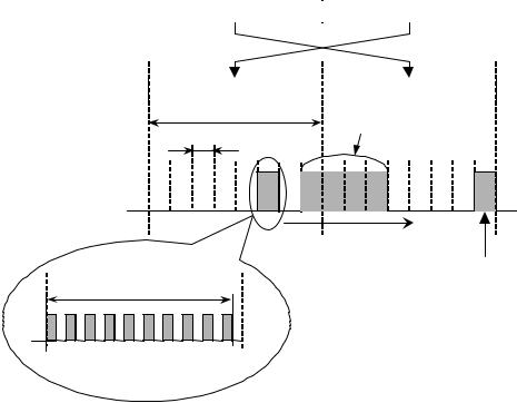
Corresponding to logic “0” or “1” in the packet generated by the procedure in Section 3.2.4, the infrared transmitter outputs the subcarrier signal for a chip of logic “1”, and outputs no signal for a chip of logic “0”. The relation between the data to be transmitted and the waveform output by the infrared transmitter is shown in Figure 3.5.
IrDA CIR Standard |
June 30, 1998 |
13 |
Data Value = 0xF5 |
|
|
1 |
1 |
1 |
1 |
|
|
|
|
0 |
1 |
0 |
1 |
|
|
(Byte) |
|
|
|
|
|
|
|
|
|
|
|
|
|
|
|
|
|
|
|
|
|
|
|
|
|
|
|
|
|
|
|
|
|
|
|
|
|
|
|
|
|
|
|
|
|
|
|
|
|
|
0 |
0 |
0 |
0 |
0 |
1 |
0 |
1 |
1 |
1 |
1 |
0 |
0 |
0 |
0 |
1 |
|
|
|
|
|
|
|
|
|
|
|
|
|
|
|
|
|
|
Symbol
successive SEPCs
Chip
IRBus Signal
|
Increasing time |
|
subcarrier emission |
subcarrier emission pulse chip (SEPC) |
|
pulse duration (SEPD) |
||
|
10 subcarriers / SEPC
Figure 3.5 : Waveform Example of IRBus Signal
The chip for which the infrared transmitter outputs the subcarrier signal is defined as a subcarrier emission pulse chip (SEPC). For example, when the original data is “0xF5”, four successive SEPCs appear over two adjacent symbols, and the infrared transmitter continuously outputs the subcarrier for the duration of the four chips (fourfold chips), as shown in Figure 3.5. The duration between the rising edge of the initial subcarrier and the falling edge of the final subcarrier in the successive SEPCs is defined as subcarrier emission pulse duration (SEPD). Time is measured at the 50% point of the subcarrier amplitude.
The number of subcarriers included in each SEPD of Single, Double, Triple, Fourfold, Fivefold, Sixfold, Sevenfold and Eightfold Chips is 10, 20, 30, 40, 50, 60, 70 and 80, respectively. The infrared transmitter must synchronize the subcarrier with the SEPCs such that the number of subcarrier pulses is entirely included in each SEPD.
IrDA CIR Standard |
June 30, 1998 |
14 |
3.4 Overall Link Specifications
The specifications of the overall link are shown in Table 3.3.
Specification |
|
Minimum |
Typical |
Maximum |
Unit |
Maximum Link Length |
|
|
|
|
|
Between Host and Peripheral Type1 Devices |
5.00 |
|
|
m |
|
Host Devices ( θH<+/-30deg and φH=0) |
|
|
|
|
|
Peripheral Type 1 Devices ( θP<+/-15deg and φP=0) * |
|
|
|
|
|
Between Host and Peripheral Type1 Devices |
3.00 |
|
|
m |
|
Host Devices (θH<+/-50deg and φH=0) |
|
|
|
|
|
Peripheral Type 1 Devices (θP<+/-15deg and φP=0) * |
|
|
|
|
|
Between Host and Peripheral Type1 Devices |
5.00 |
|
|
m |
|
Host Devices ( θH=0 and φH<+/-15deg) |
|
|
|
|
|
Peripheral Type 1 Devices ( θP=0 and φP<+/-15deg) * |
|
|
|
|
|
Between Host and Peripheral Type2 Devices |
1.50 |
|
|
m |
|
Host Devices ( θH<+/-40deg and φH=0) |
|
|
|
|
|
Peripheral Type2 Devices ( θP<+/-40deg and φP=0) * |
|
|
|
|
|
Between Host and Peripheral Type2 Devices |
1.50 |
|
|
m |
|
Host Devices ( θH=0 and φH<+/-25deg) |
|
|
|
|
|
Peripheral Type 2 Devices ( θP=0 and φP<+/-25deg) * |
|
|
|
|
|
Minimum Link Length |
|
|
|
|
|
Between Host and Peripheral Type1 Devices |
|
|
0.20 |
m |
|
Host Devices ( θH<+/-50deg and φH=0) |
|
|
|
|
|
Peripheral Type 1 Devices ( θP<+/-15deg and φP=0) * |
|
|
|
|
|
Between Host and Peripheral Type1 Devices |
|
|
0.20 |
m |
|
Host Devices ( θH=0 and φH<+/-15deg) |
|
|
|
|
|
Peripheral Type 1 Devices ( θP=0 and φP<+/-15deg) * |
|
|
|
|
|
Between Host and Peripheral Type2 Devices |
|
|
0.20 |
m |
|
Host Devices ( θH<+/-40deg and φH=0) |
|
|
|
|
|
Peripheral Type2 Devices ( θP<+/-40deg and φP=0) * |
|
|
|
|
|
Between Host and Peripheral Type2 Devices |
|
|
0.20 |
m |
|
Host Devices ( θH=0 and φH<+/-25deg) |
|
|
|
|
|
Peripheral Type 2 Devices ( θP=0 and φP<+/-25deg) * |
|
|
|
|
|
Peak Wavelength |
(All Devices) |
850 |
|
900 |
nm |
Duty of Subcarrier |
(All Devices) |
47.5 |
50.0 |
52.5 |
% |
Subcarrier Emission Pulse Duration |
(All Devices) |
|
|
|
|
( for Single Chip ) |
|
6.23 |
6.33 |
6.44 |
μs |
( for Double Chip ) |
|
12.82 |
13.00 |
13.18 |
μs |
( for Triple Chip ) |
|
19.42 |
19.67 |
19.92 |
μs |
( for Fourfold Chip ) |
|
26.01 |
26.33 |
26.66 |
μs |
( for Fivefold Chip ) |
|
32.60 |
33.00 |
33.40 |
μs |
( for Sixfold Chip ) |
|
39.20 |
39.67 |
40.14 |
μs |
( for Sevenfold Chip ) |
|
45.79 |
46.33 |
46.89 |
μs |
( for Eightfold Chip ) |
|
52.39 |
53.00 |
53.63 |
μs |
Rise Time Tr,10-90%,Fall Time Tf,90-10% (All Devices) |
|
|
80 |
ns |
|
Optical Over Shoot |
(All Devices) |
|
|
25 |
% |
Edge Jitter (Peak to Peak) |
(All Devices) |
|
|
20 |
ns |
*: See Figure 3.6
Table 3.3: Overall link Specifications
IrDA CIR Standard |
June 30, 1998 |
15 |

The required link length and directivity angle can vary depending on applications. For example, the link length that is required for a remote control unit is different from that for a desktop mouse. In the IrDA Control specification two types of peripheral devices for long and short distances are defined.
An IrDA Control system must satisfy a communication quality of BER=10-4 within the range of the following link length under a 20% IrDA sunlight ambient (=100μW/cm2).
Each angle in Table 3.3 is illustrated in Figure 3.6. θΗ is the horizontal angle between the host’s transceiver’s plane normal and the line that includes both of the transceivers of the host and the peripheral. θP is the horizontal angle between the peripheral’s transceiver’s plane normal and the line that includes both of the transceivers of the host and the peripheral. φΗ is the vertical angle between the host’s transceiver’s plane normal and the line that includes both of the transceivers of the host and the peripheral. φP is the vertical angle between the peripheral’s transceiver’s plane normal and the line that includes both of the transceivers of the host and the peripheral.
19:05
Host
|
|
|
|
|
|
θH |
|
Host |
|
φH |
||||||
|
|
|
|
|
|
|
||||||||||
|
|
|
|
|
|
|
|
|
|
|
|
|
|
|
|
|
|
|
|
|
|
|
|
|
|
|
|
|
|
Peripheral |
|||
|
|
|
|
|
|
|
|
|
|
|
|
|
||||
|
|
|
|
|
|
|
|
|
|
|
|
|
||||
|
|
|
|
|
|
|
|
|
|
|
|
|
|
|
|
|
|
|
|
|
|
|
|
|
|
|
|
|
|
φP |
|
|
|
|
|
|
|
|
|
|
θP |
|
|
|
|
|
||||
|
|
|
|
|
|
|
|
|
|
|
|
|
|
|
||
|
|
|
|
|
|
|
Peripheral |
|
|
|
|
|
|
|
|
|
|
Top View |
|
|
|
|
Side View |
||||||||||
θH: Horizontal Angle ( Host ) |
φH : Vertical Angle ( Host ) |
|||||||||||||||
θP : Horizontal Angle ( Peripheral ) |
φP : Vertical Angle ( Peripheral ) |
|||||||||||||||
Figure 3.6: Definitions of Angles
IrDA CIR Standard |
June 30, 1998 |
16 |
The peak wavelength specification of the infrared radiation shall be the same as that in the IrDA 1.1 system (Reference 2).
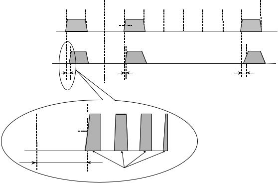
As shown in Figure 3.7, Leading Edge Jitter is the deviation between time positions of the actual leading edge and the expected leading edge of the first subcarrier in the successive SEPCs. The expected leading edge time can be calculated from the average chip period within the preceding 16 bit times. Peak to peak Leading Edge Jitter is the difference between the maximum and minimum occurrences. The leading edge time position is measured at the 50% point of the amplitude of the first subcarrier in the successive SEPCs.
Trailing Edge Jitter is the deviation between time positions of the actual trailing edge and expected trailing edge of the last subcarrier in the successive SEPCs. The expected trailing edge time can be calculated from the average chip period within the preceding 16 bit times. Peak to peak Trailing Edge Jitter is the difference between the maximum and minimum occurrences. The trailing edge time position is measured at the 50% point of the amplitude of the last subcarrier in the successive SEPCs.
Edge Jitter is defined as the larger one of Leading Edge Jitter and Trailing Edge Jitter.
Expected Transmitted |
50% |
|
Signal |
||
|
Actual Transmitted
Signal
deviation Ei |
deviation Ei+1 |
Jitter = Max(Ei) - Min(Ej) ( 1<= i,j<= N)
100%


50%
deviation Ei-1 |
subcarrier |
|
Figure 3.7 : Definition of Jitter |
IrDA CIR Standard |
June 30, 1998 |
17 |
The subcarrier emission pulse duration (SEPD) is defined in Section 3.3. The minimum value of SEPD is given by the following equation, using the maximum subcarrier frequency specified in Section 3.5 and 3.6, the number of subcarriers included in each SEPD, the minimum duty of subcarrier, and the maximum edge jitter:
|
Ns − ( 1 − Dsmin. ) |
|
Ns : number of subcarriers included in each SEPD |
||
SEPDmin. = |
− Jemax. |
Ds : duty of subcarrier |
|||
fs |
: subcarrier frequency |
||||
|
|||||
|
fsmax. |
Je |
: edge jitter |
||
The maximum value of SEPD is given by the following equation, using the minimum subcarrier frequency specified in Section 3.5 and 3.6, the number of subcarriers included in each SEPD, the maximum duty of subcarrier and the maximum edge jitter:
SEPDmax . = Ns − ( 1 − Dsmax . ) + Jemax .
fsmin .
Ns : number of subcarriers included in each SEPD Ds : duty of subcarrier
fs : subcarrier frequency Je : edge jitter
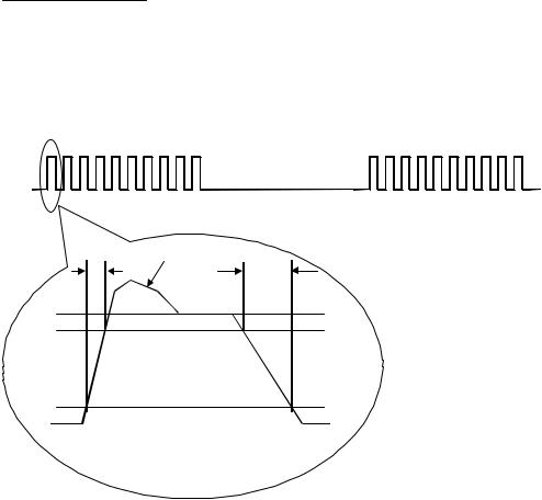
Rise Time Tr, Fall Time Tf and Overshoot can be defined for a single subcarrier pulse. Since overshoot is referenced to the pulse amplitude at the end of the subcarrier pulse. For Rise Time Tr, Fall Time Tf and Overshoot is given in Figure 3.8.
IRBus Signal
|
Overshoot |
T |
T |
r |
f |
100%
90%
10%
0%
Figure 3.8: Definitions of Tr ,Tf and Overshoot
IrDA CIR Standard |
June 30, 1998 |
18 |
3.5 IR Output Interface Specifications
The IrDA Control infrared transmitter must satisfy the IR output interface specification shown in Table 3.4.
Specification |
Minimum |
Typical |
Maximum |
Unit |
Intensity |
|
|
|
|
Host Devices ( θH<+/-30deg and φH=0 ) * |
100 |
|
500 |
mW/sr |
Host Devices ( θH<+/-40deg and φH=0 ) * |
68 |
|
500 |
mW/sr |
Host Devices ( θH<+/-50deg and φH=0 ) * |
36 |
|
500 |
mW/sr |
Host Devices ( θH=0 and φH<+/-15deg ) * |
100 |
|
500 |
mW/sr |
Host Devices ( θH=0 and φH<+/-25deg ) * |
20 |
|
500 |
mW/sr |
Peripheral Type 1 Devices ( θP<+/-15deg and φP=0) * |
100 |
|
500 |
mW/sr |
Peripheral Type 1 Devices ( θP=0 and φP=<+/-15deg ) * |
100 |
|
500 |
mW/sr |
Peripheral Type 2 Devices ( θP<+/-40deg and φP=0) * |
9 |
|
500 |
mW/sr |
Peripheral Type 2 Devices ( θP=0 and φP=<+/-25deg) * |
9 |
|
500 |
mW/sr |
Signaling Rate |
|
|
|
|
Host Devices |
74.925 |
75.0 |
75.075 |
kbps |
Peripheral Type 1 Devices |
74.175 |
75.0 |
75.825 |
kbps |
Peripheral Type 2 Devices |
74.175 |
75.0 |
75.825 |
kbps |
Subcarrier Frequency |
|
|
|
|
Host Devices |
1.4985 |
1.50 |
1.5015 |
MHz |
Peripheral Type 1 Devices |
1.4835 |
1.50 |
1.5165 |
MHz |
Peripheral Type 2 Devices |
1.4835 |
1.50 |
1.5165 |
MHz |
*: See Figure 3.6.
Table 3.4: IR Output Interface Specifications
The tolerance of the signaling rate and subcarrier frequency for host devices, peripheral type 1 devices and peripheral type 2 devices are +/- 0.1%, +/- 1.1% and +/- 1.1% of their typical value, respectively.
Figure 3.9 shows the Intensity in angular range in horizontal plane for respective devices. For angles of any degree, the intensity should be equal to or less than the maximum intensity. In addition, within the defined angular range, the intensity should be equal to or more than the minimum intensity.
IrDA CIR Standard |
June 30, 1998 |
19 |
|
|
Intensity [ mW/sr ] |
|
|
|
|
|
|
|
500 |
Unacceptable Region |
||
a) Host Devices |
|
|
Acceptable Region |
|||
|
|
|
100 |
|
|
|
|
|
|
68 |
|
|
|
|
|
|
36 |
|
|
|
-50 |
40 |
30 |
0 |
30 |
40 |
50 |
|
|
Angle [degrees] |
|
|
|
|
|
|
Intensity |
[ mW /sr ] |
|
|
|
|
|
|
500 |
Unacceptable Region |
||
b) Peripheral Type 1 Devices |
Acceptable Region |
|||||
|
|
|
|
|||
Unacceptable |
|
100 |
|
|
|
|
Region |
|
|
|
|
|
|
|
|
|
|
|
|
|
|
|
-15 |
0 |
15 |
|
|
|
|
Angle [degrees] |
|
|
|
|
|
|
Intensity |
[ mW / sr ] |
|
|
|
|
|
|
500 |
Unacceptable Region |
||
c) Peripheral Type 2 Devices |
Acceptable Region |
|||||
|
|
|
||||
-40 |
0 |
40 |
|
Angle [degrees] |
|
Figure 3.9: Acceptable Intensity Region in horizontal angular range
IrDA CIR Standard |
June 30, 1998 |
20 |