

Микропроцессорная техника Сторожок / Datasheet.hk_dspic33fj32mc204_1234824
.pdfdsPIC33FJ32MC202/204 and dsPIC33FJ16MC304 Data Sheet
High-Performance,
16-bit Microcontrollers
♥ 2007 Microchip Technology Inc.
Preliminary |
DS70283B |

Note the following details of the code protection feature on Microchip devices:
•Microchip products meet the specification contained in their particular Microchip Data Sheet.
•Microchip believes that its family of products is one of the most secure families of its kind on the market today, when used in the intended manner and under normal conditions.
•There are dishonest and possibly illegal methods used to breach the code protection feature. All of these methods, to our knowledge, require using the Microchip products in a manner outside the operating specifications contained in Microchip’s Data Sheets. Most likely, the person doing so is engaged in theft of intellectual property.
•Microchip is willing to work with the customer who is concerned about the integrity of their code.
•Neither Microchip nor any other semiconductor manufacturer can guarantee the security of their code. Code protection does not mean that we are guaranteeing the product as “unbreakable.”
Code protection is constantly evolving. We at Microchip are committed to continuously improving the code protection features of our products. Attempts to break Microchip’s code protection feature may be a violation of the Digital Millennium Copyright Act. If such acts allow unauthorized access to your software or other copyrighted work, you may have a right to sue for relief under that Act.
Information contained in this publication regarding device applications and the like is provided only for your convenience and may be superseded by updates. It is your responsibility to ensure that your application meets with your specifications. MICROCHIP MAKES NO REPRESENTATIONS OR WARRANTIES OF ANY KIND WHETHER EXPRESS OR IMPLIED, WRITTEN OR ORAL, STATUTORY OR OTHERWISE, RELATED TO THE INFORMATION, INCLUDING BUT NOT LIMITED TO ITS CONDITION, QUALITY, PERFORMANCE, MERCHANTABILITY OR FITNESS FOR PURPOSE. Microchip disclaims all liability arising from this information and its use. Use of Microchip devices in life support and/or safety applications is entirely at the buyer’s risk, and the buyer agrees to defend, indemnify and hold harmless Microchip from any and all damages, claims, suits, or expenses resulting from such use. No licenses are conveyed, implicitly or otherwise, under any Microchip intellectual property rights.
Trademarks
The Microchip name and logo, the Microchip logo, Accuron, dsPIC, KEELOQ, KEELOQ logo, microID, MPLAB, PIC, PICmicro, PICSTART, PRO MATE, rfPIC and SmartShunt are registered trademarks of Microchip Technology Incorporated in the U.S.A. and other countries.
AmpLab, FilterLab, Linear Active Thermistor, Migratable Memory, MXDEV, MXLAB, SEEVAL, SmartSensor and The Embedded Control Solutions Company are registered trademarks of Microchip Technology Incorporated in the U.S.A.
Analog-for-the-Digital Age, Application Maestro, CodeGuard, dsPICDEM, dsPICDEM.net, dsPICworks, ECAN, ECONOMONITOR, FanSense, FlexROM, fuzzyLAB, In-Circuit Serial Programming, ICSP, ICEPIC, Mindi, MiWi, MPASM, MPLAB Certified logo, MPLIB, MPLINK, PICkit, PICDEM, PICDEM.net, PICLAB, PICtail, PowerCal, PowerInfo, PowerMate, PowerTool, REAL ICE, rfLAB, Select Mode, Smart Serial, SmartTel, Total Endurance, UNI/O, WiperLock and ZENA are trademarks of Microchip Technology Incorporated in the U.S.A. and other countries.
SQTP is a service mark of Microchip Technology Incorporated in the U.S.A.
All other trademarks mentioned herein are property of their respective companies.
© 2007, Microchip Technology Incorporated, Printed in the U.S.A., All Rights Reserved.
 Printed on recycled paper.
Microchip received ISO/TS-16949:2002 certification for its worldwide headquarters, design and wafer fabrication facilities in Chandler and Tempe, Arizona; Gresham, Oregon and design centers in California and India. The Company’s quality system processes and procedures are for its PIC® MCUs and dsPIC® DSCs, KEELOQ® code hopping devices, Serial EEPROMs, microperipherals, nonvolatile memory and analog products. In addition, Microchip’s quality system for the design and manufacture of development systems is ISO 9001:2000 certified.
DS70283B-page ii |
Preliminary |
♥ 2007 Microchip Technology Inc. |

dsPIC33FJ32MC202/204 and dsPIC33FJ16MC304
High-Performance, 16-Bit Digital Signal Controllers
Operating Range:
•Up to 40 MIPS operation (@ 3.0-3.6V):
-Industrial temperature range (-40°C to +85°C)
-Extended temperature range (-40°C to +125°C)
High-Performance DSC CPU:
•Modified Harvard architecture
•C compiler optimized instruction set
•16-bit wide data path
•24-bit wide instructions
•Linear program memory addressing up to 4M instruction words
•Linear data memory addressing up to 64 Kbytes
•83 base instructions: mostly 1 word/1 cycle
•Two 40-bit accumulators with rounding and saturation options
•Flexible and powerful addressing modes:
-Indirect
-Modulo
-Bit-reversed
•Software stack
•16 x 16 fractional/integer multiply operations
•32/16 and 16/16 divide operations
•Single-cycle multiply and accumulate:
-Accumulator write back for DSP operations
-Dual data fetch
•Up to ±16-bit shifts for up to 40-bit data
Timers/Capture/Compare/PWM:
•Timer/Counters, up to three 16-bit timers
-Can pair up to make one 32-bit timer
-1 timer runs as Real-Time Clock with external 32.768 kHz oscillator
-Programmable prescaler
•Input Capture (up to 4 channels):
-Capture on up, down or both edges
-16-bit capture input functions
-4-deep FIFO on each capture
•Output Compare (up to 2 channels):
-Single or Dual 16-Bit Compare mode
-16-bit Glitchless PWM mode
Interrupt Controller:
•5-cycle latency
•118 interrupt vectors
•Up to 26 available interrupt sources
•Up to 3 external interrupts
•7 programmable priority levels
•4 processor exceptions
Digital I/O:
•Peripheral pin Select functionality
•Up to 35 programmable digital I/O pins
•Wake-up/Interrupt-on-Change for up to 21 pins
•Output pins can drive from 3.0V to 3.6V
•Up to 5V output with open drain configuration
•All digital input pins are 5V tolerant
•4 mA sink on all I/O pins
On-Chip Flash and SRAM:
•Flash program memory (up to 32 Kbytes)
•Data SRAM (2 Kbytes)
•Boot and General Security for program Flash
System Management:
•Flexible clock options:
-External, crystal, resonator, internal RC
-Fully integrated Phase-Locked Loop (PLL)
-Extremely low jitter PLL
•Power-up Timer
•Oscillator Start-up Timer/Stabilizer
•Watchdog Timer with its own RC oscillator
•Fail-Safe Clock Monitor
•Reset by multiple sources
Power Management:
•On-chip 2.5V voltage regulator
•Switch between clock sources in real time
•Idle, Sleep and Doze modes with fast wake-up
♥ 2007 Microchip Technology Inc.
Preliminary
DS70283B-page 1

dsPIC33FJ32MC202/204 and dsPIC33FJ16MC304
Motor Control Peripherals:
•6-channel 16-bit Motor Control PWM:
-3 duty cycle generators
-Independent or Complementary mode
-Programmable dead time and output polarity
-Edge-aligned or center-aligned
-Manual output override control
-1 Fault input
-Trigger for ADC conversions
-PWM frequency for 16-bit resolution
(@ 40 MIPS) = 1220 Hz for Edge-Aligned mode, 610 Hz for Center-Aligned mode
-PWM frequency for 11-bit resolution
(@ 40 MIPS) = 39.1 kHz for Edge-Aligned mode, 19.55 kHz for Center-Aligned mode
•2-channel 16-bit Motor Control PWM:
-1 duty cycle generator
-Independent or Complementary mode
-Programmable dead time and output polarity
-Edge-aligned or center-aligned
-Manual output override control
-1 Fault input
-Trigger for ADC conversions
-PWM frequency for 16-bit resolution
(@ 40 MIPS) = 1220 Hz for Edge-Aligned mode, 610 Hz for Center-Aligned mode
-PWM frequency for 11-bit resolution
(@ 40 MIPS) = 39.1 kHz for Edge-Aligned mode, 19.55 kHz for Center-Aligned mode
•Quadrature Encoder Interface module:
-Phase A, Phase B and index pulse input
-16-bit up/down position counter
-Count direction status
-Position Measurement (x2 and x4) mode
-Programmable digital noise filters on inputs
-Alternate 16-bit Timer/Counter mode
-Interrupt on position counter rollover/underflow
Analog-to-Digital Converters (ADCs):
•10-bit, 1.1 Msps or 12-bit, 500 Ksps conversion:
-2 and 4 simultaneous samples (10-bit ADC)
-Up to 9 input channels with auto-scanning
-Conversion start can be manual or synchronized with 1 of 4 trigger sources
-Conversion possible in Sleep mode
-±2 LSb max integral nonlinearity
-±1 LSb max differential nonlinearity
CMOS Flash Technology:
•Low-power, high-speed Flash technology
•Fully static design
•3.3V (±10%) operating voltage
•Industrial and Extended temperature
•Low power consumption
Communication Modules:
•4-wire SPI:
-Framing supports I/O interface to simple codecs
-Supports 8-bit and 16-bit data
-Supports all serial clock formats and sampling modes
•I2C™:
-Full Multi-Master Slave mode support
-7-bit and 10-bit addressing
-Bus collision detection and arbitration
-Integrated signal conditioning
-Slave address masking
•UART:
-Interrupt on address bit detect
-Interrupt on UART error
-Wake-up on Start bit from Sleep mode
-4-character TX and RX FIFO buffers
-LIN bus support
-IrDA® encoding and decoding in hardware
-High-Speed Baud mode
-Hardware Flow Control with CTS and RTS
Packaging:
•28-pin SDIP/SOIC/QFN-S
•44-pin QFN/TQFP
Note: See the device variant tables for exact peripheral features per device.
DS70283B-page 2 |
Preliminary |
♥ 2007 Microchip Technology Inc. |

dsPIC33FJ32MC202/204 and dsPIC33FJ16MC304
dsPIC33FJ32MC202/204 and dsPIC33FJ16MC304 PRODUCT FAMILIES
The device names, pin counts, memory sizes and peripheral availability of each device are listed below. The following pages show their pinout diagrams.
dsPIC33FJ32MC202/204 and dsPIC33FJ16MC304 Controller Families
|
|
|
|
|
|
Remappable Peripherals |
|
|
Bit/12-10 -Bit ADC |
|
|
|
|||
|
|
|
|
|
|
|
|
|
|
|
|
|
I/O Pins |
Packages |
|
|
|
Program |
|
RemappablePins |
bit-16 Timer |
InputCapture |
OutputCompare StandardPWM |
ControlMotor PWM |
QuadratureEncoder Interface |
UART |
SPI |
I |
|||
Device |
Pins |
Flash |
RAM |
|
|
|
|
|
|
|
|
|
C™ |
|
|
|
|
Memory |
(Kbyte) |
|
|
|
|
|
|
|
|
|
2 |
|
|
|
|
(Kbyte) |
|
|
|
|
|
|
|
|
|
|
|
|
|
|
|
|
|
|
|
|
|
|
|
|
|
|
|
|
|
|
|
|
|
|
|
|
|
|
|
|
|
|
|
|
|
dsPIC33FJ32MC202 |
28 |
32 |
2 |
16 |
3(1) |
4 |
2 |
6ch(2) |
1 |
1 |
1 |
1ADC, |
1 |
21 |
SDIP |
|
|
|
|
|
|
|
|
2ch(2) |
|
|
|
6 ch |
|
|
SOIC |
|
|
|
|
|
|
|
|
|
|
|
|
|
|
|
QFN-S |
dsPIC33FJ32MC204 |
44 |
32 |
2 |
26 |
3(1) |
4 |
2 |
6ch(2) |
1 |
1 |
1 |
1ADC, |
1 |
35 |
QFN |
|
|
|
|
|
|
|
|
2ch(2) |
|
|
|
9 ch |
|
|
TQFP |
dsPIC33FJ16MC304 |
44 |
16 |
2 |
26 |
3(1) |
4 |
2 |
6ch(2) |
1 |
1 |
1 |
1ADC, |
1 |
35 |
QFN |
|
|
|
|
|
|
|
|
2ch(2) |
|
|
|
9 ch |
|
|
TQFP |
Note 1: Only 2 out of 3 timers are remappable.
2:Only PWM fault inputs are remappable.
♥ 2007 Microchip Technology Inc.
Preliminary
DS70283B-page 3
dsPIC33FJ32MC202/204 and dsPIC33FJ16MC304
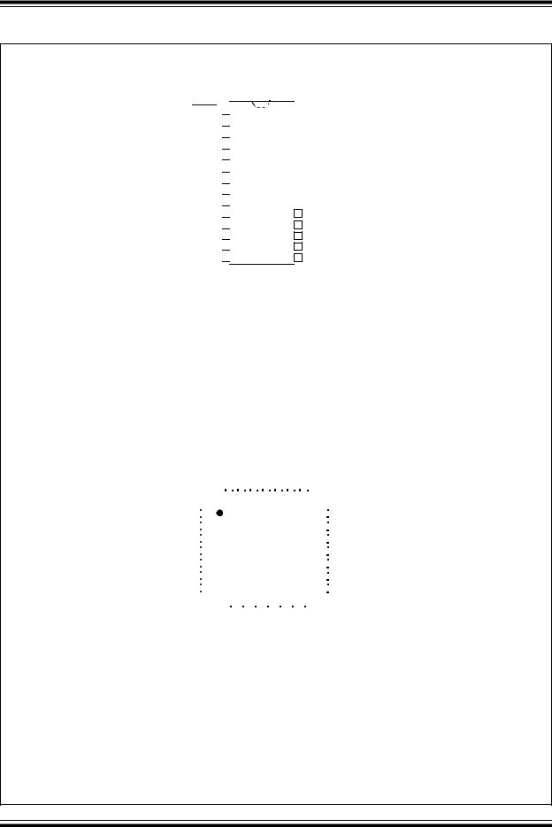
Pin Diagrams
28-PIN SDIP, SOIC
MCLR  1 AN0/VREF+/CN2/RA0
  2 AN1/VREF-/CN3/RA1
  3 PGD1/EMUD1/AN2/C2IN-/RP0/CN4/RB0
  4 PGC1/EMUC1/AN3/C2IN+/RP1/CN5/RB1
  5 AN4/RP2/CN6/RB2
  6 AN5/RP3/CN7/RB3
  7
7
VSS  8 OSCI/CLKI/CN30/RA2
  9
9
OSCO/CLKO/CN29/RA3  10 SOSCI/RP4/CN1/RB4
  11 SOSCO/T1CK/CN0/RA4
  12 VDD
  13
13
PGD3/EMUD3/ASDA1/RP5/CN27/RB5  14
14
dsPIC33FJ32MC202
28 |
|
AVDD |
|
||
27 |
|
AVSS |
|
||
26 |
|
PWM1L1/RP15/CN11/RB15 |
|
||
25 |
|
PWM1H1/RP14/CN12/RB14 |
|
||
24 |
|
PWM1L2/RP13/CN13/RB13 |
|
||
23 |
|
PWM1H2/RP12/CN14/RB12 |
|
||
22 |
|
PGC2/EMUC2/TMS/PWM1L3/RP11/CN15/RB11 |
|
||
21 |
|
PGD2/EMUD2/TDI/PWM1H3/RP10/CN16/RB10 |
|
||
20 |
|
VCAP/VDDCORE |
|
||
19 |
|
VSS |
18 |
|
TDO/PWM2L1/SDA1/RP9/CN21/RB9 |
17 |
|
TCK/PWM2H1/SCL1/RP8/CN22/RB8 |
16 |
|
INT0/RP7/CN23/RB7 |
15 |
|
PGC3/EMUC3/ASCL1/RP6/CN24/RB6 |
|
|
|
28-Pin QFN-S
|
|
AN1/VREF-/CN3/RA1 |
AN0/VREF+/CN2/RA0 |
|
MCLR AVDD |
|
AVSS PWM1L1/RP15/CN11/RB15 |
PWM1H1/RP14/CN12/RB14 |
|
|
|
||||||||||||
|
|
|
|
|
|
|
|||||||||||||||||
|
|
|
|
|
|
|
|
|
|
|
|
|
|
|
|
|
|
|
|
|
|
|
|
|
28 27 26 25 24 23 22 |
|
|
|
|||||||||||||||||||
PGED1/EMUD1/AN2/C2IN-/RP0/CN4/RB0 |
1 |
|
|
|
|
|
|
|
|
|
|
|
|
|
|
|
|
|
|
|
21 |
|
PWM1L2/RP13/CN13/RB13 |
|
|
|
|
|
|
|
|
|
|
|
|
|
|
|
|
|
|
|
|
||||
PGEC1/EMUC1/AN3/C2IN+/RP1/CN5/RB1 |
2 |
|
|
|
|
|
|
|
|
|
|
|
|
|
|
|
|
|
|
|
20 |
|
PWM1H2/RP12/CN14/RB12 |
|
|
|
|
|
|
|
|
|
|
|
|
|
|
|
|
|
|
|
|
||||
AN4/RP2/CN6/RB2 |
3 |
|
|
|
|
|
|
|
|
|
|
|
|
|
|
|
|
|
|
|
19 |
|
PGEC2/EMUC2/TMS/PWM1L3/RP11/CN15/RB11 |
|
|
|
|
|
|
|
|
|
|
|
|
|
|
|
|
|
|
|
|
||||
AN5/RP3/CN7/RB3 |
4 dsPIC33FJ32MC202 |
18 |
|
PGED2/EMUD2/TDI/PWM1H3/RP10/CN16/RB10 |
|||||||||||||||||||
|
|||||||||||||||||||||||
VSS |
5 |
|
|
|
|
|
|
|
|
|
|
|
|
|
|
|
|
|
|
|
17 |
|
VCAP/VDDCORE |
|
|
|
|
|
|
|
|
|
|
|
|
|
|
|
|
|
|
|
|
||||
OSCI/CLKI/CN30/RA2 |
6 |
|
|
|
|
|
|
|
|
|
|
|
|
|
|
|
|
|
|
|
16 |
|
VSS |
|
|
|
|
|
|
|
|
|
|
|
|
|
|
|
|
|
|
|
|
||||
OSCO/CLKO/CN29/RA3 |
7 |
|
|
9 10 11 12 13 14 |
|
15 |
|
TDO/PWM2L1/SDA1/RP9/CN21/RB9 |
|||||||||||||||
|
|
|
|
||||||||||||||||||||
|
8 |
|
|
|
|
|
|||||||||||||||||
|
|
|
|
|
|
|
|
|
|
|
|
|
|
|
|
|
|
|
|
|
|
||
|
SOSCI/RP4/CN1/RB4 |
SOSCO/T1CK/CN0/RA4 VDD PGED3/EMUD3/ASDA1/RP5/CN27/RB5 |
PGEC3/EMUC3/ASCL1/RP6/CN24/RB6 INT0/RP7/CN23/RB7 |
TCK/PWM2H1/SCL1/RP8/CN22/RB8 |
|
|
|
||||||||||||||||
DS70283B-page 4 |
Preliminary |
♥ 2007 Microchip Technology Inc. |

dsPIC33FJ32MC202/204 and dsPIC33FJ16MC304
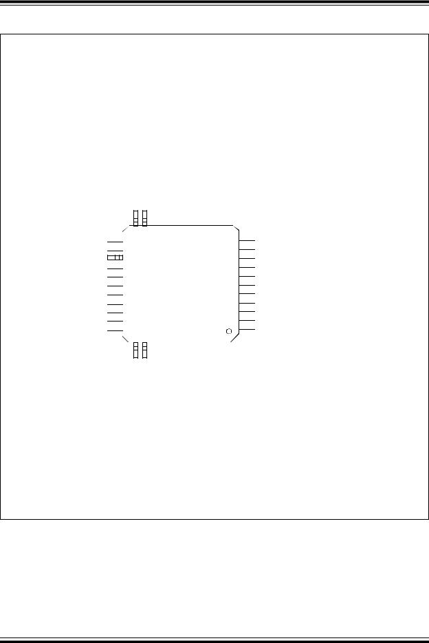
Pin Diagrams (Continued)
44-Pin QFN
|
PGEC1/EMUC1/AN3/C2IN+/RP1/CN5/RB1 |
PGED1/EMUD1/AN2/C2IN-/RP0/CN4/RB0 AN1/VREF-/CN3/RA1 AN0/VREF+/CN2/RA0 |
|
MCLR AVDD AVSS PWM1L1/RP15/CN11/RB15 PWM1H1/RP14/CN12/RB14 TCK/RA7 |
TMS/RA10 |
|
|||||||||||||||||||||||
|
|
|
|||||||||||||||||||||||||||
|
|
|
|
|
|
|
|
|
|
|
|
|
|
|
|
|
|
|
|
|
|
|
|
|
|
|
|
|
|
|
22 21 20 19 18 17 16 15 14 13 12 |
|
|
|
|||||||||||||||||||||||||
AN4/RP2/CN6/RB2 |
23 |
|
|
|
|
|
|
|
|
|
|
|
|
|
|
|
|
|
|
|
|
|
|
|
11 |
|
PWM1L2/RP13/CN13/RB13 |
||
|
|
|
|
|
|
|
|
|
|
|
|
|
|
|
|
|
|
|
|
|
|||||||||
AN5/RP3/CN7/RB3 |
24 |
|
|
|
|
|
|
|
|
|
|
|
|
|
|
|
|
|
|
|
|
|
|
|
10 |
|
PWM1H2/RP12/CN14/RB12 |
||
|
|
|
|
|
|
|
|
|
|
|
|
|
|
|
|
|
|
|
|
|
|||||||||
AN6/RP16/CN8/RC0 |
25 |
|
|
|
|
|
|
|
|
|
|
|
|
|
|
|
|
|
|
|
|
|
|
|
9 |
|
PGEC2/EMUC2/PWM1L3/RP11/CN15/RB11 |
||
|
|
|
|
|
|
|
|
|
|
|
|
|
|
|
|
|
|
|
|
|
|||||||||
AN7/RP17/CN9/RC1 |
26 |
|
|
|
|
|
|
|
|
|
|
|
|
|
|
|
|
|
|
|
|
|
|
|
8 |
|
PGED2/EMUD2/PWM1H3/RP10/CN16/RB10 |
||
|
|
|
|
|
|
|
|
|
|
|
|
|
|
|
|
|
|
|
|
|
|||||||||
AN8/RP18/CN10/RC2 |
27 |
|
|
|
|
|
dsPIC33FJ32MC204 |
7 |
|
VCAP/VDDCORE |
|||||||||||||||||||
|
|
|
|||||||||||||||||||||||||||
VDD |
28 |
|
|
|
|
|
6 |
|
VSS |
||||||||||||||||||||
|
|
|
|
|
dsPIC33FJ16MC304 |
|
|||||||||||||||||||||||
VSS |
29 |
|
|
|
|
|
5 |
|
RP25/CN19/RC9 |
||||||||||||||||||||
|
|
|
|
|
|
|
|
|
|
|
|
|
|
|
|
|
|
|
|
|
|
|
|
||||||
OSCI/CLKI/CN30/RA2 |
30 |
|
|
|
|
|
|
|
|
|
|
|
|
|
|
|
|
|
|
|
|
|
|
|
4 |
|
RP24/CN20/RC8 |
||
|
|
|
|
|
|
|
|
|
|
|
|
|
|
|
|
|
|
|
|
|
|||||||||
OSCO/CLKO/CN29/RA3 |
31 |
|
|
|
|
|
|
|
|
|
|
|
|
|
|
|
|
|
|
|
|
|
|
|
3 |
|
PWM2L1/RP23/CN17/RC7 |
||
|
|
|
|
|
|
|
|
|
|
|
|
|
|
|
|
|
|
|
|
|
|||||||||
TDO/RA8 |
32 |
|
|
|
|
|
|
|
|
|
|
|
|
|
|
|
|
|
|
|
|
|
|
|
2 |
|
PWM2H1/RP22/CN18/RC6 |
||
|
|
|
|
|
|
|
|
|
|
|
|
|
|
|
|
|
|
|
|
|
|||||||||
SOSCI/RP4/CN1/RB4 |
33 |
|
|
|
|
|
|
|
|
|
|
|
|
|
|
|
|
|
|
|
|
|
|
|
1 |
|
SDA1/RP9/CN21/RB9 |
||
|
|
|
|
|
|
|
|
|
|
|
|
|
|
|
|
|
|
|
|
|
|||||||||
|
34 35 36 37 38 39 40 41 42 43 44 |
|
|
|
|||||||||||||||||||||||||
|
|
|
|
|
|
|
|
|
|
|
|
|
|
|
|
|
|
|
|
|
|
|
|
|
|
|
|
|
|
|
SOSCO/T1CK/CN0/RA4 |
TDI/RA9 RP19/CN28/RC3 RP20/CN25/RC4 RP21/CN26/RC5 VSS VDD PGED3/EMUD3/ASDA1/RP5/CN27/RB5 PGEC3/EMUC3/ASCL1/RP6/CN24/RB6 INT0/RP7/CN23/RB7 |
SCL1/RP8/CN22/RB8 |
|
|||||||||||||||||||||||||
♥ 2007 Microchip Technology Inc.
Preliminary
DS70283B-page 5
dsPIC33FJ32MC202/204 and dsPIC33FJ16MC304
Pin Diagrams (Continued)
44-Pin TQFP
AN4/RP2/CN6/RB2
AN5/RP3/CN7/RB3
AN6/RP16/CN8/RC0
AN7/RP17/CN9/RC1
AN8/RP18/CN10/RC2 VDD VSS
OSCI/CLKI/CN30/RA2
OSCO/CLKO/CN29/RA3
TDO/RA8
SOSCI/RP4/CN1/RB4
PGEC1/EMUC1/AN3/C2IN+/RP1/CN5/RB1
22


 23
23 


 24 25
24 25


 26
26


 27
27


 28
28


 29
29


 30
30


 31
31


 32
32  33
33
SOSCO/T1CK/CN0/RA4 34
/RP0/CN4/RB0-PGED1/EMUD1/AN2/C2IN
21
TDI/RA9 35
AN1/VREF-/CN3/RA1 |
AN0/VREF+/CN2/RA0 |
|
AVDD |
AVSS PWM1L1/RP15/CN11/RB15 |
PWM1H1/RP14/CN12/RB14 |
TCK/RA7 TMS/RA10 |
||||||||||||||
MCLR |
||||||||||||||||||||
|
|
|
|
|
|
|
|
|
|
|
|
|
|
|
|
|
|
|
||
|
|
|
|
|
|
|
|
|
|
|
|
|
|
|
|
|
|
|
|
|
|
|
|
|
|
|
|
|
|
|
|
|
|
|
|
|
|
|
|
|
|
|
|
|
|
|
|
|
|
|
|
|
|
|
|
|
|
|
|
|
|
|
20 |
19 |
18 |
17 |
15 16 |
14 |
12 13 |
||||||||||||||
dsPIC33FJ32MC204
dsPIC33FJ16MC304
36 37 |
38 |
39 40 |
41 42 |
43 |
44 |
|||||||||||||
|
|
|
|
|
|
|
|
|
|
|
|
|
|
|
|
|
|
|
|
|
|
|
|
|
|
|
|
|
|
|
|
|
|
|
|
|
|
|
|
|
|
|
|
|
|
|
|
|
|
|
|
|
|
|
|
|
|
|
|
|
|
|
|
|
|
|
|
|
|
|
|
|
|
|
|
RP19/CN28/RC3 RP20/CN25/RC4 |
RP21/CN26/RC5 |
VSS VDD |
PGED3/EMUD3/ASDA1/RP5/CN27/RB5 PGEC3/EMUC3/ASCL1/RP6/CN24/RB6 |
INT0/RP7/CN23/RB7 |
SCL1/RP8/CN22/RB8 |
|||||||||||||
11 
10 
9 
8 
7 
6 
5 
4 
3 
2 
1 
PWM1L2/RP13/CN13/RB13
PWM1H2/RP12/CN14/RB12
PGEC2/EMUC2/PWM1L3/RP11/CN15/RB11
PGED2/EMUD2/PWM1H3/RP10/CN16/RB10 VCAP/VDDCORE
VSS
RP25/CN19/RC9
RP24/CN20/RC8
PWM2L1/RP23/CN17/RC7
PWM2H1/RP22/CN18/RC6
SDA1/RP9/CN21/RB9
DS70283B-page 6 |
Preliminary |
♥ 2007 Microchip Technology Inc. |

dsPIC33FJ32MC202/204 and dsPIC33FJ16MC304
Table of Contents |
|
|
dsPIC33FJ32MC202/204 and dsPIC33FJ16MC304 Product Families.................................................................................................. |
3 |
|
1.0 |
Device Overview .......................................................................................................................................................................... |
9 |
2.0 |
CPU ............................................................................................................................................................................................ |
13 |
3.0 |
Memory Organization ................................................................................................................................................................. |
25 |
4.0 |
Flash Program Memory .............................................................................................................................................................. |
51 |
5.0 |
Resets ....................................................................................................................................................................................... |
57 |
6.0 |
Interrupt Controller ..................................................................................................................................................................... |
63 |
7.0 |
Oscillator Configuration .............................................................................................................................................................. |
95 |
8.0 |
Power - Saving Features ............................................................................................................................................................ |
105 |
9.0 |
I/O Ports ................................................................................................................................................................................... |
107 |
10.0 |
Timer1 ...................................................................................................................................................................................... |
133 |
11.0 |
Timer2/3 feature ...................................................................................................................................................................... |
135 |
12.0 |
Input Capture ............................................................................................................................................................................ |
141 |
13.0 |
Output Compare ....................................................................................................................................................................... |
143 |
14.0 |
Motor Control PWM Module ..................................................................................................................................................... |
147 |
15.0 |
Quadrature Encoder Interface (QEI) Module ........................................................................................................................... |
169 |
16.0 |
Serial Peripheral Interface (SPI) ............................................................................................................................................... |
177 |
17.0 |
Inter - Integrated Circuit (I 2 C) ..................................................................................................................................................... |
185 |
18.0 |
Universal Asynchronous Receiver Transmitter (UART) ........................................................................................................... |
195 |
19.0 |
10 - bit/12 - bit Analog - to - Digital Converter (ADC) ....................................................................................................................... |
203 |
20.0 |
Special Features ...................................................................................................................................................................... |
217 |
21.0 |
Instruction Set Summary .......................................................................................................................................................... |
225 |
22.0 |
Development Support ............................................................................................................................................................... |
233 |
23.0 |
Electrical Characteristics .......................................................................................................................................................... |
237 |
24.0 |
Packaging Information .............................................................................................................................................................. |
275 |
Appendix A: Revision History............................................................................................................................................................. |
281 |
|
Index |
.......................................................................................................................... ....................................................................... |
283 |
The Microchip Web Site..................................................................................................................................................................... |
287 |
|
Customer ..............................................................................................................................................Change Notification Service |
287 |
|
Customer ..............................................................................................................................................................................Support |
287 |
|
Reader ..............................................................................................................................................................................Response |
288 |
|
Product ............................................................................................................................................................Identification System |
289 |
|
TO OUR VALUED CUSTOMERS
It is our intention to provide our valued customers with the best documentation possible to ensure successful use of your Microchip products. To this end, we will continue to improve our publications to better suit your needs. Our publications will be refined and enhanced as new volumes and updates are introduced.
If you have any questions or comments regarding this publication, please contact the Marketing Communications Department via E-mail at docerrors@microchip.com or fax the Reader Response Form in the back of this data sheet to (480) 792-4150. We welcome your feedback.
Most Current Data Sheet
To obtain the most up-to-date version of this data sheet, please register at our Worldwide Web site at: http://www.microchip.com
You can determine the version of a data sheet by examining its literature number found on the bottom outside corner of any page. The last character of the literature number is the version number, (e.g., DS30000A is version A of document DS30000).
Errata
An errata sheet, describing minor operational differences from the data sheet and recommended workarounds, may exist for current devices. As device/documentation issues become known to us, we will publish an errata sheet. The errata will specify the revision of silicon and revision of document to which it applies.
To determine if an errata sheet exists for a particular device, please check with one of the following:
•Microchip’s Worldwide Web site; http://www.microchip.com
•Your local Microchip sales office (see last page)
When contacting a sales office, please specify which device, revision of silicon and data sheet (include literature number) you are using.
Customer Notification System
Register on our web site at www.microchip.com to receive the most current information on all of our products.
♥ 2007 Microchip Technology Inc.
Preliminary
DS70283B-page 7

dsPIC33FJ32MC202/204 and dsPIC33FJ16MC304
NOTES:
DS70283B-page 8 |
Preliminary |
♥ 2007 Microchip Technology Inc. |