

Digital-Logic
.pdfB3 B2
B1 B0 00 01 11 10
00 |
0 |
4 |
x |
8 |
|
01 |
1 |
5 |
|
x |
9 |
11 |
3 |
7 |
|
x |
x |
10 |
2 |
6 |
|
x |
x |
S5 = 0+2+6+8 |
|
|
|||
B3 B2 |
|
S5 |
|
|
|
B1 B0 |
00 |
01 |
11 |
10 |
|
00 |
1 |
0 |
|
x |
1 |
01 |
0 |
0 |
|
x |
0 |
11 |
0 |
0 |
|
x |
x |
10 |
1 |
1 |
|
x |
x |
S5 = |
B2B0 |
+ |
B1B0 |
||
BCD-to-7 segment |
|
|
|
|
|
|
|
||||
|
|
|
|
|
S7 = 2+3+4+5+6+8+9 |
||||||
|
|
|
|
|
B3 B2 |
|
|
S7 |
|
||
|
|
|
|
|
|
|
|
|
|
||
|
|
|
|
|
B1 B0 |
00 |
01 |
11 |
10 |
||
|
|
|
|
|
00 |
0 |
1 |
x |
1 |
||
S6 = 0+4+5+6+8+9 |
01 |
0 |
1 |
x |
1 |
||||||
11 |
1 |
0 |
x |
x |
|||||||
B3 B2 |
|
S6 |
|
||||||||
|
|
10 |
1 |
1 |
x |
x |
|||||
B1 B0 |
00 |
01 |
11 |
10 |
|
|
|
|
|
|
|
00 |
1 |
1 |
x |
1 |
S7 = |
B3 + |
B2B1 |
||||
01 |
0 |
1 |
x |
1 |
|
+ |
B1B2 + |
B1B0 |
|||
11 |
0 |
0 |
|
|
|||||||
x |
x |
|
|
|
|
|
|
||||
10 |
0 |
1 |
x |
x |
|
|
|
|
|
|
|
S6 = B3 + |
B1B0 + |
B1B2 + |
B2B0 |
|
|
|
|||||
© Emil M. Petriu
 MEMORY ELEMENTS: LATCHES AND FLIP-FLOPS
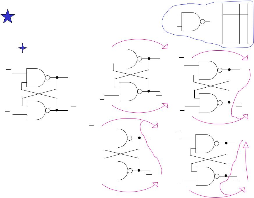
R-S Latch |
|
|
|
|
|
S = 0 |
|
||||
(Reset-Set) |
|
||||
|
|
|
|
|
|
|
|
|
|
|
|
|
|
|
|
|
|
S
Q
|
R = 0 |
R |
Q |
|
|
|
|
|
|
|
|
|
|
S = 1 |
|
|
|
||||
|
|
|
|
|
|
|
|
|
|
|
|
|||||
S R |
Q |
|
|
|
|
|
|
|
|
|
|
|
||||
Q |
|
|
|
|
|
|
|
|
|
|||||||
|
|
|
|
|
|
|
|
|
|
|||||||
|
|
|
|
|
|
|
|
|
|
|
|
|
|
|||
0 |
0 |
|
1 |
1 |
Weird state |
|
|
|
|
|
|
|
|
|||
|
|
|
|
|
|
|
|
|
||||||||
|
|
|
|
|
|
|
|
|
||||||||
0 |
1 |
|
1 |
0 |
Set state |
|
|
|
|
|
|
|
|
|||
|
|
|
|
|
|
|
|
|
||||||||
1 |
0 |
|
0 |
1 |
Reset state |
|
|
|
|
|
|
|
|
|||
1 |
1 |
|
Q |
Q |
Hold state |
|
|
|
|
|
|
|
|
|||
|
R = 0 |
|
|
|
||||||||||||
|
|
|
|
|||||||||||||
|
|
|
|
|
|
|
|
|
|
|
|
|||||
|
|
I1 I2 |
F |
|
I1 |
F |
0 |
0 |
1 |
|
|
|||
I2 |
|
0 |
1 |
1 |
|
|
1 |
0 |
1 |
|
|
1 |
1 |
0 |
Q = 1
S = 0 |
Q = 1 |
Q = 1 |
|
|
|
|
R = 1 |
Q = |
0 |
|
|
|
|
Q = 0 |
S = 1 |
Q = 1 |
|
|
|
Q = 1 |
Q = 0 |
|
R = 1 |
||
|
© Emil M. Petriu
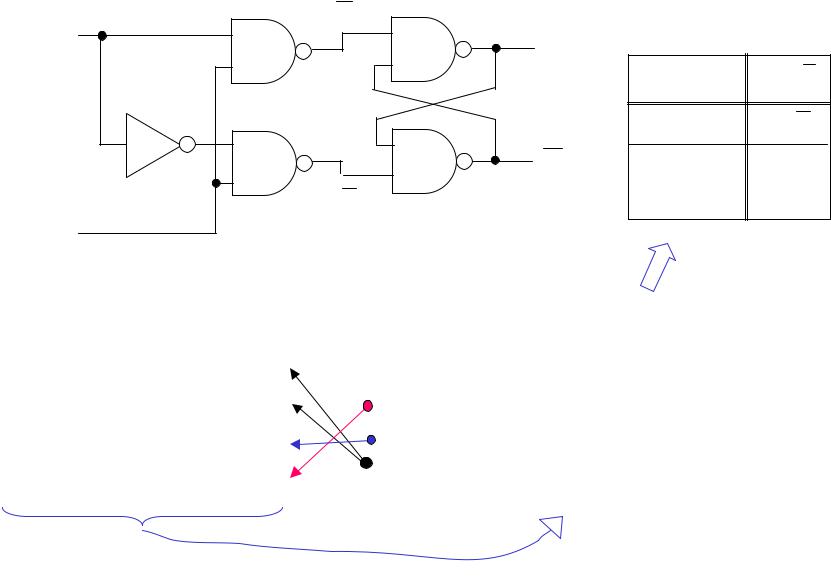
 D (Transparent) Latch
D |
Enable
S |
|
|
|
|
Q |
|
|
|
|
|
Enable D |
Q |
Q |
|
|
0 |
x |
Q |
Q |
Q |
1 |
0 |
0 |
1 |
R |
1 |
1 |
1 |
0 |
|
|
|
|
|
|
|
|
|
|
|
|
|
|
Enable D |
|
S |
R |
Q |
Q |
||||||||
|
|
|
|
|
|
|
|
|
|
|
|
|
|
|
|
|
|
|
|
|
|
|
|
|
|
|
|
0 |
0 |
1 |
1 |
|
Q |
|
|
|
|
|
|||
Q |
|||||||||||||
0 |
1 |
1 |
1 |
|
Q |
|
|
|
|
|
|||
|
Q |
||||||||||||
|
|
|
|
|
|
|
|
|
|
|
|
|
|
1 |
0 |
1 |
0 |
0 |
1 |
|
|||||||
1 |
1 |
0 |
1 |
1 |
0 |
||||||||
|
|
|
|
|
|
|
|
|
|
|
|
|
|
|
|
|
|
|
|
|
|
|
|
|
|
|
|
|
|
|
|
|
|
|
|
S R |
Q Q |
|||||||||
|
|
|
|
|
|
|
|
|
|
|
0 |
0 |
|
1 |
1 |
|
|
||||
0 |
1 |
|
1 |
0 |
|
|
||||
1 |
0 |
|
0 |
1 |
|
|
||||
1 |
1 |
|
Q |
|
Q |
|
|
|||
|
|
|
|
|
|
|
|
|
|
|
When the Enable input
is =1 (i.e. TRUE or HIGH) the information present at the D input is stored in the
latch and will “appear as it is” at the Q output ( => it is like that there is a “transparent” path from the D input to the Q output)
© Emil M. Petriu
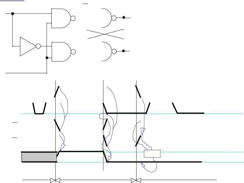
 D Latch
D |
Enable
|
|
S |
|
|
|
|
|
|
|
|
|
|
|
|
|
|
|
|
|
|
|
|
|
|
|
|
|||
|
|
|
|
|
|
|
|
|
|
|
|
Enable D |
|
|
|
|
|
|
|
|
|
|
|
|
|||||
|
|
|
|
|
|
|
|
|
|
|
|
|
Q |
|
|
S |
|
R |
|
Q |
|
|
Q |
|
|||||
|
|
|
|
|
|
|
|
|
|
|
|
|
|||||||||||||||||
|
|
|
|
|
|
|
|
|
|
|
|
|
|||||||||||||||||
|
|
|
|
|
|
|
|
|
|
|
|
|
|
|
|
|
|
|
|
|
|
|
|
|
|
|
|
|
|
|
|
|
|
|
|
|
|
|
|
|
|
|
|
|
|
0 |
0 |
|
1 |
1 |
|
Q |
|
|
|
|
|
||
|
|
|
|
|
|
|
|
|
|
|
|
|
|
|
|
|
|
|
Q |
|
|||||||||
|
|
|
|
|
|
|
|
|
|
|
|
|
|
|
|||||||||||||||
|
|
|
|
|
|
|
|
|
|
|
|
|
|
|
|||||||||||||||
|
|
|
|
|
|
|
|
|
|
|
|
|
|
|
|
0 |
1 |
|
1 |
1 |
|
Q |
|
|
|
|
|||
|
|
|
|
|
|
|
|
|
|
|
|
|
|
|
|
|
|
|
Q |
||||||||||
|
|
|
|
|
|
|
|
|
|
|
|
|
|
|
|||||||||||||||
|
|
|
|
|
|
|
|
|
|
|
|
|
|
|
|||||||||||||||
|
|
|
|
|
|
|
|
|
|
|
|
|
|
|
|
|
|
|
|
|
|
|
|
|
|
|
|
|
|
|
|
|
|
|
|
|
|
|
|
|
|
|
|
Q |
|
1 |
0 |
|
1 |
0 |
0 |
1 |
|||||||
|
|
|
|
|
|
|
|
|
|
|
|
|
|||||||||||||||||
|
|
|
|
|
|
|
|
|
|
|
|
|
|
||||||||||||||||
|
|
|
|
|
|
|
|
|
|
|
|
1 |
1 |
|
0 |
1 |
1 |
0 |
|||||||||||
R |
|
|
|
|
|
|
|
||||||||||||||||||||||
|
|||||||||||||||||||||||||||||
|
|
|
|
|
|
|
|
|
|
|
|
|
|
|
|
|
|
|
|
|
|
|
|
|
|
|
|
|
|
 1
1
Enable

 0
0  1
1
D |
0 |
|
 1
1
S  0
0
 1
1
R  0
0
Q |
Hold |
1 |
|
||
|
0 |
|
|
|
“Hold”state |
“Transparent” state |
“Hold”state |
© Emil M. Petriu
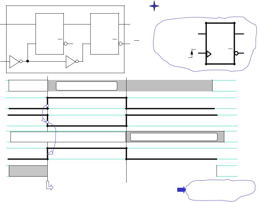
|
Latch 1 |
Latch 2 |
|
|
Synchronous D Flip-Flop |
||||
|
|
|
|
|
|
|
|||
D |
D |
Q |
D1 |
Q |
Q |
|
|
|
|
D |
Positive-Edge |
|
|
||||||
|
|
|
|
|
|
D |
Q |
||
|
|
|
|
|
|
-Triggered |
|
||
|
Enab. |
Q |
Enab. |
Q |
Q |
|
|
|
|
|
D Flip-Flop |
|
CLK |
|
|||||
|
|
|
|
|
|
|
|
Q |
|
|
|
|
|
|
|
|
|
|
|
CLK |
EN1 |
|
EN2 |
|
|
|
|
|
|
|
|
|
|
|
|
|
|
||
D |
Din* |
Input data D may change |
|
|
|
|
1 |
||
|
|
|
|
0 |
|||||
|
|
|
|
|
|
|
|
|
|
CLK |
|
|
|
|
|
|
|
|
1 |
|
|
|
|
|
|
|
|
0 |
|
|
|
|
|
|
|
|
|
|
|
EN1 |
Latch 1 is |
|
Latch 1 is Holding |
|
|
Latch 1 is Transparent |
|
1 |
|
|
|
|
|
0 |
|||||
|
Transparent |
|
|
|
|
|
|
|
|
D1 |
D1 = Din* |
|
|
|
Changed input data D enter Latch 1 |
1 |
|||
|
|
|
0 |
||||||
|
|
|
|
|
|
|
|
|
|
EN2 Latch 2 is Holding |
|
Latch 2 is Transparent |
|
Latch 2 is Holding |
|
|
1 |
||
|
|
|
|
0 |
|||||
|
|
|
|
|
|
|
|
|
|
Q |
|
|
Q = D1 = Din* |
|
|
|
|
|
1 |
|
|
|
|
|
|
|
0 |
||
|
|
|
|
|
|
|
|
|
|
|
|
The state of the flip-flop’s output Q copies input |
Positive-Edge-Triggered |
||||||
|
|
D when the positive edge of the clock CLK occurs |
D Flip-Flop |
|
|||||
|
|
|
|
|
|
|
|
||
© Emil M. Petriu
 Synchronous D Flip-Flop
Vcc CLR2 |
D2 |
CLK2 |
PR2 |
Q2 |
Q2 |
||
14 |
13 |
|
12 |
11 |
10 |
9 |
8 |
1 |
2 |
|
3 |
4 |
5 |
6 |
7 |
CLR1 |
D1 |
CLK1 |
PR1 |
Q1 |
Q1 |
GND |
|
Connection diagram of the 7474 Dual
Positive-Edge-Triggered D Flip-Flops with Preset and Clear.
© Emil M. Petriu
 COUNTERS
 4-Bit Synchronous Counter using D Flip-Flops
Q3 |
Q2 |
Q1 |
Q0 |
0 |
1 |
2 |
3 |
4 |
5 |
|
|
|
|
||||||
|
|
|
|
15 |
CL |
|
|
|
6 |
4-Bit BINARY COUNTER |
|
|
|
|
|||||
|
|
|
|
14 |
|
|
|
|
7 |
CK |
|
|
CL |
|
|
|
|
|
|
|
|
|
|
|
|
|
|
||
|
3 |
|
2i |
13 |
12 |
11 |
10 |
9 |
8 |
Q = Σ Qi . |
|
|
|
|
|
|
|||
i = 0
CK |
|
|
|
|
|
|
|
|
|
|
|
|
|
|
|
|
CL |
|
|
|
|
|
|
|
|
|
|
|
|
|
|
|
|
Q |
0 |
1 |
2 |
3 |
4 |
5 |
6 |
7 |
8 |
9 10 11 12 13 14 15 0 |
1 |
2 |
3 |
4 |
5 |
6 |
1
0
1
0
© Emil M. Petriu
DECIMAL |
|
BINARY STATE OF |
FLIP FLOP INPUTS |
||||||
|
|||||||||
STATE |
|
THE COUNTER |
(for the next state) |
||||||
|
|
|
|
|
|
|
|
|
|
Q |
|
Q3 |
Q2 |
Q1 |
Q0 |
D3 |
D2 |
D1 D0 |
|
|
|
|
|
|
|
|
|
|
|
|
|
|
|
|
|
|
|
|
|
0 |
|
0 |
0 |
0 |
0 |
0 |
0 |
0 |
1 |
1 |
|
0 |
0 |
0 |
1 |
0 |
0 |
1 |
0 |
2 |
|
0 |
0 |
1 |
0 |
0 |
0 |
1 |
1 |
3 |
|
0 |
0 |
1 |
1 |
0 |
1 |
0 |
0 |
4 |
|
0 |
1 |
0 |
0 |
0 |
1 |
0 |
1 |
5 |
|
0 |
1 |
0 |
1 |
0 |
1 |
1 |
0 |
6 |
|
0 |
1 |
1 |
0 |
0 |
1 |
1 |
1 |
7 |
|
0 |
1 |
1 |
1 |
1 |
0 |
0 |
0 |
8 |
|
1 |
0 |
0 |
0 |
1 |
0 |
0 |
1 |
9 |
|
1 |
0 |
0 |
1 |
1 |
0 |
1 |
0 |
10 |
|
1 |
0 |
1 |
0 |
1 |
0 |
1 |
1 |
11 |
|
1 |
0 |
1 |
1 |
1 |
1 |
0 |
0 |
12 |
|
1 |
1 |
0 |
0 |
1 |
1 |
0 |
1 |
13 |
|
1 |
1 |
0 |
1 |
1 |
1 |
1 |
0 |
14 |
|
1 |
1 |
1 |
0 |
1 |
1 |
1 |
1 |
15 |
|
1 |
1 |
1 |
1 |
0 |
0 |
0 |
0 |
0 |
|
0 |
0 |
0 |
0 |
|
|
|
|
|
|
|
|
|
|
|
|
|
|
|
|
|
|
|
|
|
|
|
|
 Synchronous 4-bit Counter
Using D flip-flops has the distinct advantage of a straightforward definition of the flip-flop inputs: the current state of these inputs is the next state of the counter. The logic equations for all four flip-flop inputs D3, D2,
D1, and D0 are derived from this truth table as
functions of the
current states of the counter’s flip-flops:
Q3, Q2, Q1, and Q0. Karnaugh maps can be used to simplify these equations.
Q3 Q2 |
|
|
D3 |
|
|
Q3 Q2 |
|
|
D2 |
|
|
|
Q3 Q2 |
|
D1 |
|
|
|
Q3 Q2 |
|
D0 |
|
||||
|
|
|
|
|
|
|
|
|
|
|
|
|||||||||||||||
Q1 Q0 |
|
00 |
01 |
11 |
10 |
|
Q1 Q0 |
|
00 |
01 |
11 |
10 |
|
Q1 Q0 |
00 |
01 |
11 |
10 |
|
Q1 Q0 |
00 |
01 |
11 |
10 |
||
00 |
|
0 |
0 |
1 |
1 |
|
00 |
|
0 |
1 |
1 |
0 |
|
00 |
0 |
0 |
0 |
0 |
|
00 |
1 |
1 |
1 |
1 |
||
|
|
|
|
|
|
|
|
|
|
|
|
|
|
|
|
1 |
1 |
1 |
1 |
|
|
|
0 |
0 |
0 |
0 |
01 |
|
0 |
0 |
1 |
1 |
|
01 |
|
0 |
1 |
1 |
0 |
01 |
01 |
||||||||||||
11 |
|
0 |
1 |
0 |
1 |
|
11 |
|
1 |
0 |
0 |
1 |
|
11 |
0 |
0 |
0 |
0 |
|
11 |
0 |
0 |
0 |
0 |
||
10 |
|
0 |
0 |
1 |
1 |
|
10 |
|
0 |
1 |
1 |
0 |
10 |
1 |
1 |
1 |
1 |
10 |
1 |
1 |
1 |
1 |
||||
|
|
|
|
|
|
|
|
|
|
|
|
|
|
|
|
|
|
|
|
|
|
|
|
|
|
|
© Emil M. Petriu
 Synchronous 4-bit Counter
Q3 Q2 |
|
D3 |
|
|
|
|
||
Q1 Q0 |
00 |
01 |
|
11 |
10 |
|
|
|
|
|
|
|
|
|
|
|
|
|
|
|
|
|
|
|
|
|
00 |
0 |
0 |
|
1 |
|
1 |
|
|
01 |
0 |
0 |
|
1 |
|
1 |
|
|
11 |
0 |
1 |
|
0 |
|
1 |
|
|
10 |
0 |
0 |
|
1 |
|
1 |
|
|
|
|
|
|
|
|
|
|
|
|
|
|
|
|
|
|
|
|
D3 = Q3. Q2 + Q3. Q1 + Q3.Q0 + Q3.Q2.Q1.Q0
Q3 Q2 |
|
|
D1 |
|
|
|
|
|
|
|
|
|
Q1 Q0 |
00 |
01 |
11 |
10 |
|
|
|
|
|
|
|
|
|
|
|
|
|
|
|
|
|
|
|
|
|
|
|
|
|
|
|
|
|
|
|
|
|
|
00 |
0 |
0 |
0 |
0 |
|
|
D1 = Q1. Q0 + Q1. Q0 |
|||||
|
|
|
|
|
|
|
|
|
|
|
|
|
01 |
|
1 |
1 |
1 |
1 |
|
|
|
|
|
|
|
11 |
|
|
|
|
|
|
|
|
|
|
|
|
0 |
0 |
0 |
0 |
|
|
|
|
|
|
|
||
|
|
|
|
|
|
|
|
|
|
|
|
|
|
|
|
|
|
|
|
|
|
|
|
|
|
10 |
|
1 |
1 |
1 |
1 |
|
|
|
|
|
|
|
|
|
|
|
|
|
|
|
|
|
|
|
|
Q3 Q2 |
|
|
D2 |
|
||
Q1 Q0 |
00 |
01 |
11 |
|
10 |
|
|
|
|
|
|
|
|
|
|
|
|
|
|
|
|
0 |
|
|
|
|
0 |
00 |
|
1 |
1 |
|
||
01 |
0 |
|
1 |
1 |
|
0 |
11 |
|
|
|
|
|
|
1 |
0 |
0 |
|
1 |
||
|
|
|
|
|
|
|
10 |
0 |
1 |
1 |
|
0 |
|
|
|
|
|
|
|
|
D2 = Q2. Q0 + Q2. Q1 + Q2. Q1. Q0
Q3 Q2 |
|
D0 |
|
|
|
|
||
Q1 Q0 |
00 |
01 |
11 |
10 |
|
|
|
|
|
|
|
|
|
|
|
||
|
|
|
|
|
D0 = Q0 |
|||
00 |
1 |
1 |
1 |
1 |
||||
|
|
|
||||||
01 |
0 |
0 |
0 |
0 |
|
|
|
|
11 |
|
|
|
|
|
|
|
|
0 |
0 |
0 |
0 |
|
|
|
||
|
|
|
|
|
|
|
|
|
10 |
1 |
1 |
1 |
1 |
|
|
|
|
|
|
|
|
|
|
|
|
|
© Emil M. Petriu
 Synchronous 4-bit Counter
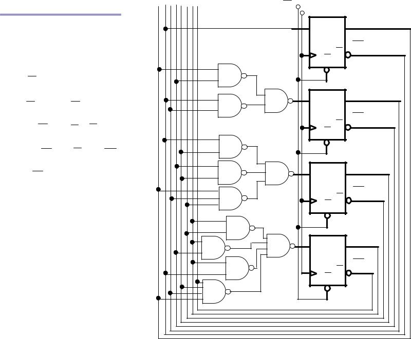
D0 = Q0
D1 = Q1. Q0 + Q1. Q0
D2 = Q2. Q0 + Q2. Q1 + Q2. Q1. Q0
D3 = Q3. Q2 + Q3. Q1 + Q3.Q0
+ Q3.Q2.Q1.Q0
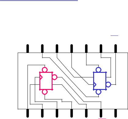
CL |
CK |
|
|
|
Q0 |
|
D |
Q |
|
CLK |
Q0 |
|
R |
Q |
|
|
|
|
|
Q1 |
|
D |
Q |
|
CLK |
Q1 |
|
R |
Q |
|
|
|
|
|
Q2 |
|
D |
Q |
|
CLK |
Q2 |
|
R |
Q |
|
|
|
|
|
Q3 |
|
D |
Q |
|
CLK |
Q3 |
|
R |
Q |
|
|
© Emil M. Petriu