

Bologna / 01_TCAD_laboratory_Introduction_GBB_20150225
.pdfTechnology Computer Aided
Design (TCAD) Laboratory
Lecture 1, Introduction
[Source: Synopsys]
Giovanni Betti Beneventi
E-mail: giovanni.betti2@unibo.it ; giobettibeneventi@gmail.com
Office: School of Engineering, ARCES Lab. (room Ex. 3.2), viale del Risorgimento 2, Bologna
Phone: +39-051-209-3773
Advanced Research Center on Electronic Systems (ARCES)
University of Bologna, Italy
G. Betti Beneventi |
1 |

About the course |
1/2 |
•The main part of the course will be devoted to the practical use of a commercial TCAD software. The activities will be held in the ARCES Lab (room Ex. 3.2).
•The two fundamental questions What is TCAD? Why TCAD? will be answered in this lecture.
•Some theoretical background will be introduced as well to provide a mathematical and physical foundation to support the TCAD activities. The theoretical lessons will be delivered by Prof. M. Rudan.
•The exam consists in two tests:
–A TCAD design project strictly related to the content of the course. The project will be carried out by the students during the last week of the course, directly during the course class, in the ARCES Lab (room Ex. 3.2).
–A questionnaire about the theoretical background part
–No mark will be given, the outcome will be either ‘passed’ or ‘not passed’
G. Betti Beneventi |
2 |
About the course |
2/2 |
|
|
• Course notes can be downloaded from following website
www.micro.deis.unibo.it/~rudan/MATERIALE_DIDATTICO/di apositive/TCAD/diapo_TCAD_index.html
•The days before the class, please check the page “Notices” (“Avvisi”, in the Italian version) of my UniBo website for possible last minute communications (rescheduled lessons, change of agenda, etc.), see
people.unibo.it/it/giovanni.betti2
G. Betti Beneventi |
3 |

Outline
•Physical Modeling
•What is TCAD?
•Why TCAD?
•A link to the context
•In this class
•To probe further
G. Betti Beneventi |
4 |

Outline
Physical Modeling
•What is TCAD?
•Why TCAD?
•A link to the context
•In this class
•To probe further
G. Betti Beneventi |
5 |

Physical modeling: definitions
Physical Modeling
Representation of the physical behavior of a system (device) by an abstract mathematical model which approximates this behavior. Such a model may either be a closed-form expression (analytical model), or, in general, a system of coupled (differential) equations to be solved numerically.
Analytical Modeling vs. Numerical Modeling
Analytical modeling basically means the representation of a physical property or law in terms of approximate closed-form expressions using “lumped” parameters. It is also called “compact” modeling.
Numerical modeling: modeling of the device behavior through the numerical solution of the differential equations describing the device physics on a given geometrical domain.
Note: In the literature, the word “modeling” usually implies analytical/compact modeling, while “simulation” is much used for numerical modeling.
G. Betti Beneventi |
6 |
Examples
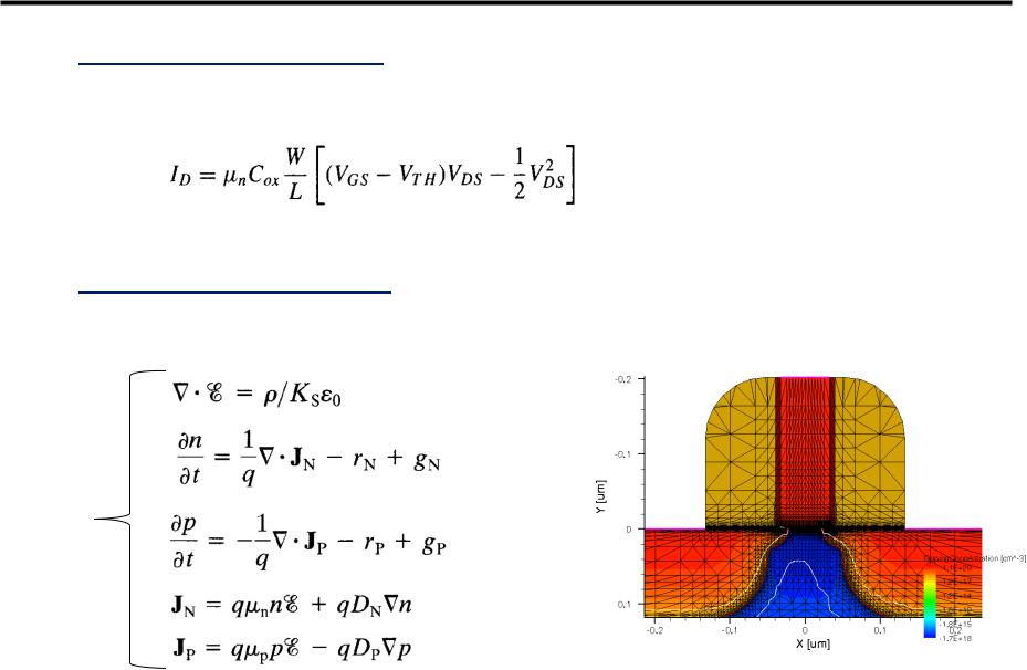
•Analytical modeling
–IDS-VDS curve of a MOS transistor
•Numerical modeling
–Drift-Diffusion numerical model
solved at each node of a discretized domain
G. Betti Beneventi |
7 |

Physical modeling: Pros & Cons
•Analytical Modeling
Captures the essential concepts of device physics.
Very effective to single out the most important aspects of a problem. Computationally efficient. Statistical analysis can be afforded.
Limited applicability: hard to describe problems with complex geometry or very rich physics (e.g., “multiphysical” problem, i.e. coupled equations).
New, physical models need significant a-priori understanding of the problem and long developing times.
•Numerical Modeling
Allows for the description of more complex phenomena (physics & geometry).
Addresses also problems that do not have a closed-form solution.
More flexible, does not always need a depth a-priori understanding of the problem. More reliable from a quantitative point of view.
High computational burden. Statistical analysis hard to be afforded.
More difficult framework to interpret the results and to single out essential points. Require complex software architectures or expensive licenses of commercial tools.
G. Betti Beneventi |
8 |

Physical modeling of semiconductor devices
•Analytical and numerical modeling are complementary techniques, that are often used together in both industry and academia, with different specific aims. In the semiconductor device field, compact models and numerical simulation are expected to interact with each other in the semiconductor chip design flow (see next).
•Nowadays, in the semiconductor industry compact models are mainly used for circuit-device interaction (circuit simulators), statistical analysis and on- the-fly screening of experimental results.
•Numerical simulation is much used to understand advanced device physics, for device design, scaling analyses & interaction with process manufacturing.
•Of course, any kind of modeling should always be validated (or, in some cases, calibrated) with respect to the available experimental data.
•This course will be about numerical modeling of semiconductor devices, usually named as TCAD, which stands for “Technology Computer-Aided Design” (see next).
G. Betti Beneventi |
9 |

Outline
•Physical Modeling
What is TCAD?
•Why TCAD?
•A link to the context
•In this class
•To probe further
G. Betti Beneventi 10