Для магистратуры / lect0
.pdf
Lecture 0:
Introduction

Introduction
Integrated circuits: many transistors on one chip.
Very Large Scale Integration (VLSI): bucketloads!
Complementary Metal Oxide Semiconductor
–Fast, cheap, low power transistors
Today: How to build your own simple CMOS chip
–CMOS transistors
–Building logic gates from transistors
–Transistor layout and fabrication
Rest of the course: How to build a good CMOS chip
0: Introduction |
CMOS VLSI Design 4th Ed. |
2 |

Silicon Lattice
Transistors are built on a silicon substrate
Silicon is a Group IV material
Forms crystal lattice with bonds to four neighbors
 Si
Si  Si
Si  Si
Si 
 Si
Si  Si
Si  Si
Si 
 Si
Si  Si
Si  Si
Si 
0: Introduction |
CMOS VLSI Design 4th Ed. |
3 |

Dopants
Silicon is a semiconductor
Pure silicon has no free carriers and conducts poorly
Adding dopants increases the conductivity
Group V: extra electron (n-type)
Group III: missing electron, called hole (p-type)
Si |
|
Si- |
|
|
Si |
|
|
|
Si |
|
Si+ |
|
Si |
||||||||||||
|
|
|
|
|
|
||||||||||||||||||||
|
|
|
|
|
|
|
|
||||||||||||||||||
|
|
|
|
|
|
|
|
|
|
|
|
|
|
|
|||||||||||
|
|
|
|
As+ |
|
|
|
|
|
|
|
|
|
|
|
|
B- |
|
|
|
|
||||
Si |
Si |
|
|
|
Si |
Si |
|||||||||||||||||||
|
|
|
|
|
|
|
|||||||||||||||||||
|
|
|
|
|
|
|
|
||||||||||||||||||
|
|
|
|
|
|
|
|
|
|
|
|
|
|
|
|
|
|
|
|
|
|
|
|
|
|
Si |
|
Si |
|
|
Si |
|
|
|
Si |
|
Si |
|
Si |
||||||||||||
|
|
|
|
|
|
|
|||||||||||||||||||
|
|
|
|
|
|
|
|
||||||||||||||||||
0: Introduction |
CMOS VLSI Design 4th Ed. |
4 |

p-n Junctions
A junction between p-type and n-type semiconductor forms a diode.
Current flows only in one direction
p-type  n-type
anode cathode
0: Introduction |
CMOS VLSI Design 4th Ed. |
5 |

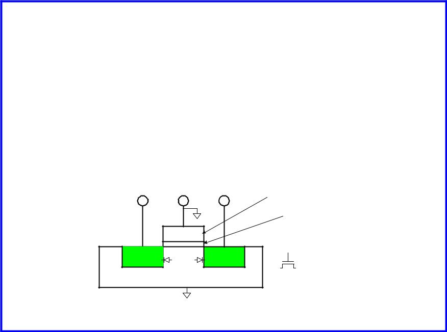
nMOS Transistor
Four terminals: gate, source, drain, body
Gate – oxide – body stack looks like a capacitor
–Gate and body are conductors
–SiO2 (oxide) is a very good insulator
–Called metal – oxide – semiconductor (MOS) capacitor
– Even though gate is
no longer made of metal |
0: Introduction |
CMOS VLSI Design 4th Ed. |
6 |

nMOS Operation
Body is usually tied to ground (0 V)
When the gate is at a low voltage:
–P-type body is at low voltage
–Source-body and drain-body diodes are OFF
–No current flows, transistor is OFF
Source |
Gate |
Drain |
|
|
|
Polysilicon |
|
|
|
|
SiO2 |
n+ |
|
n+ |
0 |
|
|
||
|
p |
S |
D |
|
bulk Si |
|
|
0: Introduction |
CMOS VLSI Design 4th Ed. |
7 |

nMOS Operation Cont.
When the gate is at a high voltage:
–Positive charge on gate of MOS capacitor
–Negative charge attracted to body
–Inverts a channel under gate to n-type
–Now current can flow through n-type silicon from
source through channel to drain, transistor is ON
Source |
Gate |
Drain |
|
|
|
Polysilicon |
|
|
|
|
SiO2 |
n+ |
|
n+ |
1 |
|
|
||
|
p |
S |
D |
|
bulk Si |
|
|
0: Introduction |
CMOS VLSI Design 4th Ed. |
8 |

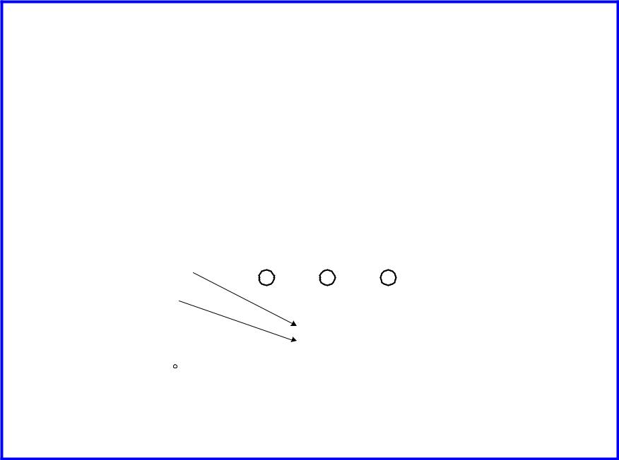
pMOS Transistor
Similar, but doping and voltages reversed
–Body tied to high voltage (VDD)
–Gate low: transistor ON
–Gate high: transistor OFF
–Bubble indicates inverted behavior
|
|
|
|
|
|
|
|
|
|
|
|
|
|
|
|
|
|
|
|
|
|
|
|
|
|
|
|
|
|
|
|
|
|
|
|
|
|
|
|
|
|
|
|
|
|
|
|
|
|
|
|
|
|
|
|
|
|
|
|
|
|
|
|
|
|
|
|
|
|
|
|
|
|
|
|
|
|
|
|
|
|
|
|
|
|
|
|
|
|
|
|
|
|
|
|
|
|
|
|
|
|
|
|
|
|
|
|
|
|
|
|
|
|
|
|
|
|
|
|
|
|
|
|
|
|
|
|
|
|
|
|
|
|
|
0: Introduction |
CMOS VLSI Design 4th Ed. |
9 |
||||||||||||

Power Supply Voltage
GND = 0 V
In 1980’s, VDD = 5V
VDD has decreased in modern processes
–High VDD would damage modern tiny transistors
–Lower VDD saves power
VDD = 3.3, 2.5, 1.8, 1.5, 1.2, 1.0, …
0: Introduction |
CMOS VLSI Design 4th Ed. |
10 |
