

Lab2 / Литература / Описания датчиков / DS18B20 Programmable Resolution 1-Wire Digital Thermometer
.PDFwww.maxim-ic.com
FEATURES
Unique 1-Wire® interface requires only one port pin for communication
Each device has a unique 64-bit serial code stored in an onboard ROM
Multidrop capability simplifies distributed temperature sensing applications
Requires no external components
Can be powered from data line. Power supply range is 3.0V to 5.5V
Measures temperatures from –55°C to +125°C (–67°F to +257°F)
0.5 C accuracy from –10°C to +85°C
Thermometer resolution is user-selectable from 9 to 12 bits
Converts temperature to 12-bit digital word in 750ms (max.)
User-definable nonvolatile (NV) alarm settings
Alarm search command identifies and addresses devices whose temperature is outside of programmed limits (temperature alarm condition)
Available in 8-pin SO (150mil), 8-pin SOP, and 3-pin TO-92 packages
Software compatible with the DS1822
Applications include thermostatic controls, industrial systems, consumer products, thermometers, or any thermally sensitive system
DS18B20
Programmable Resolution
1-Wire Digital Thermometer
PIN ASSIGNMENT
DALLAS |
NC |
|
|
|
|
|
|
NC |
||
|
1 |
|
|
8 |
|
|||||
|
|
|
|
|||||||
18B20 |
|
NC |
|
2 |
18B20 |
DALLAS |
7 |
|
NC |
|
1 |
2 |
3 |
|
|
||||||
|
|
|
|
|||||||
VDD |
|
3 |
|
|
6 |
|
NC |
|||
|
|
|
|
|
|
|
||||
|
|
|
|
|
|
|
||||
|
|
|
DQ |
|
4 |
|
|
5 |
|
GND |
|
|
|
|
|
|
|
||||
|
|
|
|
|
|
|
|
|
|
|
8-Pin 150mil SO
(DS18B20Z)
|
|
|
|
|
|
|
|
|
|
DQ |
|
|
|
|
|
VDD |
|
GND |
DQ V |
|
1 |
18B20 |
8 |
|
|||||||||
|
|
|
||||||||||||||
|
|
|
||||||||||||||
|
NC |
|
3 |
6 |
|
NC |
||||||||||
|
|
|
|
|
|
|
DD |
NC |
|
2 |
|
7 |
|
NC |
||
|
|
|
|
|
|
|
|
|
|
|
|
|
||||
|
|
|
|
|
|
|
|
|
|
GND |
|
4 |
|
5 |
|
NC |
1 |
2 |
3 |
|
|
|
|
|
|||||||||
|
|
|
|
|
||||||||||||
|
|
|
|
|
||||||||||||
|
|
|
8-Pin SOP |
|
||||||||||||
|
|
|
|
|
|
|
|
|
|
|
|
|||||
(BOTTOM VIEW) |
|
(DS18B20U) |
|
|||||||||||||
TO-92 (DS18B20)
PIN DESCRIPTION
GND |
- Ground |
DQ |
- Data In/Out |
VDD |
- Power Supply Voltage |
NC |
- No Connect |
DESCRIPTION
The DS18B20 Digital Thermometer provides 9 to 12–bit centigrade temperature measurements and has an alarm function with nonvolatile user-programmable upper and lower trigger points. The DS18B20 communicates over a 1-Wire bus that by definition requires only one data line (and ground) for communication with a central microprocessor. It has an operating temperature range of –55°C to +125°C and is accurate to 0.5 C over the range of –10°C to +85°C. In addition, the DS18B20 can derive power directly from the data line (“parasite power”), eliminating the need for an external power supply.
Each DS18B20 has a unique 64-bit serial code, which allows multiple DS18B20s to function on the same 1–wire bus; thus, it is simple to use one microprocessor to control many DS18B20s distributed over a large area. Applications that can benefit from this feature include HVAC environmental controls, temperature monitoring systems inside buildings, equipment or machinery, and process monitoring and control systems.
1-Wire is a registered trademark of Dallas Semiconductor. |
1 of 20 |
050102 |
DS18B20
DETAILED PIN DESCRIPTIONS Table 1
SO* SOP* TO-92 SYMBOL DESCRIPTION
5 |
4 |
1 |
GND |
Ground. |
4 |
1 |
2 |
DQ |
Data Input/Output pin. Open-drain 1-Wire interface pin. |
|
|
|
|
Also provides power to the device when used in parasite |
|
|
|
|
power mode (see “Parasite Power” section.) |
3 |
8 |
3 |
VDD |
Optional VDD pin. VDD must be grounded for operation in |
|
|
|
|
parasite power mode. |
*All pins not specified in this table are “No Connect” pins.
OVERVIEW
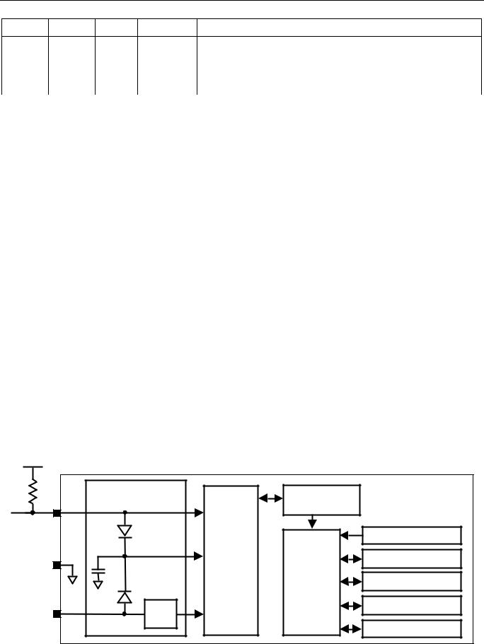
Figure 1 shows a block diagram of the DS18B20, and pin descriptions are given in Table 1. The 64-bit ROM stores the device’s unique serial code. The scratchpad memory contains the 2-byte temperature register that stores the digital output from the temperature sensor. In addition, the scratchpad provides access to the 1-byte upper and lower alarm trigger registers (TH and TL), and the 1-byte configuration register. The configuration register allows the user to set the resolution of the temperature-to-digital conversion to 9, 10, 11, or 12 bits. The TH, TL and configuration registers are nonvolatile (EEPROM), so they will retain data when the device is powered down.
The DS18B20 uses Dallas’ exclusive 1-Wire bus protocol that implements bus communication using one control signal. The control line requires a weak pullup resistor since all devices are linked to the bus via a 3-state or open-drain port (the DQ pin in the case of the DS18B20). In this bus system, the microprocessor (the master device) identifies and addresses devices on the bus using each device’s unique 64-bit code. Because each device has a unique code, the number of devices that can be addressed on one bus is virtually unlimited. The 1-Wire bus protocol, including detailed explanations of the commands and “time slots,” is covered in the 1-WIRE BUS SYSTEM section of this datasheet.
Another feature of the DS18B20 is the ability to operate without an external power supply. Power is instead supplied through the 1-Wire pullup resistor via the DQ pin when the bus is high. The high bus signal also charges an internal capacitor (CPP), which then supplies power to the device when the bus is low. This method of deriving power from the 1-Wire bus is referred to as “parasite power.” As an alternative, the DS18B20 may also be powered by an external supply on VDD.
DS18B20 BLOCK DIAGRAM Figure 1
VPU
4.7k |
PARASITE POWER |
|
MEMORY CONTROL |
DS18B20 |
|
CIRCUIT |
|
||
|
|
LOGIC |
||
|
|
|
|
|
DQ |
|
|
|
|
|
|
|
|
TEMPERATURE SENSOR |
|
INTERNAL VDD |
64-BIT ROM |
|
ALARM HIGH TRIGGER (TH) |
|
|
AND |
|
|
GND |
CPP |
1-wire PORT |
SCRATCHPAD |
REGISTER (EEPROM) |
|
||||
|
|
|
ALARM LOW TRIGGER (TL) |
|
|
|
|
|
|
|
|
|
|
REGISTER (EEPROM) |
|
POWER |
|
|
CONFIGURATION REGISTER |
VDD |
|
|
(EEPROM) |
|
SUPPLY |
|
|
||
|
|
|
||
|
SENSE |
|
|
8-BIT CRC GENERATOR |
|
|
|
|
|
|
|
2 of 20 |
|
|

DS18B20
OPERATION — MEASURING TEMPERATURE
The core functionality of the DS18B20 is its direct-to-digital temperature sensor. The resolution of the temperature sensor is user-configurable to 9, 10, 11, or 12 bits, corresponding to increments of 0.5 C, 0.25 C, 0.125 C, and 0.0625 C, respectively. The default resolution at power-up is 12-bit. The DS18B20 powers-up in a low-power idle state; to initiate a temperature measurement and A-to-D conversion, the master must issue a Convert T [44h] command. Following the conversion, the resulting thermal data is stored in the 2-byte temperature register in the scratchpad memory and the DS18B20 returns to its idle state. If the DS18B20 is powered by an external supply, the master can issue “read time slots” (see the 1- WIRE BUS SYSTEM section) after the Convert T command and the DS18B20 will respond by transmitting 0 while the temperature conversion is in progress and 1 when the conversion is done. If the DS18B20 is powered with parasite power, this notification technique cannot be used since the bus must be pulled high by a strong pullup during the entire temperature conversion. The bus requirements for parasite power are explained in detail in the POWERING THE DS18B20 section of this datasheet.
The DS18B20 output temperature data is calibrated in degrees centigrade; for Fahrenheit applications, a lookup table or conversion routine must be used. The temperature data is stored as a 16-bit sign-extended two’s complement number in the temperature register (see Figure 2). The sign bits (S) indicate if the temperature is positive or negative: for positive numbers S = 0 and for negative numbers S = 1. If the DS18B20 is configured for 12-bit resolution, all bits in the temperature register will contain valid data. For 11-bit resolution, bit 0 is undefined. For 10-bit resolution, bits 1 and 0 are undefined, and for 9-bit resolution bits 2, 1 and 0 are undefined. Table 2 gives examples of digital output data and the corresponding temperature reading for 12-bit resolution conversions.
TEMPERATURE REGISTER FORMAT Figure 2
|
|
bit 7 |
bit 6 |
bit 5 |
bit 4 |
bit 3 |
bit 2 |
bit 1 |
bit 0 |
LS Byte |
|
23 |
22 |
21 |
20 |
2-1 |
2-2 |
2-3 |
2-4 |
|
|
bit 15 |
bit 14 |
bit 13 |
bit 12 |
bit 11 |
bit 10 |
bit 9 |
bit 8 |
MS Byte |
S |
S |
S |
S |
S |
26 |
25 |
24 |
|
TEMPERATURE/DATA RELATIONSHIP Table 2
TEMPERATURE |
DIGITAL OUTPUT |
DIGITAL OUTPUT |
|
(Binary) |
(Hex) |
+125°C |
0000 0111 1101 0000 |
07D0h |
+85°C* |
0000 0101 0101 0000 |
0550h |
+25.0625°C |
0000 0001 1001 0001 |
0191h |
+10.125°C |
0000 0000 1010 0010 |
00A2h |
+0.5°C |
0000 0000 0000 1000 |
0008h |
0°C |
0000 0000 0000 0000 |
0000h |
-0.5°C |
1111 1111 1111 1000 |
FFF8h |
-10.125°C |
1111 1111 0101 1110 |
FF5Eh |
-25.0625°C |
1111 1110 0110 1111 |
FE6Fh |
-55°C |
1111 1100 1001 0000 |
FC90h |
*The power-on reset value of the temperature register is +85°C
3 of 20

DS18B20
OPERATION — ALARM SIGNALING
After the DS18B20 performs a temperature conversion, the temperature value is compared to the userdefined two’s complement alarm trigger values stored in the 1-byte TH and TL registers (see Figure 3). The sign bit (S) indicates if the value is positive or negative: for positive numbers S = 0 and for negative numbers S = 1. The TH and TL registers are nonvolatile (EEPROM) so they will retain data when the device is powered down. TH and TL can be accessed through bytes 2 and 3 of the scratchpad as explained in the MEMORY section of this datasheet.
TH AND TL REGISTER FORMAT Figure 3
bit 7 |
bit 6 |
bit 5 |
bit 4 |
bit 3 |
bit 2 |
bit 1 |
bit 0 |
S |
26 |
25 |
25 |
25 |
22 |
21 |
20 |
Only bits 11 through 4 of the temperature register are used in the TH and TL comparison since TH and TL are 8-bit registers. If the measured temperature is lower than or equal to TL or higher than TH, an alarm condition exists and an alarm flag is set inside the DS18B20. This flag is updated after every temperature measurement; therefore, if the alarm condition goes away, the flag will be turned off after the next temperature conversion.
The master device can check the alarm flag status of all DS18B20s on the bus by issuing an Alarm Search [ECh] command. Any DS18B20s with a set alarm flag will respond to the command, so the master can determine exactly which DS18B20s have experienced an alarm condition. If an alarm condition exists and the TH or TL settings have changed, another temperature conversion should be done to validate the alarm condition.
POWERING THE DS18B20
The DS18B20 can be powered by an external supply on the VDD pin, or it can operate in “parasite power” mode, which allows the DS18B20 to function without a local external supply. Parasite power is very useful for applications that require remote temperature sensing or that are very space constrained. Figure 1 shows the DS18B20’s parasite-power control circuitry, which “steals” power from the 1-Wire bus via the DQ pin when the bus is high. The stolen charge powers the DS18B20 while the bus is high, and some of the charge is stored on the parasite power capacitor (CPP) to provide power when the bus is low. When the DS18B20 is used in parasite power mode, the VDD pin must be connected to ground.
In parasite power mode, the 1-Wire bus and CPP can provide sufficient current to the DS18B20 for most operations as long as the specified timing and voltage requirements are met (refer to the DC ELECTRICAL CHARACTERISTICS and the AC ELECTRICAL CHARACTERISTICS sections of this data sheet). However, when the DS18B20 is performing temperature conversions or copying data from the scratchpad memory to EEPROM, the operating current can be as high as 1.5mA. This current can cause an unacceptable voltage drop across the weak 1-Wire pullup resistor and is more current than can be supplied by CPP. To assure that the DS18B20 has sufficient supply current, it is necessary to provide a strong pullup on the 1-Wire bus whenever temperature conversions are taking place or data is being copied from the scratchpad to EEPROM. This can be accomplished by using a MOSFET to pull the bus directly to the rail as shown in Figure 4. The 1-Wire bus must be switched to the strong pullup within 10 s (max) after a Convert T [44h] or Copy Scratchpad [48h] command is issued, and the bus must be
held high by the pullup for the duration of the conversion (tconv) or data transfer (twr = 10ms). No other activity can take place on the 1-Wire bus while the pullup is enabled.
The DS18B20 can also be powered by the conventional method of connecting an external power supply to the VDD pin, as shown in Figure 5. The advantage of this method is that the MOSFET pullup is not required, and the 1-Wire bus is free to carry other traffic during the temperature conversion time.
4 of 20
DS18B20
The use of parasite power is not recommended for temperatures above +100 C since the DS18B20 may not be able to sustain communications due to the higher leakage currents that can exist at these temperatures. For applications in which such temperatures are likely, it is strongly recommended that the DS18B20 be powered by an external power supply.
In some situations the bus master may not know whether the DS18B20s on the bus are parasite powered or powered by external supplies. The master needs this information to determine if the strong bus pullup should be used during temperature conversions. To get this information, the master can issue a Skip ROM [CCh] command followed by a Read Power Supply [B4h] command followed by a “read time slot”. During the read time slot, parasite powered DS18B20s will pull the bus low, and externally powered DS18B20s will let the bus remain high. If the bus is pulled low, the master knows that it must supply the strong pullup on the 1-Wire bus during temperature conversions.
SUPPLYING THE PARASITE-POWERED DS18B20 DURING TEMPERATURE
CONVERSIONS Figure 4
VPU
|
DS18B20 |
|
GND DQ VDD |
Micro- |
VPU |
|
|
processor |
4.7k |
|
|
|
1-Wire Bus |
To Other
1-Wire Devices
POWERING THE DS18B20 WITH AN EXTERNAL SUPPLY Figure 5
|
VPU |
|
DS18B20 |
|
VDD (External Supply) |
||||
Micro- |
|
|
|||||||
GND DQ VDD |
|
|
|||||||
|
|
|
|
|
|||||
processor |
|
|
|
|
|
|
|
|
|
|
|
|
|
|
|
|
|
|
|
|
4.7k |
|
|
|
|
|
|
To Other |
|
|
|
1-Wire Bus |
|
||||||
|
|
|
|
||||||
|
|
|
|
1-Wire Devices |
|||||
|
|
|
|
|
|
|
|
|
|
|
|
|
|
|
|
|
|
|
|
64-BIT LASERED ROM CODE
Each DS18B20 contains a unique 64–bit code (see Figure 6) stored in ROM. The least significant 8 bits of the ROM code contain the DS18B20’s 1-Wire family code: 28h. The next 48 bits contain a unique serial number. The most significant 8 bits contain a cyclic redundancy check (CRC) byte that is calculated from the first 56 bits of the ROM code. A detailed explanation of the CRC bits is provided in the CRC GENERATION section. The 64-bit ROM code and associated ROM function control logic allow the DS18B20 to operate as a 1-Wire device using the protocol detailed in the 1-WIRE BUS SYSTEM section of this datasheet.
64-BIT LASERED ROM CODE Figure 6
8-BIT CRC |
|
48-BIT SERIAL NUMBER |
8-BIT FAMILY CODE (28h) |
||
MSB |
LSB MSB |
LSB |
MSB |
LSB |
|
|
|
|
5 of 20 |
|
|

DS18B20
MEMORY
The DS18B20’s memory is organized as shown in Figure 7. The memory consists of an SRAM scratchpad with nonvolatile EEPROM storage for the high and low alarm trigger registers (TH and TL) and configuration register. Note that if the DS18B20 alarm function is not used, the TH and TL registers can serve as general-purpose memory. All memory commands are described in detail in the DS18B20 FUNCTION COMMANDS section.
Byte 0 and byte 1 of the scratchpad contain the LSB and the MSB of the temperature register, respectively. These bytes are read-only. Bytes 2 and 3 provide access to TH and TL registers. Byte 4 contains the configuration register data, which is explained in detail in the CONFIGURATION REGISTER section of this datasheet. Bytes 5, 6, and 7 are reserved for internal use by the device and cannot be overwritten; these bytes will return all 1s when read.
Byte 8 of the scratchpad is read-only and contains the cyclic redundancy check (CRC) code for bytes 0 through 7 of the scratchpad. The DS18B20 generates this CRC using the method described in the CRC GENERATION section.
Data is written to bytes 2, 3, and 4 of the scratchpad using the Write Scratchpad [4Eh] command; the data must be transmitted to the DS18B20 starting with the least significant bit of byte 2. To verify data integrity, the scratchpad can be read (using the Read Scratchpad [BEh] command) after the data is written. When reading the scratchpad, data is transferred over the 1-Wire bus starting with the least significant bit of byte 0. To transfer the TH, TL and configuration data from the scratchpad to EEPROM, the master must issue the Copy Scratchpad [48h] command.
Data in the EEPROM registers is retained when the device is powered down; at power-up the EEPROM data is reloaded into the corresponding scratchpad locations. Data can also be reloaded from EEPROM to the scratchpad at any time using the Recall E2 [B8h] command. The master can issue read time slots following the Recall E2 command and the DS18B20 will indicate the status of the recall by transmitting 0 while the recall is in progress and 1 when the recall is done.
DS18B20 MEMORY MAP Figure 7
|
SCRATCHPAD (Power-up State) |
|
|
|
|
|||
byte 0 |
Temperature LSB (50h) |
|
|
|
|
|
|
|
|
(85°C) |
|
|
|
|
EEPROM |
||
|
|
|
|
|
|
|
||
byte 1 |
Temperature MSB (05h) |
|
|
|
|
|
||
|
|
|
|
|
|
|||
|
|
|
|
|
|
|
|
|
byte 2 |
TH Register or User Byte 1* |
|
|
|
|
|
TH Register or User Byte 1 |
|
|
|
|
|
|
||||
byte 3 |
TL Register or User Byte 2* |
|
|
|
|
|
TL Register or User Byte 2 |
|
|
|
|
|
|
||||
byte 4 |
Configuration Register* |
|
|
|
|
|
Configuration Register |
|
|
|
|
|
|
||||
byte 5 |
Reserved (FFh) |
|
|
|
|
|
|
|
|
|
|
|
|
|
|
|
|
byte 6 |
Reserved (0Ch) |
|
|
|
|
|
|
|
byte 7 |
Reserved (10h) |
|
|
|
|
|
|
|
|
|
|
|
|
|
|
|
|
byte 8 |
CRC* |
|
|
|
|
|
|
|
|
*Power-up state depends on value(s) stored |
|
|
|
|
|||
|
in EEPROM |
|
|
|
|
|
|
|
6 of 20

DS18B20
CONFIGURATION REGISTER
Byte 4 of the scratchpad memory contains the configuration register, which is organized as illustrated in Figure 8. The user can set the conversion resolution of the DS18B20 using the R0 and R1 bits in this register as shown in Table 3. The power-up default of these bits is R0 = 1 and R1 = 1 (12-bit resolution). Note that there is a direct tradeoff between resolution and conversion time. Bit 7 and bits 0 to 4 in the configuration register are reserved for internal use by the device and cannot be overwritten; these bits will return 1s when read.
CONFIGURATION REGISTER Figure 8
bit 7 |
bit 6 |
bit 5 |
bit 4 |
bit 3 |
bit 2 |
bit 1 |
bit 0 |
0 |
R1 |
R0 |
1 |
1 |
1 |
1 |
1 |
|
|
|
|
|
|
|
|
THERMOMETER RESOLUTION CONFIGURATION Table 3
R1 |
R0 |
Resolution |
Max Conversion Time |
|
0 |
0 |
9-bit |
93.75 ms |
(tCONV/8) |
0 |
1 |
10-bit |
187.5 ms |
(tCONV/4) |
1 |
0 |
11-bit |
375 ms |
(tCONV/2) |
1 |
1 |
12-bit |
750 ms |
(tCONV) |
CRC GENERATION
CRC bytes are provided as part of the DS18B20’s 64-bit ROM code and in the 9th byte of the scratchpad memory. The ROM code CRC is calculated from the first 56 bits of the ROM code and is contained in the most significant byte of the ROM. The scratchpad CRC is calculated from the data stored in the scratchpad, and therefore it changes when the data in the scratchpad changes. The CRCs provide the bus master with a method of data validation when data is read from the DS18B20. To verify that data has been read correctly, the bus master must re-calculate the CRC from the received data and then compare this value to either the ROM code CRC (for ROM reads) or to the scratchpad CRC (for scratchpad reads). If the calculated CRC matches the read CRC, the data has been received error free. The comparison of CRC values and the decision to continue with an operation are determined entirely by the bus master. There is no circuitry inside the DS18B20 that prevents a command sequence from proceeding if the DS18B20 CRC (ROM or scratchpad) does not match the value generated by the bus master.
The equivalent polynomial function of the CRC (ROM or scratchpad) is:
CRC = X8 + X5 + X4 + 1
The bus master can re-calculate the CRC and compare it to the CRC values from the DS18B20 using the polynomial generator shown in Figure 9. This circuit consists of a shift register and XOR gates, and the shift register bits are initialized to 0. Starting with the least significant bit of the ROM code or the least significant bit of byte 0 in the scratchpad, one bit at a time should shifted into the shift register. After shifting in the 56th bit from the ROM or the most significant bit of byte 7 from the scratchpad, the polynomial generator will contain the re-calculated CRC. Next, the 8-bit ROM code or scratchpad CRC from the DS18B20 must be shifted into the circuit. At this point, if the re-calculated CRC was correct, the shift register will contain all 0s. Additional information about the Dallas 1-Wire cyclic redundancy check
7 of 20

DS18B20
is available in Application Note 27: Understanding and Using Cyclic Redundancy Checks with Dallas Semiconductor Touch Memory Products.
CRC GENERATOR Figure 9
INPUT
XOR |
XOR |
XOR |
(MSB) |
|
(LSB) |
1-WIRE BUS SYSTEM
The 1-Wire bus system uses a single bus master to control one or more slave devices. The DS18B20 is always a slave. When there is only one slave on the bus, the system is referred to as a “single-drop” system; the system is “multidrop” if there are multiple slaves on the bus.
All data and commands are transmitted least significant bit first over the 1-Wire bus.
The following discussion of the 1-Wire bus system is broken down into three topics: hardware configuration, transaction sequence, and 1-Wire signaling (signal types and timing).
HARDWARE CONFIGURATION
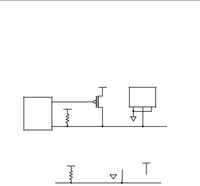
The 1-Wire bus has by definition only a single data line. Each device (master or slave) interfaces to the data line via an open-drain or 3-state port. This allows each device to “release” the data line when the device is not transmitting data so the bus is available for use by another device. The 1-Wire port of the DS18B20 (the DQ pin) is open drain with an internal circuit equivalent to that shown in Figure 10.
The 1-Wire bus requires an external pullup resistor of approximately 5k ; thus, the idle state for the 1- Wire bus is high. If for any reason a transaction needs to be suspended, the bus MUST be left in the idle state if the transaction is to resume. Infinite recovery time can occur between bits so long as the 1-Wire bus is in the inactive (high) state during the recovery period. If the bus is held low for more than 480 s, all components on the bus will be reset.
HARDWARE CONFIGURATION Figure 10
VPU
|
DS18B20 1-WIRE PORT |
|
4.7k |
DQ |
|
1-Wire Bus |
Pin |
RX |
|
||
RX |
|
|
|
5µA |
TX |
|
Typ. |
|
TX |
|
100 |
|
|
MOSFET |
RX = RECEIVE |
|
|
TX = TRANSMIT |
|
|
8 of 20

DS18B20
TRANSACTION SEQUENCE
The transaction sequence for accessing the DS18B20 is as follows: Step 1. Initialization
Step 2. ROM Command (followed by any required data exchange)
Step 3. DS18B20 Function Command (followed by any required data exchange)
It is very important to follow this sequence every time the DS18B20 is accessed, as the DS18B20 will not respond if any steps in the sequence are missing or out of order. Exceptions to this rule are the Search ROM [F0h] and Alarm Search [ECh] commands. After issuing either of these ROM commands, the master must return to Step 1 in the sequence.
INITIALIZATION
All transactions on the 1-Wire bus begin with an initialization sequence. The initialization sequence consists of a reset pulse transmitted by the bus master followed by presence pulse(s) transmitted by the slave(s). The presence pulse lets the bus master know that slave devices (such as the DS18B20) are on the bus and are ready to operate. Timing for the reset and presence pulses is detailed in the
1-WIRE SIGNALING section.
ROM COMMANDS
After the bus master has detected a presence pulse, it can issue a ROM command. These commands operate on the unique 64-bit ROM codes of each slave device and allow the master to single out a specific device if many are present on the 1-Wire bus. These commands also allow the master to determine how many and what types of devices are present on the bus or if any device has experienced an alarm condition. There are five ROM commands, and each command is 8 bits long. The master device must issue an appropriate ROM command before issuing a DS18B20 function command. A flowchart for operation of the ROM commands is shown in Figure 11.
SEARCH ROM [F0h]
When a system is initially powered up, the master must identify the ROM codes of all slave devices on the bus, which allows the master to determine the number of slaves and their device types. The master learns the ROM codes through a process of elimination that requires the master to perform a Search ROM cycle (i.e., Search ROM command followed by data exchange) as many times as necessary to identify all of the slave devices. If there is only one slave on the bus, the simpler Read ROM command (see below) can be used in place of the Search ROM process. For a detailed explanation of the Search ROM procedure, refer to the iButton® Book of Standards at www.ibutton.com/ibuttons/standard.pdf. After every Search ROM cycle, the bus master must return to Step 1 (Initialization) in the transaction sequence.
READ ROM [33h]
This command can only be used when there is one slave on the bus. It allows the bus master to read the slave’s 64-bit ROM code without using the Search ROM procedure. If this command is used when there is more than one slave present on the bus, a data collision will occur when all the slaves attempt to respond at the same time.
MATCH ROM [55h]
The match ROM command followed by a 64-bit ROM code sequence allows the bus master to address a specific slave device on a multidrop or single-drop bus. Only the slave that exactly matches the 64-bit ROM code sequence will respond to the function command issued by the master; all other slaves on the bus will wait for a reset pulse.
iButton is a registered trademark of Dallas Semiconductor.
9 of 20

DS18B20
SKIP ROM [CCh]
The master can use this command to address all devices on the bus simultaneously without sending out any ROM code information. For example, the master can make all DS18B20s on the bus perform simultaneous temperature conversions by issuing a Skip ROM command followed by a Convert T [44h] command.
Note that the Read Scratchpad [BEh] command can follow the Skip ROM command only if there is a single slave device on the bus. In this case time is saved by allowing the master to read from the slave without sending the device’s 64-bit ROM code. A Skip ROM command followed by a Read Scratchpad command will cause a data collision on the bus if there is more than one slave since multiple devices will attempt to transmit data simultaneously.
ALARM SEARCH [ECh]
The operation of this command is identical to the operation of the Search ROM command except that only slaves with a set alarm flag will respond. This command allows the master device to determine if any DS18B20s experienced an alarm condition during the most recent temperature conversion. After every Alarm Search cycle (i.e., Alarm Search command followed by data exchange), the bus master must return to Step 1 (Initialization) in the transaction sequence. Refer to the OPERATION — ALARM SIGNALING section for an explanation of alarm flag operation.
DS18B20 FUNCTION COMMANDS
After the bus master has used a ROM command to address the DS18B20 with which it wishes to communicate, the master can issue one of the DS18B20 function commands. These commands allow the master to write to and read from the DS18B20’s scratchpad memory, initiate temperature conversions and determine the power supply mode. The DS18B20 function commands, which are described below, are summarized in Table 4 and illustrated by the flowchart in Figure 12.
CONVERT T [44h]
This command initiates a single temperature conversion. Following the conversion, the resulting thermal data is stored in the 2-byte temperature register in the scratchpad memory and the DS18B20 returns to its low-power idle state. If the device is being used in parasite power mode, within 10 s (max) after this command is issued the master must enable a strong pullup on the 1-Wire bus for the duration of the conversion (tconv) as described in the POWERING THE DS18B20 section. If the DS18B20 is powered by an external supply, the master can issue read time slots after the Convert T command and the DS18B20 will respond by transmitting a 0 while the temperature conversion is in progress and a 1 when the conversion is done. In parasite power mode this notification technique cannot be used since the bus is pulled high by the strong pullup during the conversion.
WRITE SCRATCHPAD [4Eh]
This command allows the master to write 3 bytes of data to the DS18B20’s scratchpad. The first data byte is written into the TH register (byte 2 of the scratchpad), the second byte is written into the TL register (byte 3), and the third byte is written into the configuration register (byte 4). Data must be transmitted least significant bit first. All three bytes MUST be written before the master issues a reset, or the data may be corrupted.
READ SCRATCHPAD [BEh]
This command allows the master to read the contents of the scratchpad. The data transfer starts with the least significant bit of byte 0 and continues through the scratchpad until the 9th byte (byte 8 – CRC) is read. The master may issue a reset to terminate reading at any time if only part of the scratchpad data is needed.
10 of 20