

диафрагмированные волноводные фильтры / 56ea7d40-8273-4c5a-b38a-6f5402a665ad
.pdfwww.ietdl.org
Published in IET Microwaves, Antennas & Propagation Received on 7th August 2013
Revised on 29th November 2013 Accepted on 8th January 2014 doi: 10.1049/iet-map.2013.0431
ISSN 1751-8725
Compact high-power broadband absorptive filters using slotted waveguide harmonic pads
Tinus Stander, Petrie Meyer, Pieter Willem van der Walt
Department of Electrical and Electronics Engineering, University of Stellenbosch, Private Bag X1, 7602 Matieland, South Africa
E-mail: pmeyer@sun.ac.za
Abstract: A compact high-power broadband absorptive filter is designed by cascading a slotted waveguide harmonic pad with a wide stop-band reflective filter. Absorption is achieved by coupling a surface current standing wave to absorptive external auxiliary waveguides through a cascade of transversal broadwall slots in rectangular waveguide.
1 Introduction
Absorptive microwave filters achieve out-of-band attenuation by partial absorption rather than reflection of the signal, allowing for low input reflection coefficients at frequencies outside the passband. These filters find application where reflection of spurious out-of-band signals, typically generated by non-linear circuit elements, are unwanted, yet such signals must be prevented from reaching the output of the device. Typical examples include the output of mixer circuits where the reflected spurious signals can be re-introduced into the mixing process, or high-power transmitters where the reflected spurious signals can damage or de-stabilise the output amplifiers [1]. A fundamental requirement of these filters is therefore the existence of a second signal path through which only out-of-band signals are routed to internal or external absorbers (instead of being reflected back to the source), to form a frequency selective absorber.
For low-power applications, a few classes of such absorptive filters have been proposed in the literature. A common approach is to load one port of a circulator or hybrid network with a frequency selective absorber which reflects energy outside of the frequency band of absorption [2, 3]. Signals within the desired filter passband are reflected from this network and routed to an output port via the circulator or hybrid network. Another popular class of filter is based on structures which create dual-phase path cancellation [4], with approaches using digital spectrum shaping filters [5] also used. For applications requiring both a wide stop-band and high-power handling capability, however, the most common solution by far is the ‘leaky wall filter’ [6, 7]. These filters attenuate an incident travelling wave in waveguide by coupling energy to an exterior structure through a series of appropriate apertures, usually narrow slots. The exterior structure may either be longitudinal auxiliary waveguides placed in parallel to the main guide [6] or individual waveguides for each aperture [7].
IET Microw. Antennas Propag., 2014, Vol. 8, Iss. 9, pp. 673–678 doi: 10.1049/iet-map.2013.0431
In both cases, the passband cut-off is determined by the cut-off frequency of the auxiliary waveguides, above which the energy from the main guide is coupled to the auxiliary guides and dissipated inside absorptive loads terminating the guides. This approach is highly effective, and current high-end commercial X-band absorptive filters achieve out-of-band attenuation levels of better than 40 dB and out-of-band reflection coefficients of better than −7.5 dB over a frequency band covering three harmonics, while able to handle continuous-wave power levels of up to 500 W and peak power levels of up to 5 kW peak [8]. However, these filters suffer from two main drawbacks, that is, that they are normally very bulky, and that the design process allows for very little control over the shape of the passband reflection response. Alternative approaches using cascades of high-power lossy resonators have been proposed [9–11], but no general synthesis theory exists whereby these resonators can be utilised to design absorptive filters.
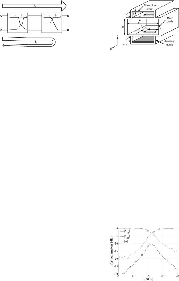
If absorption is only required in specific frequency bands in the stop-band of the filter, as is the case with the widely used harmonic filters at the outputs of transmitters, a particular approach using so-called harmonic pads [12] is of interest. A harmonic pad is effectively any device that features frequency selective absorption in a specific band and lossless transmission elsewhere. If such a device is inserted in front of a standard lossless reflective filter as shown in Fig. 1, the signals in the passband of the reflective filter are passed with very little attenuation, whereas the signals in the stop-band are reflected and selectively absorbed by the harmonic pad. The combined system therefore only exhibits a low input reflection coefficient in the filter passband and all bands in which absorption takes place, but as there is no requirement in this class of applications for low reflection outside of these bands, such a solution fulfils the system requirements. In addition, it has the significant advantage that the reflecting filter provides the stop-band attenuation for the system, while the amount of power absorbed need only be sufficient to protect the output of the source and/or
673 & The Institution of Engineering and Technology 2014
www.ietdl.org
Fig. 1 Block diagram of cascaded harmonic pad and reflective filter
Solid lines show S21 and dotted lines S11
prevent non-linear source behaviour because of the reflected power. Such an approach, but without implementation, has been proposed by various authors [7, 13, 14]. Implementations using 0 dB couplers over the signal bandwidth have been published [12], but these limit the filter transmission bandwidth to that achievable by the coupler. The use of leaky wall filters as harmonic pads has been suggested [5], but not developed in the literature to date.
This paper develops a high-power broadband absorptive filter by cascading a novel distributed harmonic pad, consisting of a compact slotted waveguide structure, with a lossless reflective filter with a wide stop-band, both in WR-90 waveguide. A non-uniform waffle-iron filter is used as a reflective filter [1], although any reflective filter can be used in principle. The slotted waveguide structure (similar to a slotted waveguide antenna, but with varying slot lengths) is designed to absorb the standing wave created by the reflective filter at a number of frequencies in the stop-band of the reflective filter, without affecting the passband response of the system. Using this combination, an absorptive filter is realised without the use of circulators, hybrid circuits or dual signal paths. In comparison with the standard leaky-wave filters, which utilise the systematic absorption of a travelling wave to create both out-of-band attenuation and absorption of any reflected signals, the solution proposed here utilises reflection from a standard filter to implement out-of-band attenuation, and resonant absorbers, designed to cover the frequency bands of interest, to implement partial absorption of the reflected signals. In this way, the absorption levels comparable with that reported in state-of-the-art leaky-wave filters can be achieved with a structure which is significantly more compact. As an example, a very compact harmonic pad is
designed and tested at X-band. The |
pad measures only |
33 mm in length, yet when combined |
with the reflective |
filter, yields a reflection coefficient of |
below −12.5 dB in |
the stop band while attenuating the signal by better than 65 dB. In all the cases, circuit simulation is done using AWR Microwave Office, and full-wave simulation using CST Microwave Studio.
2 Transversal broadwall slots in rectangular waveguide
For use as a harmonic pad, a single waveguide slot should extract as much of the reflected energy from the main guide as possible over a specific frequency band, without affecting the passband transmission at other frequencies. The ideal slot should also be orientated in such a way as to
674
& The Institution of Engineering and Technology 2014
Fig. 2 Transversal broadwall slot pair with auxiliary waveguides
reduce the overall length of the complete structure by as much as possible. To avoid excitation of higher order modes, slot arrangements that preserve both E-plane and H-plane symmetry are preferred.
A topology that satisfies all the above conditions, is the transversal broadwall slot [15], which has been shown to achieve coupling values of up to −6 dB, with a 3 dB bandwidth of 17% [16]. If a symmetric pair of centred, non-inclined slots is placed as shown in Fig. 2, both the E-plane and H-plane symmetries are preserved. The width of the auxiliary guide can be reduced to increase the TE10 cut-off frequency of the auxiliary guide to above the main guide frequency band. This creates a natural high-pass filtering effect which inhibits energy flow to the auxiliary guide below this frequency. To absorb the power in the auxiliary guide, the broadwall of this guide is lined with an absorptive sheet of thickness ta = 1 mm and the guide is terminated at both ends with matched absorbers.
The performance of such a slot pair is illustrated in Fig. 3, which shows the full-wave simulation results of a single, isolated pair of slots of length l = 8 mm and width w = 1 mm, coupling a standard X-band waveguide of wall thickness t = 1 mm to a reduced auxiliary guide of dimension 13 × 3 mm2 through each broadwall, with the auxiliary guides terminated at both ends with a perfect waveguide port. Defining absorption as in (1)
A = 1 − S11 |
|
2 |
− S21 |
|
2 |
(1) |
|
|
|
|
|
||
|
|
|
|
|
|
|
it is clear that this configuration achieves a peak absorption of −3.69 dB over a 3 dB bandwidth of 16.5% around
Fig. 3 Transmission, reflection and absorption of transversal broadwall slot pair (l = 8 mm, w = 1 mm, t = 1 mm, a = 22.86 mm, b = 10.16 mm, á = 13 mm, b´ = 3 mm)
IET Microw. Antennas Propag., 2014, Vol. 8, Iss. 9, pp. 673–678 doi: 10.1049/iet-map.2013.0431
19.22 GHz, and a reflection coefficient of below −29 dB across the band 8.5–10.5 GHz. Parameter studies show that in general, the slot length l determines the frequency of maximum coupling, while the bandwidth is adjusted by varying the slot width w and wall thickness t. Variation in peak absorption cannot be achieved by rotating or moving the slot from the centre axis, since this would disrupt the E-plane symmetry required to avoid the excitation of propagating even modes. However, for a fixed slot length, |A|peak can be adjusted by varying the auxiliary guide height b′.
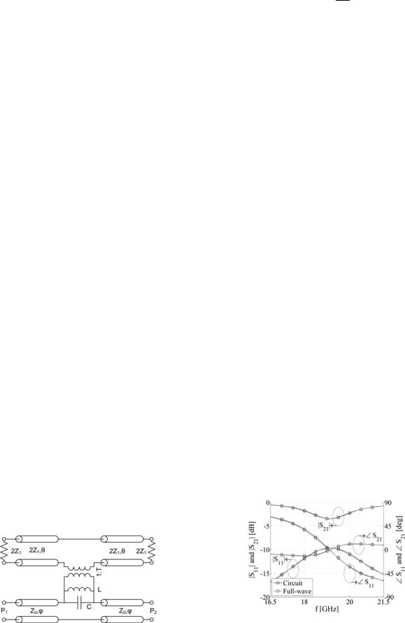
3 Circuit model
Single transversal coupling slots have been studied extensively in the literature, with the original classical models proposed by Oliner [17] expanded more recently using models based on full-wave electromagnetic simulations [15]. In this paper, the simple model shown in Fig. 4 is proposed for a single symmetric pair of slots such as depicted in Fig. 2. Here, the main guide is represented as a transmission line with characteristic impedance Z0, the auxiliary guides as transmission lines of length θ1 and characteristic impedance Z1, terminated on both sides by a load Z1, and the reactive coupling as a transformer and resonant circuit. To model coupling through both the floor and the roof of the main guide, one can either use two coupled circuits in series, or one coupled circuit with all the impedances doubled, as shown in Fig. 4. The latter is possible as the impedance presented to the main guide simply doubles when using slots in both broad walls.
This model is based on that of Eshrah et al. [15], but is reduced in complexity by the use of a single resonator, rather than two coupled resonators connected by a finite length of transmission line. In this, it is assumed that the thickness of the waveguide wall, which is modelled in [15] with a finite length transmission line, is negligible at the frequencies of interest. To determine the equivalent circuit element values, the scattering parameters of the physical structure are calculated through full-wave electromagnetic simulation, with P2 and P1 terminated by ideal waveguide ports. The resonator parameters are related simply by the resonant frequency
1
v0 = √ (2)
LC
at which the phase values of S11 and S21 are equal. At this frequency, L and C cancel, and the transformer and terminated auxiliary guide can be represented by a single resistor of value R, which is related to the transformer turns
www.ietdl.org
ration T by
T = 4Z1 (3)
R
with port P2 of both the physical structure and the equivalent circuit terminated in a matched load, and port P1 de-embedded to the centre of the symmetric coupling slots for both cases (i.e. by distance j for the equivalent circuit), the input impedance at port P1 is purely resistive at resonance. At the resonant frequency, the resistance R is then calculated from the simulated input reflection coefficient |Γ| = |S11| as
2Z0|G|v=v0 |
(4) |
R = 1 − |G|v=v0 |
Although it is possible to calculate L or C from the slope of the input reflection coefficient against frequency at resonance, or the wideband response of either S11 or S21, both of these methods rely heavily on the accuracy of a few data points in a full-wave simulation, and are complicated by the presence of the embedding transmission line. A better broadband approximation is made by deriving the magnitude of the input reflection coefficient of the equivalent circuit (as referred to the de-embedded input port in the main guide) from circuit theory as
|G| = |
|
|
|
|
vLR |
|
|
|
|
|
(5) |
|
|
|
|
|
|
|
|
|
|
|
|
||
|
2RZ0 |
− 2v2 |
RZ0 |
/v02 |
|
2 |
+ Lv 2Z0 |
+ R |
|
2 |
||
|
|
|||||||||||
|
|
|
|
|
|
|
|
|
|
|
|
|
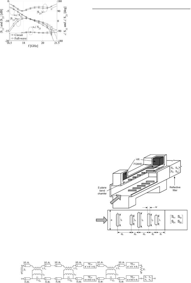
The value of L (and C through (3)) is determined by obtaining simulated values of |Γ| over a 25% band around the resonant frequency, and minimising the root-mean-square (RMS) error between the full-wave simulated and circuit simulated values of |Γ|. Finally, a value for j is found by equating the transmission phase response of the full-wave simulated transmission line S21 to that of the circuit model. To illustrate this method of modelling, the full-wave S-parameters of the example structure in Fig. 2 (l = 8, w = 1, t = 1, a = 22.86, b = 10.16, a′ = 13, b′ = 3) are shown in Fig. 5, together with the S-parameters of the derived model (T = 2.20, L = 400 fH, C = 173 pF, j = 0.28°). It is evident that good agreement between full-wave and circuit models is achieved. Using two of these single-slot models separated by an ideal model of a section of TE10 waveguide, a combination of two of the same slots as in the previous example, cascaded with a spacing of 5 mm, is also
|
Fig. 5 Performance of single resonator approximation of 8 mm |
Fig. 4 Circuit model of a single transversal broadwall slot pair |
transversal coupling slot pair |
IET Microw. Antennas Propag., 2014, Vol. 8, Iss. 9, pp. 673–678 |
675 |
doi: 10.1049/iet-map.2013.0431 |
& The Institution of Engineering and Technology 2014 |
www.ietdl.org
Table 1 Optimised circuit parameters and associated physical
dimensions |
|
|
|
|
|
|
|
Slot # |
f, GHz |
L, fH |
C, pF |
T |
j, deg |
l, mm |
d, mm |
1 |
22.49 |
260 |
193 |
2.39 |
−0.45 |
6.75 |
10.81 |
2 |
18.15 |
487 |
158 |
2.13 |
−0.44 |
8.45 |
3.87 |
3 |
20.35 |
351 |
174 |
2.23 |
−0.44 |
7.5 |
2.65 |
4 |
21.00 |
306 |
188 |
2.30 |
−0.44 |
7.25 |
3.86 |
5 |
22.11 |
286 |
181 |
2.35 |
−0.44 |
6.87 |
2.58 |
|
|
|
|
|
|
|
|
Fig. 6 Performance of cascaded coupled resonator circuit to model two slot pairs separated by 5 mm
modelled, with the results shown in Fig. 6. In both cases, the frequency range is selected to represent the second harmonic of an X-band signal, and good agreement in both broadband magnitude and phase response is achieved.
4 Synthesis example
The most applicable synthesis theories for the cascaded absorptive resonators is that of Jaumann absorbers [18], which relies on analytical expressions which grow exponentially more complex for higher network orders, and is unable to accommodate arbitrary terminations. In the absence of a viable synthesis theory for the more general case, circuit model optimisation must be used to synthesise the harmonic pad. Fig. 7 shows the circuit model for a triple slot structure, including the circuit simulation models of perfect TE10 mode waveguides, cascaded with the S-parameters of a given reflective filter.
The synthesis starts by setting the initial values of the resonant frequencies fi for all of the cascaded resonators to the centre frequency of the absorbing band, designated as f0. Initial values of a, b, a′ and b′ are based on the previously chosen values of the main and auxiliary waveguides, with initial values of Li, Ci, ji and Ti derived from the previous comparison between circuit simulated and full-wave simulated responses of a single slot. This necessitates prior full-wave simulation and circuit element value definition of a single slot at the centre of the required absorbing band, as was done in Section 3. Slot spacings di (shown in Fig. 7) are chosen to place the slots at the standing wave pattern maxima at f0 based on the complex input reflection of the reflective filter at f0 and the assumption that local maxima are formed every λg0/2, where λg0 is the guide wavelength at f0. The circuit is then cascaded with the S-parameters of the given reflective filter and the values fi and di are optimised to achieve a goal input reflection match over a given band using a random localised optimisation algorithm. It should be noted that each optimisation update of fi (the slot resonant frequency), and the associated update of the relevant slot length, in actual fact requires an update of all the equivalent circuit
elements for that slot, which in turn requires one full-wave simulation of the updated slot. For small changes in slot length, this step can be omitted as the other parameters are significantly less sensitive to slot length than fi. However, any large change requires a new full-wave simulation. An alternative is to establish values of L, C, j and T for a wide range of slot resonant frequencies (and, therefore, a wide range of slot lengths l ) before circuit optimisation, and apply these changes periodically to the circuit model during optimisation using interpolation-based methods. The synthesis is considered complete when the optimisation goals are achieved with values Li, Ci, ji and Ti that match the final optimised resonant frequency of each slot. The resonant frequencies are then used to find slot lengths li, and used in conjunction with the values of di to construct a full-wave model of the harmonic pad. These dimensions can then be fine-tuned in full-wave simulation to establish a final manufacturing model. Owing to the accuracy of the model, in practice, this tuning process results in dimensional changes of <10% in any of the dimensions.
As an example, the procedure outlined above was applied to design a harmonic pad for an X-band (8.5–10.5 GHz
Fig. 8 Final harmonic pad
Note the two end-loads to the auxiliary guide made from Eccosorb™ HR and placed in E-plane bends
Fig. 7 Triple slot circuit model cascaded with the reflective filter
676 |
IET Microw. Antennas Propag., 2014, Vol. 8, Iss. 9, pp. 673–678 |
& The Institution of Engineering and Technology 2014 |
doi: 10.1049/iet-map.2013.0431 |
www.ietdl.org
Table 2 Initial and manufactured dimensions
Dimension |
l1 |
l2 |
l3 |
l4 |
l5 |
d1 |
d2 |
d3 |
d4 |
d5 |
initial, mm |
6.75 |
8.45 |
7.5 |
7.25 |
6.87 |
10.8 |
3.87 |
2.65 |
3.86 |
2.58 |
tuned, mm |
6.42 |
8.45 |
7.5 |
7.23 |
6.87 |
10.2 |
3.75 |
2.42 |
3.60 |
2.65 |
variation, % |
−4.89 |
0 |
0 |
−0.28 |
0 |
−5.64 |
−3.10 |
−8.68 |
−6.74 |
+ 2.71 |
|
|
|
|
|
|
|
|
|
|
|
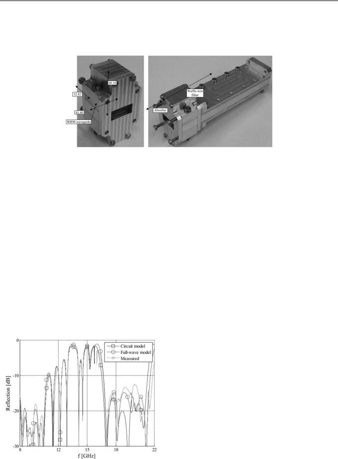
Fig. 9 Manufactured harmonic pad (left) and applied to a reflective waffle-iron filter [1] (right)
passband) filter of which the second harmonic band (17–21 GHz) is to be absorbed and not reflected. An input reflection match of −15 dB across the absorptive band was used as goal function for a five-slot structure. The full-wave simulated S-parameter data of a reflective non-uniform waffle-iron filter was used as termination of the circuit model, as shown in Fig. 7. This filter utilises rectangular waveguide of constant width, and constant height for each section, but non-uniform boss dimensions in order to reduce the size [1]. For the harmonic pad, a minimum slot spacing of di > 2.4 mm was imposed in simulation, to allow for manufacturing. The initial offset d1 was constrained as d1 > 7.9 mm, to allow for flange and an absorptive end-load to the auxiliary guide. The auxiliary guide dimensions of 13 × 3 mm2 were retained, as well as the 1 mm wall thickness and 1 mm slot width. This optimisation produces the circuit values and dimensions shown in Table 1, with the associated S-parameters in Fig. 10. The corresponding physical structure is shown in Fig. 8, with the dimensions listed in Table 2.
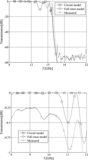
Fig. 10 Measured and simulated reflection response
IET Microw. Antennas Propag., 2014, Vol. 8, Iss. 9, pp. 673–678 doi: 10.1049/iet-map.2013.0431
The final dimensions were obtained after a short additional full-wave optimisation stage aimed at reducing the reflection in the absorption band, during which no dimension had to be tuned by > 10% of its initial value. The full-wave analysis of the final structure is shown in Figs. 9 and 10. It is clear that the technique produces an absorptive filter with good matching in both the passband and absorptive band.
5 Peak power handling capability
The peak power handling capability of the structure is determined by finding the maximum E-field strength Emax, and comparing it to the breakdown E-field strength EB. From simulation, the maximum E-field occurs at resonance across the slot aperture. At 19 GHz, the simulation indicates Emax = 36996 V/m RMS for 1 W RMS incident power, which translates to a peak incident
power Pmax 1.086 kW if the value of Emax = 12.1 kV/cm RMS is chosen to avoid sparking across the aperture of
the slot. Away from slot resonance, the slot exhibits
maximum power handling |
capabilities |
comparable with |
the waveguide itself, since |
there is no |
concentration of |
E-field in or around the slot. |
|
|
6 Manufacturing and measured results
The harmonic pad was manufactured from Aluminium 6082 (Fig. 9), using Eccosorb™ FGM-40 as sheet absorber lining the opposing broadwall in the auxiliary guide. The absorptive end-loads in the auxiliary guides were implemented with Eccosorb™ HR in an E-plane bend, to make the load (and, consequently, the pad itself) more compact. The harmonic pad has a total length of 33 mm, flanges included. The harmonic pad was attached to an existing non-uniform waffle-iron filter, with the total measured S-parameters shown in Figs. 10–12. Calibration was performed over the bands 8–12 and 16–22 GHz, to cover the transmission and absorption bands of interest. A full two-port coaxial calibration at the coaxial-waveguide transitions was completed, followed by a TRL waveguide
677 & The Institution of Engineering and Technology 2014
www.ietdl.org
Fig. 11 Measured and simulated transmission response, wideband
Fig. 12 Measured and simulated transmission response, narrowband
calibration for, respectively, the two bands of interest. For the TRL calibrations, the line standards were implemented using short sections of WR90 waveguide between the transitions. The complete absorptive filter exhibits −18 dB input reflection across the 8.5–10.5 GHz passband (Fig. 10) and −12.5 dB peak reflection in the absorptive band. The combined structure exhibits insertion loss of > 65 dB in the absorptive band (Fig. 11) but <0.5 dB in the passband (Fig. 12). The discrepancies in the simulated and measured response are attributed to some discrepancy between the full-wave simulated S-parameter data of the reflective filter (used to design the harmonic pad) and the manufactured S-parameter measurement data of the waffle-iron filter. Nevertheless, the results indicate good agreement between the synthesised and measured responses.
678
& The Institution of Engineering and Technology 2014
7 Conclusion
This paper presents an approach for the development of compact harmonic pads using transversal broadwall slots in rectangular waveguide coupling to absorptive auxiliary guides. Good first-iteration synthesis accuracy is achieved in a band 17–21 GHz, producing matching over a 20% bandwidth to below −12.5 dB.
8 Acknowledgments
The authors wish to thank Reutech Radar Systems (Pty) Ltd. for financial support of this project, CST GmbH for the use of CST Microwave Studio and Applied Wave Research Inc. for the use of AWR Microwave Office.
9References
1Stander, T.: ‘High-power broadband absorptive waveguide filters’. PhD dissertation, University of Stellenbosch, 2009. Available online http:// scholar.sun.ac.za/handle/10019.1/1157
2Rhodes, J.D.: ‘Microwave reflection filter including a ladder network of resonators having progressively smaller Q values’. U.S. Patent 5 781 084, July 14 1998
3Torgow, E.N.: ‘Hybrid junction-cutoff waveguide filters’, IRE Trans. Microw. Theory Tech., 1959, 7, pp. 163–167
4Jachowski, D.R.: ‘Passive enhancement of resonator Q in microwave notch filters’. IEEE MTT-S Int. Microwave Symp. Digest, 2004, vol. 3, pp. 1315–1318
5Djordjevic, A.R., Zajic, A.G.: ‘Low-reflection bandpass filters with a flat
group delay’, IEEE Trans. Microw. Theory Tech., 2005, 53, pp. 1164–1167
6Conning, S.: ‘High-power harmonic suppression filters’. U.S. Patent 3 496 497, February 17 1970
7Met, V.O.: ‘Absorptive filters for microwave harmonic power’, Proc. IRE, 1959, 47, pp. 1762–1769
8ME Corporation. Waveguide harmonic absorption filters, Data Sheet T41C (2005)
9Minakova, L.B., Rud, L.A.: ‘Resonance absorption in single and cascaded lossy waveguide-dielectric resonators’, Microw. Opt. Technol. Lett., 2003, 36, pp. 122–126
10Minakova, L.B., Rud, L.A.: ‘Natural-frequency approach to the synthesis of narrow-band waveguide absorption filters’. Proc. 32nd European Microwave Conf. 2002, vol. 1, pp. 1–4
11Tantawi, S.G., Vlieks, A.E.: ‘Compact X-band high power load using magnetic stainless steel’. Proc. 1995 Particle Accelerator Conf., 1995, vol. 4, pp. 2132–2134
12Young, L.: ‘Waveguide 0-db and 3-db directional couplers as harmonic pads’, Microw. J., 1964, 7, pp. 79–87
13Young, L., Schiffman, B.M., Cristal, E.G.: ‘High-power filters for the suppression of spurious frequencies’. PTGMTT Int. Symp. Digest, 1964, vol. 64
14Young, L.: ‘The design of branch-guide couplers, with applications to the suppression of spurious frequencies’. PGMTT National Symp. Digest, 1962, vol. 62
15Eshrah, I.A., Kishk, A.A., Yakovlev, A.B., Glisson, A.W.: ‘Generalized
equivalent circuit model for transverse waveguide slots and applications’, Prog. Electromagn., 2007, 69, pp. 1–20
16Datta, A., Rajeek, A.M., Chakrabarty, A., Das, B.N.: ‘S-matrix of a broad wall coupler between dissimilar rectangular waveguides’, IEEE Trans. Circuit Theory, 1995, 43, pp. 56–62
17Oliner, A.A.: ‘The impedance properties of narrow radiating slots in the broad face of rectangular waveguide: part II’, IRE Trans. Antennas Propag., 1957, 5, pp. 4–11
18du Toit, L.J.: ‘Advances in the design of Jaumann absorbers’. Proc. IEEE APS Int. Symp., 1990, vol. 3
IET Microw. Antennas Propag., 2014, Vol. 8, Iss. 9, pp. 673–678 doi: 10.1049/iet-map.2013.0431