

- •Features
- •1. Pin Configurations
- •1.1 Pin Descriptions
- •1.1.3 Port B (PB7:0) XTAL1/XTAL2/TOSC1/TOSC2
- •1.1.4 Port C (PC5:0)
- •1.1.5 PC6/RESET
- •1.1.6 Port D (PD7:0)
- •1.1.8 AREF
- •1.1.9 ADC7:6 (TQFP and QFN/MLF Package Only)
- •2. Overview
- •2.1 Block Diagram
- •2.2 Comparison Between ATmega48PA and ATmega88PA
- •3. Resources
- •4. Data Retention
- •5. About Code Examples
- •6. AVR CPU Core
- •6.1 Overview
- •6.2 ALU – Arithmetic Logic Unit
- •6.3 Status Register
- •6.3.1 SREG – AVR Status Register
- •6.4 General Purpose Register File
- •6.5 Stack Pointer
- •6.5.1 SPH and SPL – Stack Pointer High and Stack Pointer Low Register
- •6.6 Instruction Execution Timing
- •6.7 Reset and Interrupt Handling
- •6.7.1 Interrupt Response Time
- •7. AVR Memories
- •7.1 Overview
- •7.3 SRAM Data Memory
- •7.3.1 Data Memory Access Times
- •7.4 EEPROM Data Memory
- •7.4.1 EEPROM Read/Write Access
- •7.4.2 Preventing EEPROM Corruption
- •7.5 I/O Memory
- •7.5.1 General Purpose I/O Registers
- •7.6 Register Description
- •7.6.1 EEARH and EEARL – The EEPROM Address Register
- •7.6.2 EEDR – The EEPROM Data Register
- •7.6.3 EECR – The EEPROM Control Register
- •7.6.4 GPIOR2 – General Purpose I/O Register 2
- •7.6.5 GPIOR1 – General Purpose I/O Register 1
- •7.6.6 GPIOR0 – General Purpose I/O Register 0
- •8. System Clock and Clock Options
- •8.1 Clock Systems and their Distribution
- •8.2 Clock Sources
- •8.2.1 Default Clock Source
- •8.2.2 Clock Startup Sequence
- •8.3 Low Power Crystal Oscillator
- •8.4 Full Swing Crystal Oscillator
- •8.5 Low Frequency Crystal Oscillator
- •8.6 Calibrated Internal RC Oscillator
- •8.7 128 kHz Internal Oscillator
- •8.8 External Clock
- •8.9 Clock Output Buffer
- •8.10 Timer/Counter Oscillator
- •8.11 System Clock Prescaler
- •8.12 Register Description
- •8.12.1 OSCCAL – Oscillator Calibration Register
- •8.12.2 CLKPR – Clock Prescale Register
- •9. Power Management and Sleep Modes
- •9.1 Sleep Modes
- •9.2 BOD Disable
- •9.3 Idle Mode
- •9.4 ADC Noise Reduction Mode
- •9.7 Standby Mode
- •9.8 Extended Standby Mode
- •9.9 Power Reduction Register
- •9.10 Minimizing Power Consumption
- •9.10.1 Analog to Digital Converter
- •9.10.2 Analog Comparator
- •9.10.4 Internal Voltage Reference
- •9.10.5 Watchdog Timer
- •9.10.6 Port Pins
- •9.11 Register Description
- •9.11.1 SMCR – Sleep Mode Control Register
- •9.11.2 MCUCR – MCU Control Register
- •9.11.3 PRR – Power Reduction Register
- •10. System Control and Reset
- •10.1 Resetting the AVR
- •10.2 Reset Sources
- •10.3 Power-on Reset
- •10.4 External Reset
- •10.6 Watchdog System Reset
- •10.7 Internal Voltage Reference
- •10.8 Watchdog Timer
- •10.8.1 Features
- •10.8.2 Overview
- •10.9 Register Description
- •10.9.1 MCUSR – MCU Status Register
- •10.9.2 WDTCSR – Watchdog Timer Control Register
- •11. Interrupts
- •11.1 Interrupt Vectors in ATmega48PA
- •11.2 Interrupt Vectors in ATmega88PA
- •11.3 Register Description
- •11.3.1 Moving Interrupts Between Application and Boot Space, ATmega88PA
- •11.3.2 MCUCR – MCU Control Register
- •12. External Interrupts
- •12.1 Pin Change Interrupt Timing
- •12.2 Register Description
- •12.2.1 EICRA – External Interrupt Control Register A
- •12.2.2 EIMSK – External Interrupt Mask Register
- •12.2.3 EIFR – External Interrupt Flag Register
- •12.2.4 PCICR – Pin Change Interrupt Control Register
- •12.2.5 PCIFR – Pin Change Interrupt Flag Register
- •12.2.6 PCMSK2 – Pin Change Mask Register 2
- •12.2.7 PCMSK1 – Pin Change Mask Register 1
- •12.2.8 PCMSK0 – Pin Change Mask Register 0
- •13. I/O-Ports
- •13.1 Overview
- •13.2 Ports as General Digital I/O
- •13.2.1 Configuring the Pin
- •13.2.2 Toggling the Pin
- •13.2.3 Switching Between Input and Output
- •13.2.4 Reading the Pin Value
- •13.2.5 Digital Input Enable and Sleep Modes
- •13.2.6 Unconnected Pins
- •13.3 Alternate Port Functions
- •13.3.1 Alternate Functions of Port B
- •13.3.2 Alternate Functions of Port C
- •13.3.3 Alternate Functions of Port D
- •13.4 Register Description
- •13.4.1 MCUCR – MCU Control Register
- •13.4.2 PORTB – The Port B Data Register
- •13.4.3 DDRB – The Port B Data Direction Register
- •13.4.4 PINB – The Port B Input Pins Address
- •13.4.5 PORTC – The Port C Data Register
- •13.4.6 DDRC – The Port C Data Direction Register
- •13.4.7 PINC – The Port C Input Pins Address
- •13.4.8 PORTD – The Port D Data Register
- •13.4.9 DDRD – The Port D Data Direction Register
- •13.4.10 PIND – The Port D Input Pins Address
- •14. 8-bit Timer/Counter0 with PWM
- •14.1 Features
- •14.2 Overview
- •14.2.1 Definitions
- •14.2.2 Registers
- •14.3 Timer/Counter Clock Sources
- •14.4 Counter Unit
- •14.5 Output Compare Unit
- •14.5.1 Force Output Compare
- •14.5.2 Compare Match Blocking by TCNT0 Write
- •14.5.3 Using the Output Compare Unit
- •14.6 Compare Match Output Unit
- •14.6.1 Compare Output Mode and Waveform Generation
- •14.7 Modes of Operation
- •14.7.1 Normal Mode
- •14.7.2 Clear Timer on Compare Match (CTC) Mode
- •14.7.3 Fast PWM Mode
- •14.7.4 Phase Correct PWM Mode
- •14.8 Timer/Counter Timing Diagrams
- •14.9 Register Description
- •14.9.1 TCCR0A – Timer/Counter Control Register A
- •14.9.2 TCCR0B – Timer/Counter Control Register B
- •14.9.3 TCNT0 – Timer/Counter Register
- •14.9.4 OCR0A – Output Compare Register A
- •14.9.5 OCR0B – Output Compare Register B
- •14.9.6 TIMSK0 – Timer/Counter Interrupt Mask Register
- •14.9.7 TIFR0 – Timer/Counter 0 Interrupt Flag Register
- •15. 16-bit Timer/Counter1 with PWM
- •15.1 Features
- •15.2 Overview
- •15.2.1 Registers
- •15.2.2 Definitions
- •15.3.1 Reusing the Temporary High Byte Register
- •15.4 Timer/Counter Clock Sources
- •15.5 Counter Unit
- •15.6 Input Capture Unit
- •15.6.1 Input Capture Trigger Source
- •15.6.2 Noise Canceler
- •15.6.3 Using the Input Capture Unit
- •15.7 Output Compare Units
- •15.7.1 Force Output Compare
- •15.7.2 Compare Match Blocking by TCNT1 Write
- •15.7.3 Using the Output Compare Unit
- •15.8 Compare Match Output Unit
- •15.8.1 Compare Output Mode and Waveform Generation
- •15.9 Modes of Operation
- •15.9.1 Normal Mode
- •15.9.2 Clear Timer on Compare Match (CTC) Mode
- •15.9.3 Fast PWM Mode
- •15.9.4 Phase Correct PWM Mode
- •15.9.5 Phase and Frequency Correct PWM Mode
- •15.10 Timer/Counter Timing Diagrams
- •15.11 Register Description
- •15.11.1 TCCR1A – Timer/Counter1 Control Register A
- •15.11.2 TCCR1B – Timer/Counter1 Control Register B
- •15.11.3 TCCR1C – Timer/Counter1 Control Register C
- •15.11.4 TCNT1H and TCNT1L – Timer/Counter1
- •15.11.5 OCR1AH and OCR1AL – Output Compare Register 1 A
- •15.11.6 OCR1BH and OCR1BL – Output Compare Register 1 B
- •15.11.7 ICR1H and ICR1L – Input Capture Register 1
- •15.11.8 TIMSK1 – Timer/Counter1 Interrupt Mask Register
- •15.11.9 TIFR1 – Timer/Counter1 Interrupt Flag Register
- •16. Timer/Counter0 and Timer/Counter1 Prescalers
- •16.1 Internal Clock Source
- •16.2 Prescaler Reset
- •16.3 External Clock Source
- •16.4 Register Description
- •16.4.1 GTCCR – General Timer/Counter Control Register
- •17. 8-bit Timer/Counter2 with PWM and Asynchronous Operation
- •17.1 Features
- •17.2 Overview
- •17.2.1 Registers
- •17.2.2 Definitions
- •17.3 Timer/Counter Clock Sources
- •17.4 Counter Unit
- •17.5 Output Compare Unit
- •17.5.1 Force Output Compare
- •17.5.2 Compare Match Blocking by TCNT2 Write
- •17.5.3 Using the Output Compare Unit
- •17.6 Compare Match Output Unit
- •17.6.1 Compare Output Mode and Waveform Generation
- •17.7 Modes of Operation
- •17.7.1 Normal Mode
- •17.7.2 Clear Timer on Compare Match (CTC) Mode
- •17.7.3 Fast PWM Mode
- •17.7.4 Phase Correct PWM Mode
- •17.8 Timer/Counter Timing Diagrams
- •17.9 Asynchronous Operation of Timer/Counter2
- •17.10 Timer/Counter Prescaler
- •17.11 Register Description
- •17.11.1 TCCR2A – Timer/Counter Control Register A
- •17.11.2 TCCR2B – Timer/Counter Control Register B
- •17.11.3 TCNT2 – Timer/Counter Register
- •17.11.4 OCR2A – Output Compare Register A
- •17.11.5 OCR2B – Output Compare Register B
- •17.11.6 TIMSK2 – Timer/Counter2 Interrupt Mask Register
- •17.11.7 TIFR2 – Timer/Counter2 Interrupt Flag Register
- •17.11.8 ASSR – Asynchronous Status Register
- •17.11.9 GTCCR – General Timer/Counter Control Register
- •18. SPI – Serial Peripheral Interface
- •18.1 Features
- •18.2 Overview
- •18.3 SS Pin Functionality
- •18.3.1 Slave Mode
- •18.3.2 Master Mode
- •18.4 Data Modes
- •18.5 Register Description
- •18.5.1 SPCR – SPI Control Register
- •18.5.2 SPSR – SPI Status Register
- •18.5.3 SPDR – SPI Data Register
- •19. USART0
- •19.1 Features
- •19.2 Overview
- •19.3 Clock Generation
- •19.3.1 Internal Clock Generation – The Baud Rate Generator
- •19.3.2 Double Speed Operation (U2Xn)
- •19.3.3 External Clock
- •19.3.4 Synchronous Clock Operation
- •19.4 Frame Formats
- •19.4.1 Parity Bit Calculation
- •19.5 USART Initialization
- •19.6 Data Transmission – The USART Transmitter
- •19.6.1 Sending Frames with 5 to 8 Data Bit
- •19.6.2 Sending Frames with 9 Data Bit
- •19.6.3 Transmitter Flags and Interrupts
- •19.6.4 Parity Generator
- •19.6.5 Disabling the Transmitter
- •19.7 Data Reception – The USART Receiver
- •19.7.1 Receiving Frames with 5 to 8 Data Bits
- •19.7.2 Receiving Frames with 9 Data Bits
- •19.7.3 Receive Compete Flag and Interrupt
- •19.7.4 Receiver Error Flags
- •19.7.5 Parity Checker
- •19.7.6 Disabling the Receiver
- •19.7.7 Flushing the Receive Buffer
- •19.8 Asynchronous Data Reception
- •19.8.1 Asynchronous Clock Recovery
- •19.8.2 Asynchronous Data Recovery
- •19.8.3 Asynchronous Operational Range
- •19.9.1 Using MPCMn
- •19.10 Register Description
- •19.10.1 UDRn – USART I/O Data Register n
- •19.10.2 UCSRnA – USART Control and Status Register n A
- •19.10.3 UCSRnB – USART Control and Status Register n B
- •19.10.4 UCSRnC – USART Control and Status Register n C
- •19.10.5 UBRRnL and UBRRnH – USART Baud Rate Registers
- •19.11 Examples of Baud Rate Setting
- •20. USART in SPI Mode
- •20.1 Features
- •20.2 Overview
- •20.3 Clock Generation
- •20.4 SPI Data Modes and Timing
- •20.5 Frame Formats
- •20.5.1 USART MSPIM Initialization
- •20.6 Data Transfer
- •20.6.1 Transmitter and Receiver Flags and Interrupts
- •20.6.2 Disabling the Transmitter or Receiver
- •20.7 AVR USART MSPIM vs. AVR SPI
- •20.8 Register Description
- •20.8.1 UDRn – USART MSPIM I/O Data Register
- •20.8.2 UCSRnA – USART MSPIM Control and Status Register n A
- •20.8.3 UCSRnB – USART MSPIM Control and Status Register n B
- •20.8.4 UCSRnC – USART MSPIM Control and Status Register n C
- •20.8.5 USART MSPIM Baud Rate Registers - UBRRnL and UBRRnH
- •21. 2-wire Serial Interface
- •21.1 Features
- •21.2.1 TWI Terminology
- •21.2.2 Electrical Interconnection
- •21.3 Data Transfer and Frame Format
- •21.3.1 Transferring Bits
- •21.3.2 START and STOP Conditions
- •21.3.3 Address Packet Format
- •21.3.4 Data Packet Format
- •21.3.5 Combining Address and Data Packets into a Transmission
- •21.5 Overview of the TWI Module
- •21.5.1 SCL and SDA Pins
- •21.5.2 Bit Rate Generator Unit
- •21.5.3 Bus Interface Unit
- •21.5.4 Address Match Unit
- •21.5.5 Control Unit
- •21.6 Using the TWI
- •21.7 Transmission Modes
- •21.7.1 Master Transmitter Mode
- •21.7.2 Master Receiver Mode
- •21.7.3 Slave Receiver Mode
- •21.7.4 Slave Transmitter Mode
- •21.7.5 Miscellaneous States
- •21.7.6 Combining Several TWI Modes
- •21.9 Register Description
- •21.9.1 TWBR – TWI Bit Rate Register
- •21.9.2 TWCR – TWI Control Register
- •21.9.3 TWSR – TWI Status Register
- •21.9.4 TWDR – TWI Data Register
- •21.9.5 TWAR – TWI (Slave) Address Register
- •21.9.6 TWAMR – TWI (Slave) Address Mask Register
- •22. Analog Comparator
- •22.1 Overview
- •22.2 Analog Comparator Multiplexed Input
- •22.3 Register Description
- •22.3.1 ADCSRB – ADC Control and Status Register B
- •22.3.2 ACSR – Analog Comparator Control and Status Register
- •22.3.3 DIDR1 – Digital Input Disable Register 1
- •23. Analog-to-Digital Converter
- •23.1 Features
- •23.2 Overview
- •23.3 Starting a Conversion
- •23.4 Prescaling and Conversion Timing
- •23.5 Changing Channel or Reference Selection
- •23.5.1 ADC Input Channels
- •23.5.2 ADC Voltage Reference
- •23.6 ADC Noise Canceler
- •23.6.1 Analog Input Circuitry
- •23.6.2 Analog Noise Canceling Techniques
- •23.6.3 ADC Accuracy Definitions
- •23.7 ADC Conversion Result
- •23.8 Temperature Measurement
- •23.9 Register Description
- •23.9.1 ADMUX – ADC Multiplexer Selection Register
- •23.9.2 ADCSRA – ADC Control and Status Register A
- •23.9.3 ADCL and ADCH – The ADC Data Register
- •23.9.3.1 ADLAR = 0
- •23.9.3.2 ADLAR = 1
- •23.9.4 ADCSRB – ADC Control and Status Register B
- •23.9.5 DIDR0 – Digital Input Disable Register 0
- •24. debugWIRE On-chip Debug System
- •24.1 Features
- •24.2 Overview
- •24.3 Physical Interface
- •24.4 Software Break Points
- •24.5 Limitations of debugWIRE
- •24.6 Register Description
- •24.6.1 DWDR – debugWire Data Register
- •25. Self-Programming the Flash, ATmega48PA
- •25.1 Overview
- •25.1.1 Performing Page Erase by SPM
- •25.1.2 Filling the Temporary Buffer (Page Loading)
- •25.1.3 Performing a Page Write
- •25.2.1 EEPROM Write Prevents Writing to SPMCSR
- •25.2.2 Reading the Fuse and Lock Bits from Software
- •25.2.3 Preventing Flash Corruption
- •25.2.4 Programming Time for Flash when Using SPM
- •25.2.5 Simple Assembly Code Example for a Boot Loader
- •25.3 Register Description’
- •25.3.1 SPMCSR – Store Program Memory Control and Status Register
- •26.1 Features
- •26.2 Overview
- •26.3 Application and Boot Loader Flash Sections
- •26.3.1 Application Section
- •26.3.2 BLS – Boot Loader Section
- •26.5 Boot Loader Lock Bits
- •26.6 Entering the Boot Loader Program
- •26.8.1 Performing Page Erase by SPM
- •26.8.2 Filling the Temporary Buffer (Page Loading)
- •26.8.3 Performing a Page Write
- •26.8.4 Using the SPM Interrupt
- •26.8.5 Consideration While Updating BLS
- •26.8.7 Setting the Boot Loader Lock Bits by SPM
- •26.8.8 EEPROM Write Prevents Writing to SPMCSR
- •26.8.9 Reading the Fuse and Lock Bits from Software
- •26.8.10 Reading the Signature Row from Software
- •26.8.11 Preventing Flash Corruption
- •26.8.12 Programming Time for Flash when Using SPM
- •26.8.13 Simple Assembly Code Example for a Boot Loader
- •26.8.14 ATmega88PA Boot Loader Parameters
- •26.9 Register Description
- •26.9.1 SPMCSR – Store Program Memory Control and Status Register
- •27. Memory Programming
- •27.1 Program And Data Memory Lock Bits
- •27.2 Fuse Bits
- •27.2.1 Latching of Fuses
- •27.3 Signature Bytes
- •27.4 Calibration Byte
- •27.5 Page Size
- •27.6 Parallel Programming Parameters, Pin Mapping, and Commands
- •27.6.1 Signal Names
- •27.7 Parallel Programming
- •27.7.1 Enter Programming Mode
- •27.7.2 Considerations for Efficient Programming
- •27.7.3 Chip Erase
- •27.7.4 Programming the Flash
- •27.7.5 Programming the EEPROM
- •27.7.6 Reading the Flash
- •27.7.7 Reading the EEPROM
- •27.7.8 Programming the Fuse Low Bits
- •27.7.9 Programming the Fuse High Bits
- •27.7.10 Programming the Extended Fuse Bits
- •27.7.11 Programming the Lock Bits
- •27.7.12 Reading the Fuse and Lock Bits
- •27.7.13 Reading the Signature Bytes
- •27.7.14 Reading the Calibration Byte
- •27.7.15 Parallel Programming Characteristics
- •27.8 Serial Downloading
- •27.8.1 Serial Programming Pin Mapping
- •27.8.2 Serial Programming Algorithm
- •27.8.3 Serial Programming Instruction set
- •27.8.4 SPI Serial Programming Characteristics
- •28. Electrical Characteristics
- •28.1 Absolute Maximum Ratings*
- •28.2 DC Characteristics
- •28.2.1 ATmega48PA DC Characteristics
- •28.2.2 ATmega88PA DC Characteristics
- •28.3 Speed Grades
- •28.4 Clock Characteristics
- •28.4.1 Calibrated Internal RC Oscillator Accuracy
- •28.4.2 External Clock Drive Waveforms
- •28.4.3 External Clock Drive
- •28.5 System and Reset Characteristics
- •28.6 SPI Timing Characteristics
- •28.8 ADC Characteristics
- •28.9 Parallel Programming Characteristics
- •29. Typical Characteristics
- •29.1 ATmega48PA
- •29.1.1 Active Supply Current
- •29.1.2 Idle Supply Current
- •Example
- •29.1.6 Standby Supply Current
- •29.1.8 Pin Driver Strength
- •29.1.9 Pin Threshold and Hysteresis
- •29.1.10 BOD Threshold
- •29.1.11 Internal Oscilllator Speed
- •29.1.12 Current Consumption of Peripheral Units
- •29.1.13 Current Consumption in Reset and Reset Pulsewidth
- •29.2 ATmega88PA
- •29.2.1 Active Supply Current
- •29.2.2 Idle Supply Current
- •Example
- •29.2.6 Standby Supply Current
- •29.2.8 Pin Driver Strength
- •29.2.9 Pin Threshold and Hysteresis
- •29.2.10 BOD Threshold
- •29.2.11 Internal Oscilllator Speed
- •29.2.12 Current Consumption of Peripheral Units
- •29.2.13 Current Consumption in Reset and Reset Pulsewidth
- •30. Register Summary
- •31. Instruction Set Summary
- •32. Ordering Information
- •32.1 ATmega48PA
- •32.2 ATmega88PA
- •33. Packaging Information
- •34. Errata
- •34.1 Errata ATmega48PA
- •34.2 Errata ATmega88PA
- •35. Datasheet Revision History
- •Table of Contents
 ATmega48PA/88PA
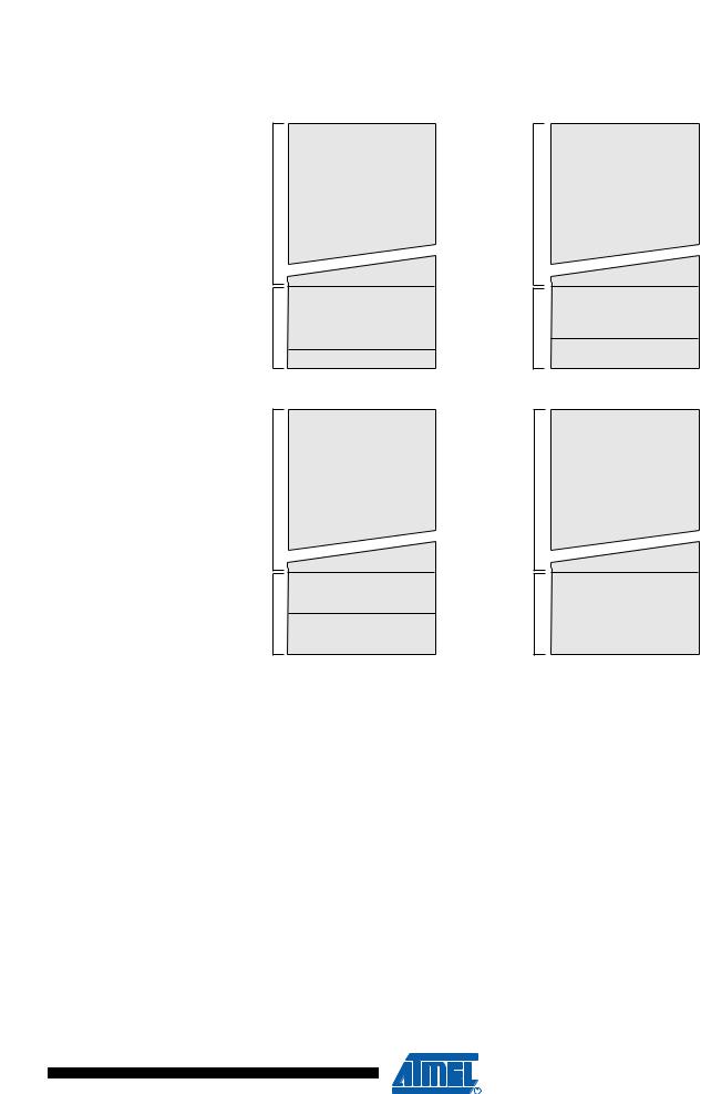
Figure 26-2. Memory Sections
No Read-While-Write Section Read-While-Write Section No Read-While-Write Section Read-While-Write Section
Program Memory
BOOTSZ = '11'
Application Flash Section
Application Flash Section
Boot Loader Flash Section
Program Memory
BOOTSZ = '01'
Application Flash Section
Application Flash Section
Boot Loader Flash Section
0x0000
End RWW
Start NRWW
End Application
Start Boot Loader
Flashend
0x0000
End RWW
Start NRWW
End Application
Start Boot Loader
Flashend
No Read-While-Write Section Read-While-Write Section No Read-While-Write Section Read-While-Write Section
Program Memory
BOOTSZ = '10'
0x0000
Application Flash Section
End RWW
Start NRWW
Application Flash Section
End Application
Start Boot Loader
Boot Loader Flash Section
Flashend
Program Memory
BOOTSZ = '00'
0x0000
Application Flash Section
End RWW, End Application
Start NRWW, Start Boot Loader
Boot Loader Flash Section
Flashend
Note: 1. The parameters in the figure above are given in Table 26-7 on page 283.
26.5Boot Loader Lock Bits
If no Boot Loader capability is needed, the entire Flash is available for application code. The Boot Loader has two separate sets of Boot Lock bits which can be set independently. This gives the user a unique flexibility to select different levels of protection.
The user can select:
•To protect the entire Flash from a software update by the MCU.
•To protect only the Boot Loader Flash section from a software update by the MCU.
•To protect only the Application Flash section from a software update by the MCU.
•Allow software update in the entire Flash.
See Table 26-2 and Table 26-3 for further details. The Boot Lock bits can be set in software and in Serial or Parallel Programming mode, but they can be cleared by a Chip Erase command only. The general Write Lock (Lock Bit mode 2) does not control the programming of the Flash memory by SPM instruction. Similarly, the general Read/Write Lock (Lock Bit mode 1) does not control reading nor writing by LPM/SPM, if it is attempted.
274
8161B–AVR–01/09

 ATmega48PA/88PA
Table 26-2. |
Boot Lock Bit0 Protection Modes (Application Section)(1) |
||||
BLB0 Mode |
|
BLB02 |
BLB01 |
Protection |
|
|
|
|
|
|
|
|
1 |
|
1 |
1 |
No restrictions for SPM or LPM accessing the Application |
|
|
section. |
|||
|
|
|
|
|
|
|
|
|
|
|
|
|
2 |
|
1 |
0 |
SPM is not allowed to write to the Application section. |
|
|
|
|
|
|
|
|
|
|
|
SPM is not allowed to write to the Application section, and LPM |
|
|
|
|
|
executing from the Boot Loader section is not allowed to read |
|
3 |
|
0 |
0 |
from the Application section. If Interrupt Vectors are placed in |
|
|
|
|
|
the Boot Loader section, interrupts are disabled while executing |
|
|
|
|
|
from the Application section. |
|
|
|
|
|
|
|
|
|
|
|
LPM executing from the Boot Loader section is not allowed to |
|
4 |
|
0 |
1 |
read from the Application section. If Interrupt Vectors are placed |
|
|
in the Boot Loader section, interrupts are disabled while |
|||
|
|
|
|
|
|
|
|
|
|
|
executing from the Application section. |
|
|
|
|
|
|
Note: |
1. “1” means unprogrammed, “0” means programmed |
||||
Table 26-3. |
Boot Lock Bit1 Protection Modes (Boot Loader Section)(1) |
||||
BLB1 Mode |
|
BLB12 |
BLB11 |
Protection |
|
|
|
|
|
|
|
|
1 |
|
1 |
1 |
No restrictions for SPM or LPM accessing the Boot Loader |
|
|
section. |
|||
|
|
|
|
|
|
|
|
|
|
|
|
|
2 |
|
1 |
0 |
SPM is not allowed to write to the Boot Loader section. |
|
|
|
|
|
|
|
|
|
|
|
SPM is not allowed to write to the Boot Loader section, and LPM |
|
|
|
|
|
executing from the Application section is not allowed to read |
|
3 |
|
0 |
0 |
from the Boot Loader section. If Interrupt Vectors are placed in |
|
|
|
|
|
the Application section, interrupts are disabled while executing |
|
|
|
|
|
from the Boot Loader section. |
|
|
|
|
|
|
|
|
|
|
|
LPM executing from the Application section is not allowed to |
|
4 |
|
0 |
1 |
read from the Boot Loader section. If Interrupt Vectors are |
|
|
placed in the Application section, interrupts are disabled while |
|||
|
|
|
|
|
|
|
|
|
|
|
executing from the Boot Loader section. |
|
|
|
|
|
|
Note: |
1. “1” means unprogrammed, “0” means programmed |
||||
26.6Entering the Boot Loader Program
Entering the Boot Loader takes place by a jump or call from the application program. This may be initiated by a trigger such as a command received via USART, or SPI interface. Alternatively, the Boot Reset Fuse can be programmed so that the Reset Vector is pointing to the Boot Flash start address after a reset. In this case, the Boot Loader is started after a reset. After the application code is loaded, the program can start executing the application code. Note that the fuses cannot be changed by the MCU itself. This means that once the Boot Reset Fuse is programmed, the Reset Vector will always point to the Boot Loader Reset and the fuse can only be changed through the serial or parallel programming interface.
Table 26-4. |
Boot Reset Fuse(1) |
|
BOOTRST |
|
Reset Address |
|
|
|
1 |
|
Reset Vector = Application Reset (address 0x0000) |
|
|
|
0 |
|
Reset Vector = Boot Loader Reset (see Table 26-7 on page 283) |
|
|
|
Note: 1. “1” means unprogrammed, “0” means programmed
275
8161B–AVR–01/09
 ATmega48PA/88PA
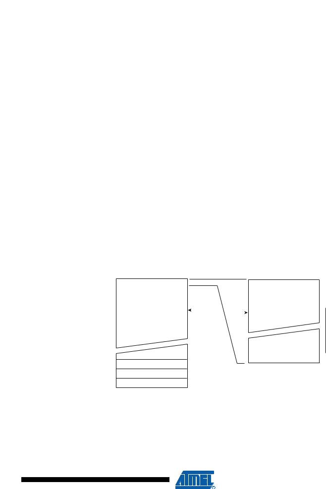
26.7Addressing the Flash During Self-Programming
The Z-pointer is used to address the SPM commands.
Bit |
15 |
14 |
13 |
12 |
11 |
10 |
9 |
8 |
ZH (R31) |
Z15 |
Z14 |
Z13 |
Z12 |
Z11 |
Z10 |
Z9 |
Z8 |
|
|
|
|
|
|
|
|
|
ZL (R30) |
Z7 |
Z6 |
Z5 |
Z4 |
Z3 |
Z2 |
Z1 |
Z0 |
|
|
|
|
|
|
|
|
|
|
7 |
6 |
5 |
4 |
3 |
2 |
1 |
0 |
Since the Flash is organized in pages (see Table 27-8 on page 290), the Program Counter can be treated as having two different sections. One section, consisting of the least significant bits, is addressing the words within a page, while the most significant bits are addressing the pages. This is1 shown in Figure 26-3. Note that the Page Erase and Page Write operations are addressed independently. Therefore it is of major importance that the Boot Loader software addresses the same page in both the Page Erase and Page Write operation. Once a programming operation is initiated, the address is latched and the Z-pointer can be used for other operations.
The only SPM operation that does not use the Z-pointer is Setting the Boot Loader Lock bits. The content of the Z-pointer is ignored and will have no effect on the operation. The LPM instruction does also use the Z-pointer to store the address. Since this instruction addresses the Flash byte-by-byte, also the LSB (bit Z0) of the Z-pointer is used.
Figure 26-3. Addressing the Flash During SPM(1)
BIT 15 |
|
|
|
ZPCMSB |
|
|
|
ZPAGEMSB 1 0 |
|
|||||||||
Z - REGISTER |
|
|
|
|
|
|
|
|
|
|
|
|
0 |
|
|
|
|
|
|
|
|
|
|
|
|
|
|
|
|
|
|
|
|
|
|
|
|
|
PROGRAM |
|
PCMSB |
|
|
|
PAGEMSB |
|
|
|
|
|||||||
|
|
|
PCPAGE |
PCWORD |
|
|
|
|
|
|||||||||
|
COUNTER |
|
|
|
|
|
||||||||||||
|
|
|
|
|
|
|
|
|
|
|
|
|
|
|||||
|
|
|
PAGE ADDRESS |
|
|
WORD ADDRESS |
|
|||||||||||
|
|
|
WITHIN THE FLASH |
|
|
WITHIN A PAGE |
|
|||||||||||
PROGRAM MEMORY |
|
|
|
|
|
|
|
|
|
PAGE |
PCWORD[PAGEMSB:0]: |
|||||||
|
|
|
|
|
|
|
|
|
|
|
|
|
|
|
|
|
|
|
|
PAGE |
|
|
|
|
|
|
|
|
|
|
|
|
INSTRUCTION WORD |
00 |
|||
|
|
|
|
|
|
|
|
|
|
|
|
|
|
|
||||
|
|
|
|
|
|
|
|
|
|
|
|
|
|
|
|
|
|
01 |
|
|
|
|
|
|
|
|
|
|
|
|
|
|
|
|
|
|
|
|
|
|
|
|
|
|
|
|
|
|
|
|
|
|
|
|
|
02 |
|
|
|
|
|
|
|
|
|
|
|
|
|
|
|
|
|
|
|
|
|
|
|
|
|
|
|
|
|
|
|
|
|
|
|
|
|
|
|
|
|
|
|
|
|
|
|
|
|
|
|
|
|
|
|
|
|
|
|
|
|
|
|
|
|
|
|
|
|
|
|
|
|
|
|
|
|
|
|
|
|
|
|
|
|
|
|
|
|
|
|
|
|
|
|
|
|
|
|
|
|
|
|
|
|
|
|
|
|
|
|
|
|
|
|
|
|
|
|
|
|
|
|
|
|
|
|
|
|
|
|
|
|
|
|
|
|
|
|
|
|
|
|
|
|
|
|
|
|
|
|
|
|
|
|
|
|
|
|
|
|
|
|
|
|
|
|
|
|
|
|
|
|
|
|
|
|
|
|
|
|
|
|
|
|
|
|
|
|
|
|
|
|
|
|
|
|
|
|
|
|
|
|
|
|
|
|
|
|
|
|
|
|
|
|
|
|
|
|
|
|
|
|
|
|
|
|
|
|
|
|
|
|
|
|
|
|
|
|
|
|
|
|
|
|
|
|
|
|
|
|
|
|
|
|
|
|
|
|
|
|
|
|
|
|
|
PAGEEND
Note: 1. The different variables used in Figure 26-3 are listed in Table 26-9 on page 283.
26.8Self-Programming the Flash
The program memory is updated in a page by page fashion. Before programming a page with the data stored in the temporary page buffer, the page must be erased. The temporary page buffer is filled one word at a time using SPM and the buffer can be filled either before the Page Erase command or between a Page Erase and a Page Write operation:
276
8161B–AVR–01/09

 ATmega48PA/88PA
Alternative 1, fill the buffer before a Page Erase
•Fill temporary page buffer
•Perform a Page Erase
•Perform a Page Write
Alternative 2, fill the buffer after Page Erase
•Perform a Page Erase
•Fill temporary page buffer
•Perform a Page Write
If only a part of the page needs to be changed, the rest of the page must be stored (for example in the temporary page buffer) before the erase, and then be rewritten. When using alternative 1, the Boot Loader provides an effective Read-Modify-Write feature which allows the user software to first read the page, do the necessary changes, and then write back the modified data. If alternative 2 is used, it is not possible to read the old data while loading since the page is already erased. The temporary page buffer can be accessed in a random sequence. It is essential that the page address used in both the Page Erase and Page Write operation is addressing the same page. See ”Simple Assembly Code Example for a Boot Loader” on page 280 for an assembly code example.
26.8.1Performing Page Erase by SPM
To execute Page Erase, set up the address in the Z-pointer, write “X0000011” to SPMCSR and execute SPM within four clock cycles after writing SPMCSR. The data in R1 and R0 is ignored. The page address must be written to PCPAGE in the Z-register. Other bits in the Z-pointer will be ignored during this operation.
•Page Erase to the RWW section: The NRWW section can be read during the Page Erase.
•Page Erase to the NRWW section: The CPU is halted during the operation.
26.8.2Filling the Temporary Buffer (Page Loading)
To write an instruction word, set up the address in the Z-pointer and data in R1:R0, write “00000001” to SPMCSR and execute SPM within four clock cycles after writing SPMCSR. The content of PCWORD in the Z-register is used to address the data in the temporary buffer. The temporary buffer will auto-erase after a Page Write operation or by writing the RWWSRE bit in SPMCSR. It is also erased after a system reset. Note that it is not possible to write more than one time to each address without erasing the temporary buffer.
If the EEPROM is written in the middle of an SPM Page Load operation, all data loaded will be lost.
26.8.3Performing a Page Write
To execute Page Write, set up the address in the Z-pointer, write “X0000101” to SPMCSR and execute SPM within four clock cycles after writing SPMCSR. The data in R1 and R0 is ignored. The page address must be written to PCPAGE. Other bits in the Z-pointer must be written to zero during this operation.
•Page Write to the RWW section: The NRWW section can be read during the Page Write.
•Page Write to the NRWW section: The CPU is halted during the operation.
277
8161B–AVR–01/09