

Микропроц техника / 4 курс_МТ_МСУД / 8051easy_manual
.pdfm i k r o E l e k t r o n i k a d e v e l o p m e n t s y s t e m s |
|
8051easy |
|
|
|
|
|
|
|
|
|
|
|
|
|
|
development system |
|
|
|
|
|
|
+5V |
|
|
|
|
|
|
|
|
Picture 18. |
|
|
P1.0 |
|
VCC |
|
|
|
|
|
|
|
|
|
||
|
P1.1 |
|
P0.0 |
|
|
|
|
|
|
|
|
|
|
|
|
P1.2 |
|
P0.1 |
|
|
|
|
|
|
|
|
|
|
|
+5V |
P1.3 |
|
P0.2 |
|
|
|
|
|
|
|
|
|
|
|
P1.4 |
|
P0.3 |
|
|
|
|
|
|
|
|
|
|
|
|
|
|
|
|
|
|
|
|
|
|
|
|
|
||
|
P1.5 |
|
P0.4 |
|
|
|
|
|
|
|
|
|
|
|
10K |
P1.6 |
|
P0.5 |
|
|
|
|
|
|
|
|
|
|
|
|
P1.7 |
AT89S8252 |
P0.6 |
|
|
|
|
|
|
|
|
|
|
|
|
RESET |
P0.7 |
|
|
|
|
|
|
|
|
|
|
|
|
|
P3.0 |
ICP |
|
|
|
|
|
|
|
|
|
|
|
|
Reset |
P3.1 |
ALE |
|
|
|
|
|
|
|
|
|
|
|
|
P3.2 |
PSEN |
D7 |
|
|
|
m i K r o e l e k t r o n i k a |
+ |
|||||||
|
P3.3 |
|
P2.7 |
|
|
|
||||||||
|
|
D6 |
|
|
|
|
|
|
|
|
|
|
||
|
P3.4 |
|
P2.6 |
|
|
|
|
|
|
|
|
|
|
|
|
|
D5 |
|
|
|
|
|
|
|
|
|
|
||
|
P3.5 |
|
P2.5 |
|
|
|
|
|
|
|
|
|
|
|
|
|
D4 |
|
|
|
|
|
|
|
|
|
|
||
|
P3.6 |
|
P2.4 |
|
|
|
|
|
|
|
|
|
|
|
|
|
E |
|
|
|
|
|
|
|
|
|
|
||
4MHz |
P3.7 |
|
P2.3 |
|
|
|
|
|
|
|
|
|
|
|
|
RS |
|
|
|
|
|
|
|
|
|
|
|||
|
OSC2/CLKIN |
|
P2.2 |
D7 |
D6 |
D5 |
D4 |
D3 |
D2 |
D1 |
D0 |
E R/W RS Vee Vdd Vss |
|
|
|
|
|
|
|
|
|
|
|
|
1 |
|
|||
|
|
|
|
|
|
|
|
|
|
|
|
|||
|
OSC1/CLKIN |
|
P2.1 |
|
|
|
|
|
|
|
|
|
+5V |
|
|
GND |
|
P2.0 |
|
|
|
|
|
|
|
|
|
|
|
|
|
|
|
|
|
|
|
|
|
|
|
|
KontrastLCD contrastLCD-a |
|
|
1 |
|
|
|
|
|
|
|
|
1 |
|
|
|
|
|
|
|
|
8051 |
|
|
|
|
|
|
|
|
8051 |
|
|
|
|
|
Picture 19. |
|
|
|
|
|
|
|
|
|
Picture 20. |
LCD display connected to port 1. |
LCD display connected to port 2. |
PIC, AVR, MC68HC11, i8051, PSoC development systems www.mikroelektronika.co.yu |
10 |
m i k r o E l e k t r o n i k a d e v e l o p m e n t s y s t e m s |
|
8051easy |
|
|
|
|
|
|
|
|
|
|
|
|
|
|
development system |
|
|
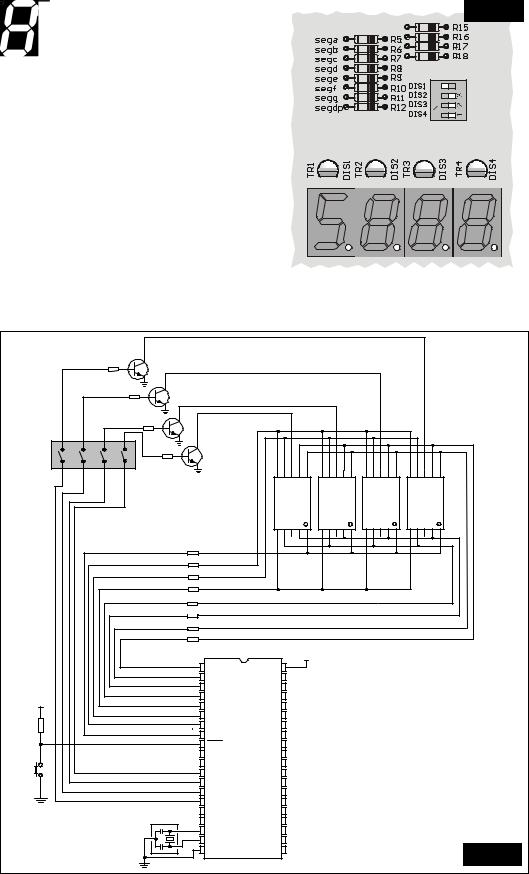
SEVEN-SEGMENT DISPLAYS
Seven-segment display consists of four digits which are refreshed and displayed using port 1 in combination with port 3. Using the DIP switch SW2, you can include or exclude the digits in use. For example, let’s say that we need to enable display of the first digit on the left. By turning the fourth switch (SW2) to (ON), digit of the seven-segment display (DIS1, leftmost digit) will be showing value defined by values of port 1 pins (picture 21.). Procedure is similar with digits DIS2, DIS3 and DIS4. The following picture shows how to connect the seven-segment display to the microcontroller.
Turn on switch Sw2 if you want to use displays
Picture 21.
P3.2
P3.3
P3.4
P3.5
SW2
|
|
|
10ΚΩ |
|
TR4 |
|
|
|
|
|
|
|
|
|
|
|
|
|
|
|
|
|
|
|
|
|
|
10ΚΩ |
TR3 |
|
|
|
|
|
|
|
|
|
|
|
|
|
|
|
|
|
|
|
|
|
|
|
10ΚΩ |
|
|
|
|
|
|
|
|
|
|
|
TR2 |
|
|
|
|
|
|
ON |
|
|
|
|
10ΚΩ |
|
|
|
|
|
|
SW2 |
|
|
|
|
TR1 |
|
|
|
|
|
|
|
|
|
|
|
|
|
|
|
|
||
1 |
2 |
3 |
|
4 |
|
|
|
|
|
|
|
|
|
|
|
|
|
|
|
g f K a b |
g f K a b |
g f K a b |
g f K a b |
|
|
|
|
|
|
|
|
8 8 8 8 |
|||
|
|
|
|
|
|
|
|
e d K c dp |
e d K c dp |
e d K c dp |
e d K c dp |
|
|
|
|
|
330Ω |
h |
|
|
|
|
|
|
|
|
|
|
330Ω |
g |
|
|
|
|
|
|
|
|
|
|
330Ω |
f |
|
|
|
|
|
|
|
|
|
|
330Ω |
e |
|
|
|
|
|
|
|
|
|
|
330Ω |
d |
|
|
|
|
|
|
|
|
|
|
330Ω |
c |
|
|
|
|
|
|
|
|
|
|
330Ω |
b |
|
|
|
|
|
|
|
|
|
|
330Ω |
a |
|
|
|
|
|
|
|
|
|
|
|
|
|
+5V |
|
|
|
|
|
|
|
|
|
P1.0 |
|
VCC |
|
|
|
|
|
|
|
|
|
P1.1 |
|
P0.0 |
|
|
|
|
|
|
|
|
|
P1.2 |
|
P0.1 |
|
|
|
+5V |
|
|
|
|
|
P1.3 |
|
P0.2 |
|
|
|
|
|
|
|
|
P1.4 |
|
P0.3 |
|
|
|
|
|
|
|
|
|
|
|
|
|
|
||
|
|
|
|
|
|
P1.5 |
|
P0.4 |
|
|
|
10K |
|
|
|
|
|
P1.6 |
|
P0.5 |
|
|
|
|
|
|
|
|
|
P1.7 |
AT89S8252 |
P0.6 |
|
|
|
|
|
|
|
|
|
RESET |
P0.7 |
|
|
|
|
|
|
|
|
|
|
P3.0 |
ICP |
|
|
|
|
Reset |
|
|
|
|
|
P3.1 |
ALE |
|
|
|
|
|
|
|
|
|
P3.2 |
PSEN |
|
|
|
||
|
|
|
|
|
|
P3.3 |
|
P2.7 |
|
|
|
|
|
|
|
|
|
P3.4 |
|
P2.6 |
|
|
|
|
|
|
|
|
|
P3.5 |
|
P2.5 |
|
|
|
|
|
|
|
|
|
P3.6 |
|
P2.4 |
|
|
|
|
|
|
|
|
4MHz |
P3.7 |
|
P2.3 |
|
|
|
|
|
|
|
|
|
OSC2/CLKIN |
|
P2.2 |
|
|
|
|
|
|
|
|
|
OSC1/CLKIN |
|
P2.1 |
|
|
|
|
|
|
|
|
|
GND |
|
P2.0 |
|
|
Picture 22. |
|
|
|
|
|
|
|
|
|
|
|
|
PIC, AVR, MC68HC11, i8051, PSoC development systems www.mikroelektronika.co.yu |
11 |

m i k r o E l e k t r o n i k a d e v e l o p m e n t s y s t e m s |
8051easy |
|
ANALOG-DIGITAL CONVERTER
Microcontroller AT89C8252, that can be used in the development system, doesn’t have implemented 10bit A/D coverter. That is why a 12-bit A/D converter LTC1290 is added to the system.
development system
It is possible to read values of
Moguæe je oèitavati
Picture 23. 8 analog inputs vrednosti 8 analognih ulaza
+
+
P1.4
P1.5
P1.6 


If you want to read values of AD0, ..., AD7 inputs, it is neccessary to set the DIP switch SW4 in the position shown on the picture 23. Picture 24. shows how to connect A/D converter and the microcontroller.
|
|
|
|
+5V |
|
|
|
|
|
OE |
Vdd |
|
|
|
|
22μF |
+ |
NC |
NC |
10ΚΩ |
10ΚΩ |
10ΚΩ |
10ΚΩ |
|
NC |
NC |
|||||
|
|
GND |
OUT |
|
|
|
|
|
4 MHZ |
|
|
|
|
1ΚΩ |
CH0 |
Vcc |
|
|
|
|
|
|
|
||
|
CH1 |
ACLK |
|
|
|
+5V |
CH2 |
SCLK |
|
|
|
CH3 |
Din |
|
|
|
|
|
|
|
|
||
|
CH4 |
Dout |
|
|
|
|
CH5 |
CS |
|
|
|
|
CH6 |
REF+ |
|
|
|
|
CH7 |
REF- |
|
|
|
|
COM |
V- |
|
|
|
A/DUlaziconverterA/D |
DGND |
AGND |
|
|
|
|
|
|
|
|
|
konvertorainputs |
LTC1290 |
|
|
|
|
+12V |
NC |
NC |
|
|
|
|
|
|
|
||
|
Vin |
NC |
|
|
|
|
NC |
Vref |
|
|
|
|
GND |
NC |
4.7μF |
+ |
+5V |
|
|
|
|||
|
REF02 |
|
|
||
|
|
|
|
||
|
|
|
|
|
10K |
Reset
4MHz
|
|
|
|
|
|
|
|
Picture 24. |
|
These switches have to be set to |
|
||||||
|
Ovi prekidaèi moraju biti u položaju |
|
||||||
|
|
in order to communicate with |
|
|
||||
|
|
|
||||||
|
ON kako bi se moglo komunicirati sa |
|
|
|||||
|
A/D converter |
|
|
|
|
|||
|
AD konvertorom |
|
|
|||||
|
|
|
|
|
|
|
|
|
CS_AD 4 |
|
|
ON |
|
||||
MOSI |
3 |
|
|
|
|
|
|
|
|
|
|
MISO |
2 |
|
|
|
|
|
|
|
|
|
|
SCK |
1 |
|
|
|
|
|
|
|
|
|
|
|
|
|
|
+5V |
|
|
|
|
|
|
|
P1.0 |
|
|
VCC |
|
|
|
|
|
|
|
|
P1.1 |
|
|
P0.0 |
|
|
|
|
|
|
|
|
P1.2 |
|
|
P0.1 |
|
|
|
|
|
|
|
|
P1.3 |
|
|
P0.2 |
|
|
|
K A n a l : |
5 |
+ |
||
P1.4 |
|
|
P0.3 |
|
|
|
|||||
|
|
|
|
|
|
|
c o n V : |
|
|||
P1.5 |
|
|
P0.4 |
|
|
|
A / d |
|
4 0 9 5 |
||
P1.6 |
|
|
P0.5 |
|
|
|
|
|
|
|
|
P1.7 |
|
AT89S8252 |
P0.6 |
|
|
|
|
|
|
|
|
RESET |
P0.7 |
D7 |
D6 |
D5 |
D4 D3 D2 D1 |
D0 |
E R/W RS Vee Vdd Vss |
|
|||
P3.0 |
|
ICP |
|
|
|
|
|
|
1 |
|
|
P3.1 |
|
ALE |
|
|
|
|
|
|
+5V |
|
|
P3.2 |
|
PSEN |
D7 |
|
|
|
|
|
|
|
|
P3.3 |
|
P2.7 |
|
|
|
|
|
|
KontrastLCD contrastLCD-a |
||
|
|
|
|
|
|
|
|
||||
|
|
D6 |
|
|
|
|
|
|
|||
P3.4 |
|
|
P2.6 |
|
|
|
|
|
|
|
|
|
|
D5 |
|
|
|
|
|
|
|
||
P3.5 |
|
|
P2.5 |
|
|
|
|
|
|
|
|
|
|
D4 |
|
|
|
|
|
|
|
||
P3.6 |
|
|
P2.4 |
|
|
|
|
|
|
|
|
|
|
E |
|
|
|
|
|
|
|
||
P3.7 |
|
|
P2.3 |
|
|
|
|
|
|
|
|
|
|
RS |
|
|
|
|
|
|
|
||
OSC2/CLKIN |
|
P2.2 |
|
|
|
|
|
|
|
||
|
|
|
|
|
|
|
|
|
|||
OSC1/CLKIN |
|
P2.1 |
|
|
|
|
|
|
|
|
|
GND |
|
|
P2.0 |
|
|
|
|
|
|
|
|
PIC, AVR, MC68HC11, i8051, PSoC development systems www.mikroelektronika.co.yu |
12 |

m i k r o E l e k t r o n i k a d e v e l o p m e n t s y s t e m s
RS232 COMMUNICATION
RS232 communication is used for communication between two devices within 10m distance. It is commonly used for data transfer with computer. Jumpers RX and TX select the pin which the communicaton will be attached to.
Picture 26. illustrates the connection between computer and the development system.
Serial connector from the
computer to RS232 commu-
Serijski konektor iz raèunara nicationza RS232 komunikaciju 
If RS232 communication is used,
Ako se koristi RS232 komunikacija jumpers should be set to P3.0
potrebno je postaviti kratkospojnike and P3.1
na P3.0 i P3.1
20 |
MAX232 |
|
18 |
||
|
||
17 |
|
+ |
+ |
+ |
+ |
Tr 6
P3.1 |
P0.3 |
8051easy
development system
Connector for RS232 communication of the microcontroller andKonektorthe computerza RS232(itkomunikacijuis not used
mikrokontrolera i racunara.
for programming the microcon-
(Ne koristi se za programiranje troller)
mikrokontrolera)
Picture 25.
|
|
|
|
|
+5V |
|
+5V |
|
|
+5V |
|
|
|
|
22μF |
|
|
P1.0 |
|
VCC |
|
|
|
|
|
|
|
|
|
|||
|
|
|
C1+ |
Vcc |
|
|
10K |
P1.1 |
|
P0.0 |
|
|
+ |
|
|
P1.2 |
|
P0.1 |
|||
|
F |
|
|
|
|
|
|
|||
|
μ |
|
V+ |
Vss |
|
|
|
|
|
|
|
10 |
|
|
|
|
P1.3 |
|
P0.2 |
||
|
|
|
|
|
|
|
|
|||
|
|
|
|
|
|
|
|
|
||
9 pin SUB-D connector |
|
|
C1- |
T1out |
|
|
Reset |
P1.4 |
|
P0.3 |
SUB-D konektor 9 pinski |
|
|
|
|
|
|
|
|||
|
|
+ |
C2+ |
R1in |
|
|
P1.5 |
|
P0.4 |
|
|
|
|
C2- |
R1out |
|
|
P1.6 |
|
P0.5 |
|
1 |
10Fμ |
|
V- |
16F84T1in |
TX |
P3.1 |
P1.7 |
|
P0.6 |
|
6 |
|
|
||||||||
2 |
22μF |
T2out |
T2in |
|
|
|
RESET |
AT89S8252 |
P0.7 |
|
7 |
|
|
|
|
|
|||||
3 |
|
|
R2in |
R2out |
|
|
|
P3.0 |
ICP |
|
8 |
|
|
|
|
|
|||||
|
|
|
|
RX |
P3.0 |
|
|
|
||
4 |
|
|
MAX232 |
|
P3.1 |
ALE |
||||
9 |
|
|
|
|||||||
|
|
|
|
|
P3.2 |
PSEN |
||||
5 |
|
|
|
|
|
|
|
|||
|
|
|
|
|
|
|
|
P3.3 |
P2.7 |
|
|
|
|
|
|
|
|
|
|
||
|
|
|
|
|
|
|
|
P3.4 |
|
P2.6 |
|
|
|
|
|
|
|
|
P3.5 |
|
P2.5 |
|
|
|
|
|
|
|
|
P3.6 |
|
P2.4 |
|
|
|
|
|
|
|
4MHz |
P3.7 |
|
P2.3 |
|
|
|
|
|
|
|
|
OSC2/CLKIN |
|
P2.2 |
|
|
|
|
|
|
|
|
OSC1/CLKIN |
|
P2.1 |
|
|
|
|
|
|
|
|
GND |
|
P2.0 |
|
serial cable |
|
|
|
|
|
|
|
|
|
|
serijski kabl |
|
|
|
|
|
|
|
|
|
|
|
(1(1naon1)1) |
|
|
|
|
|
|
|
|
1 |
|
|
|
|
|
|
|
|
|
|
6 |
Receives data |
|
|
|
|
|
|
|
||
2 |
prima podatke (Rx) |
|
|
|
|
|
|
|||
7 |
šaljeSendspodatkeata (Tx)(Tx) |
|
|
|
|
|
|
|||
3 |
|
|
|
|
|
|
||||
8 |
|
|
|
|
|
|
|
|
|
|
4 |
|
|
|
|
|
|
|
|
|
|
9 |
|
|
|
|
|
|
|
|
|
|
5 |
|
|
|
|
|
|
|
|
|
|
|
|
|
|
|
|
|
|
|
|
Picture 26. |
PIC, AVR, MC68HC11, i8051, PSoC development systems www.mikroelektronika.co.yu |
13 |

m i k r o E l e k t r o n i k a d e v e l o p m e n t s y s t e m s |
|
8051easy |
|
|
|
|
|
|
|
|
|
|
|
|
|
|
development system |
|
|
DIGITAL TERMOMETER DS1820
DS1820 digital termometer, with temperature range of -55 to 125 C, can be used for measuring enviroment temperature and also for experimenting. It is very accurate and easy to connect. It should be set in the 3-pin socket, beneath the power connector of the development system. Picture 27. shows how to connect digital termometer and the microcontroller on the development system.
|
|
|
|
|
+5V |
|
|
|
|
|
|
|
|
RS |
P1.0 |
|
VCC |
|
|
|
+5V |
DS1820 |
+125 |
|
|
|
P1.1 |
|
P0.0 |
|
|
|
|
|
CO |
|
||
|
|
|
|
|
|
|
|
|
|
|
||
|
E |
P1.2 |
|
P0.1 |
|
|
|
|
Vdd |
DQ GND |
|
|
|
P1.3 |
|
P0.2 |
|
|
|
|
-55 |
|
|||
|
|
|
|
|
|
|
|
|
||||
|
D4 |
|
|
|
|
|
|
|
|
|||
|
P1.4 |
|
P0.3 |
P2.0 |
|
|
|
|
|
|
|
|
|
D5 |
|
|
|
|
|
|
|
|
|||
|
|
|
|
|
|
|
|
|
|
|
||
|
P1.5 |
|
P0.4 |
|
|
|
|
|
|
|
|
|
|
D6 |
|
|
|
|
|
|
|
|
|
||
|
P1.6 |
|
P0.5 |
|
|
|
|
|
|
|
|
|
|
D7 |
|
|
|
|
|
|
|
|
|
||
|
P1.7 |
|
P0.6 |
|
|
|
|
|
|
|
|
|
+5V |
|
AT89S8252 |
P3.6 |
|
|
|
|
4,7ΚΩ |
|
|
||
|
RESET |
P0.7 |
|
|
|
|
|
|
||||
|
|
|
|
|
|
|
|
|
||||
10K |
|
P3.0 |
ICP |
|
|
|
|
|
|
|
||
|
|
P3.1 |
ALE |
|
|
|
|
|
|
|
||
Reset |
|
P3.2 |
PSEN |
|
|
|
|
|
|
|
||
|
P3.3 |
P2.7 |
|
|
|
|
|
|
|
|||
|
|
P3.4 |
|
P2.6 |
|
|
|
|
|
|
|
|
|
|
P3.5 |
|
P2.5 |
|
|
|
|
|
|
|
|
|
|
P3.6 |
|
P2.4 |
|
|
|
|
|
|
|
|
4MHz |
|
P3.7 |
|
P2.3 |
|
|
|
T e m p e r a t u r a |
+ |
|||
|
|
|
|
|
|
|||||||
|
|
OSC2/CLKIN |
|
P2.2 |
|
|
|
2 3 . 5 s t e p e n i c |
|
|||
|
|
OSC1/CLKIN |
|
P2.1 |
|
|
|
|
||||
|
|
|
|
|
|
|
|
|
|
|
||
|
|
GND |
|
P2.0 |
|
|
|
|
|
|
|
|
|
|
|
|
|
D7 |
D6 |
D5 |
D4 D3 D2 |
D1 D0 E |
R/W RS Vee Vdd Vss |
|
|
|
|
|
|
|
|
|
|
|
|
1 |
|
|
|
|
|
|
|
|
|
|
|
|
+5V |
|
|
|
|
|
|
|
|
|
|
|
|
|
LCD contrast |
|
|
|
|
|
|
|
|
|
|
|
|
Kontrast LCD-a |
|
|
|
|
|
|
|
|
|
|
|
|
|
Picture 27. |
Digital temperature value is sent either to P3.6 or P2.0 pin, depending on the position of a jumper, set above DS1820 chip. Half-circle line drawn on the board marks the orientation of DS1820, when setting termometer in the socket.
P3.6
P2.0
Picture 28.
PIC, AVR, MC68HC11, i8051, PSoC development systems www.mikroelektronika.co.yu |
14 |

m i k r o E l e k t r o n i k a d e v e l o p m e n t s y s t e m s |
|
8051easy |
|
|
|
|
|
|
|
|
|
|
|
|
|
|
development system |
|
|
PUL-UP / PULL-DOWN RESISTORS ON PORTS
Setting jumper to the upper position sets the pins of the appropriate port to logical one (pull-up). If jumper is set to the lower postion, pins are set to logical zero (pull-down).
Picture 29. illustrates the situation when the pins of port 0 are predefined to logical one. Graphic schemes are on the following pictures.
Picture 29.
Ω |
5V |
|
|
|
|
Ω |
|
|
|
|
GND |
|
|
||
κ |
|
|
|
|
|
|
κ |
0 |
|
|
|
|
|
|
0 |
0 |
0 |
00κΩ |
0 |
00κΩ |
00κΩ |
00κΩ |
0 |
|
0 |
|
0 |
|
|
|
|
P0.0 |
P0.1 |
P0.2 |
P0.3 |
P0.4 |
P0.5 |
P0.6 |
P0.7 |
|
κ |
|
κ |
|
|
|
|
|
Ω |
|
Ω |
|
|
Picture 30. |
|
DIP system switches enable great flexibility. Through their use, port pins can be connected to various elements of the system:
SW2turn on / turn off seven-segment display digits. SW3turn on / turn off LED diodes on ports 0, 1 ,2 and 3.
SW4pins P1.4, P1.5, P1.6, P1.7 are connected to the appropriate pins of the exernal A/D converter LTC1290 of AVR-easy development sys tem.
PIC, AVR, MC68HC11, i8051, PSoC development systems www.mikroelektronika.co.yu |
15 |

m i k r o E l e k t r o n i k a d e v e l o p m e n t s y s t e m s |
|
8051easy |
|
|
|
|
|
|
|
|
|
|
|
|
|
|
development system |
|
|
DIRECT ACCESS TO PORTS
All PIC pins can be defined as either input or output.
Port pins can be accessed directly from the right side of the development system by using the flat cable. This way, values from external elements can be transferred to ports, both ways.
Picture 32.
PIC, AVR, MC68HC11, i8051, PSoC development systems www.mikroelektronika.co.yu |
16 |