книги / FISMA and the risk management framework the new practice of federal cyber security
..pdf
Evaluating the cohesive strength of a surface material b_,· controlled scratching |
209 |
REFERENCES
1.Dowson, D. (1979). History of Tribology. Longman Group, London.
2. Hawthorne, H.M. and Xie, Y. (1999). Proceedings of the 2"d International Conference on Surface Engineering Wuhan '99, Wuhan, China, pp.18-24.
3.Erickson, L.C., Westergard, R., Wiklund, U., Axen, N., Hawthorne, H.M. and Hogrnark, S. (1998) Wear 214, 30.
4.Xie, Y. and Williams, J.A. (1993) Wear 162-164, 864.
5.Lawn, B.R. (1998) Journal of The American Ceramic Society 81, 1977.
6.Kapoor, A., Johnson, K. L. and Williams, J. A. (1996) Wear 200,38.
7.Williams, J.A. and Xie, Y. (1992) Wear 155, 363.
8.Xie, Y. (1994). Ph.D. Thesis, University of Cambridge, UK.
9.Tabor, D. (1951). Hardness ofmetals. Clarendon Press, Oxford.
10.Johnson, K.L. (1985). Contact mechanics. Cambridge University Press, Cambridge.
II.Xie, Y. and Hawthorne, H.M. (2000) Wear 240, 65.
I2. Xie, Y. and Hawthorne, H.M. (1999) Wear 233-235, 293.
13.Erickson, L. C., Troczynski, T., Ross, D., Tai, H. and Hawthorne, H. M. (I997).
Abstracts ofpapers, the ]51 World Tribology Congress, London, pp. 146.
14.Erickson, L. C., Troczynski, T., Hawthorne, H. M., Tai, H. and Ross, D. (I998).
Proceedings ofthe 151h international Thermal Spray Conference, Nice, pp 79 I-796.
15.Arsenault, B., Legoux, J.G. and Hawthorne, H.M. (1997). In: Thermal Spray: A United Forum for Scientific and Technological Advances, pp. 97-106, Berndt, C.C. (Ed). ASM, Materials Park, Ohio.
16.Yao, M.X., Wu, J.B.C. and Xie, Y. (2005) Materials Science and Engineering: A 407, 234.
17.Hawthorne, H.M. and Xie, Y. (2001) Meccanica 36, 675.
18.Mumm, D.R., Evans, A.G. and Spitsberg, LT. (2001) Acta Materialia 49,2329.
19.Chen, H. and Hutchings, I.M. (1998) Surface and Coatings Technology 101, 106.
20.Wood, R.J.K., Mellor, B.G. and Binfield, M.L. (1997) Wear 211, 70.
21.Hawthorne, H.M., Arsenault, B., Immarigeon, J.P., Legoux, J.G. and Parameswaran, V.R. (1999) Wear 225-229, 825.
22.Marple, B.R., Hawthorne, H.M. and Xie, Y. (2004). Proceedings of2004 International Thermal Spray Conference and Exposition (JTSC 2004), Osaka, Japan.
210
CHAPTER tO
MECHANICAL CHARACTERIZATION OF NANOSTRUCTURED TIB2 COATINGS
USING MICROSCRATCH TECHNIQUES
Originally published in Triho/og1· International vol 39. February 2006
N. PANICH 1•2 andY. SUN3
1School ofMaterials Science and Engineering, Nanyang Technological University, Singapore. 2Metallurgy and Materials Science Research Institute, Chulalongkorn University,
Thailand 10330.
3School ofEngineering & Technology, De Montfort University, Leicester LEI 9BH, UK Email: YSunOJ@dmu.ac.uk
ABSTRACT
TiBz-based nanostructured coatings were fabricated on high-speed steel by magnetron sputtering technique. Mechanical characterization of the resultant coating-substrate systems, such as coating adhesion, friction and scratch resistance, was conducted by microscratch technique. The multi-pass scratch with linearly-increasing load mode of microscratch test was studied to determine the most effective and informative testing conditions and to determine the critical load (Lc) for coating failure. The mode offailure was examined by high resolution SEM and AFM. In order to gain a better understanding of the scratch behaviour during the test, a three-dimensional finite element (FE) model was developed to simulate the scratch process. The developed FE model was able to demonstrate the elastic and plastic behavior of the coating and substrate around the contact area during scratch test. Good agreement has been observed between the FE analysis results and experimental investigations.
KEYWORDS
Microscratch, titanium diboride coating, adhesion, finite element analysis, critical load.
INTRODUCTION
Titanium diboride, TiB2, is well known as a ceramic material with a hexagonal structure which presents various attractive properties, such as high hardness, excellent corrosion, thermal oxidation and wear resistance [1-2]. TiB2 is easy to be deposited by various approaches; one of the most commonly used is magnetron sputtering due to the low cost of operation. Although many attempts have been made to utilize this material as a protective coating, its real and commercial applications have been very limited owing to the difficulties in producing TiB2 coatings with good mechanical integrity [3].
The major problem in producing high quality TiB 2 coatings is that the adhesion of TiB2 coating is poor for the coating-substrate system. Actually, the adhesion of the coating is the most critical
Mechanical characterization of nanostructured Ti82 coatings |
211 |
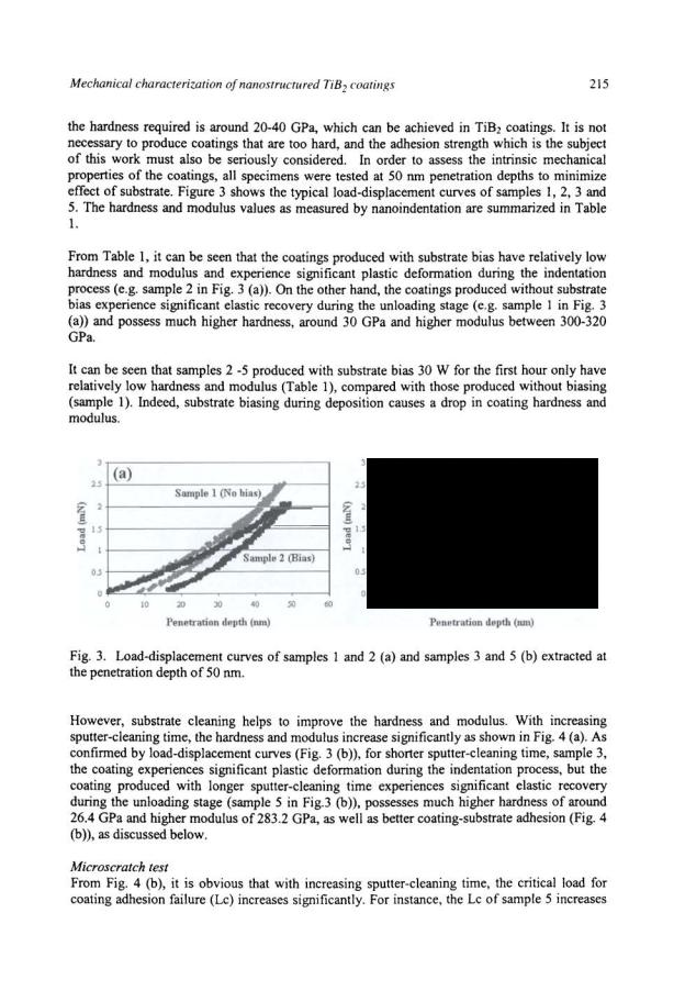
aspect of the coating-substrate system particularly for tribological applications. Recently, Berger et al. [4] developed a method to fabricate TiB2 coatings by d.c. magnetron sputtering by applying a positive substrate bias which could improve the adhesive strength without deteriorating coating hardness, while this could not be done by using negative substrate bias. On the other hand, Panich and Sun [5] addressed that the deposition process can be controlled to produce a TiB2 coating with both high hardness and good adhesion strength. This is achieved by introducing substrate sputter-cleaning and then biasing (rf negative) for the early stage of deposition, followed by deposition without biasing.
In order to determine and analyze the adhesion strength of a coating or thin film to a substrate, scratch test is widely used by research laboratories as well as the industry. In the present work, attempts were made to enhance the adhesion of TiB2-based nanostructured coatings onto highspeed steel substrates with high coating hardness, by applying a small substrate bias and controlling the sputter-cleaning time. This paper discusses further the effect of sputter-cleaning time, with respect to hardness and scratch resistance of the resultant coatings. In order to gain a better understanding of the scratch behaviour during the test, attempts have also been made to simulate the scratch process of the coating-substrate system using the finite element (FE) method. The plastic deformation behaviour indented by a rigid conical indenter has been analyzed to study the elastic-plastic behaviour and the stress-strain of the coating during the scratch process.
EXPERIMENTAL DETAILS
High-speed steel (SECO WKE45, Sweden) in fully hardened and tempered condition was chosen as the substrate in this study. HSS was cut into 12 mm x 12 mm x 3 mm pieces. The specimen's surface was prepared by grinding and polishing and was then ultrasonically cleaned for 10 minutes before charging into the deposition chamber. High-purity argon gas was introduced into the deposited chamber after it was evacuated to below Sx 104 Pa. The Ti target was powered in the direct current (de) mode and TiB2 target was powered in the radio frequency (rt) mode. In order to clean up the targets, the targets were pre-sputtered for 10 minutes with the target shutters closed. The working table where specimens were placed was rotating at 6 rpm during the process. The substrate to target distance was held constant at 10 em for de target (Ti) and at 5 em for rftarget (TiB2). All the experiments were conducted at a constant working pressure of 0.65 Pa and at a total gas flow rate (Ar) of 20 seem. The substrate temperature was 400 oc for all depositions. A rf power biased to the substrate was used before deposition in order to sputter-clean the substrate surface by using a power of !50 W and a rf power of 30 W was also provided to the substrate as bias during the first hour of deposition. The remaining two hours of deposition was conducted without substrate bias. A thin pure Ti interlayer (about 50 nm) was deposited first, by sputtering the Ti target for I 0 minutes with a de power of 200 W. This was followed by sputtering of the TiB2 target for 3 hours with a rfpower of200 W. Process variation was studied with reference to the effect of sputter-cleaning of substrate before deposition as summarized in Table 1. The thickness of the deposited coatings was examined by ball crater, which summarized in Table I.
Nanoindentation test was performed using the NanoTest™ (Micro Materials Limited, UK), with a Berkovich diamond indenter. For the purpose of statistics and reliability, five to ten loading/unloading curves were made in each experiment to find the average results. In the present work, all experiments were performed at a constant loading and unloading rate of 0.1 mN/s and to a maximum depth of 50 nm (controlled depth mode). The hold time at maximum

212 |
Scratching of materials and applications |
load was 30 s, and thermal drift correction was set at 60 s of holding period at 80% unloading. The unloading curves were used to derive the hardness and modulus values by the analytical technique developed by Oliver and Pharr [6].
The microscratch test was performed using the multi-pass microscratch mode available in the NanoTest™ device with a conical diamond indenter (Rockwell type, 120° diamond cone) with spherical tip-end of 25 !lm in radius. A new test method was employed in this work, as described by Xia et. al. [7] and detailed below with reference to Fig. 1.
Tab1e 1 Summaryofdepos1tlon conditions and properties of stud'1ed samples
Materials |
Sputter-cleaning |
|
Substrate |
Coating |
Hardness |
Reduced |
|
Yield load |
|
Critical load |
|||
|
of substrate |
|
bias(W) |
Thickness |
(GPa) |
modulus |
|
Lv (mN) |
|
Lc(mN) |
|||
|
|
|
|
|
|
(nm) |
|
(GPa) |
|
|
|
|
|
Sample I |
No sputter-cleanin~ |
!No bias |
700 |
28.4 |
307.2 |
|
|
98.5 |
353.7 |
||||
Sample2 |
No sputter-cleaning |
|
30 W for the |
650 |
19.2 |
235.5 |
|
|
216.9 |
529.1 |
|||
|
|
|
|
first hour only |
|
|
|
|
|
|
|
|
|
Sample 3 rf 150 W30 min |
|
30 W for the |
650 |
20.8 |
242.5 |
|
276.4 |
595.4 |
|||||
|
|
|
|
first hour only |
|
|
|
|
|
|
|
|
|
Sample4 |
rf 150 W60 min |
|
30 Wfor the |
600 |
23.6 |
275.1 |
|
|
298.3 |
648.5 |
|||
|
|
|
|
first hour only |
|
|
|
|
|
|
|
|
|
Sample 5 |
rf 150 W 90 min |
|
30 W for the |
550 |
26.4 |
2832 |
|
345.8 |
875.5 |
||||
|
|
|
|
first hour only |
|
|
|
|
|
|
|
|
|
|
|
|
|
|
|
|
|
|
|
|
|
|
|
BS: before scratch
DS: during scratch
AS: after scratch
A |
B |
|
|
|
|
|
|
|
|
; |
|
|
|
|
|
|
; |
|
|
|
- - -- |
--~-: |
-----·-·-·---- |
~~-~~::~---- |
·------- |
·-·- |
|
Sliding Distance ().!Inl
Fig. 1. Schematic of the multi-pass microscratch test, showing the before-scratch (BS) profile, the during-scratch (DS) profile, the linearly increasing load during scratch and the after-scratch (AS) profile.
For each test, a set of surface profiles along the track was measured. Firstly, the initial track profile before scratch or surface topography (see BS profile in Fig. 1) was measured by scanning across the full length of distance to be scratched with a small load of 0.25 mN. Then, the scanned length was scratched by applying a linearly increasing load at 5 mN/s after
Mechanical characterization of nanostructured Ti82 coatings |
213 |
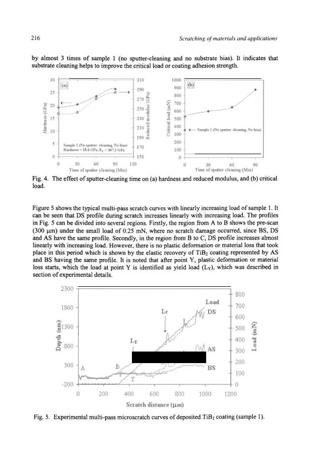
prescanning the initial 300 J..Lm distance under a small initial load of 0.25 mN (from A to B in Fig. I). During scratching, the friction force on the indenter and the surface profile along the full length of the scratched track were measured continually, such that a friction force versus scratching distance (or load) curve and a during-scratch profile (DS profile in Fig. 1) were obtained. The critical load for coating failure (Lc) was determined by the sudden change in friction force, which also led to a sudden change in the DS profile as schematically shown in Fig. I. After the scratch test, a third profile was measured along the full length to obtain an after-scratch profile of the track (AS profile in Fig. I). The difference between BS and DS profiles indicates the total scratch depth including elastic and plastic deformation and surface damage during the scratch process. The difference between BS and AS profiles represents the depth of the scratch groove remaining on the coating surface after the scratch test. Obviously, the difference between AS and DS profiles provides important information on elastic recovery of the coated surface after the scratch test.
The surface profiles obtained from the scratch test outlined above can thus be divided into several regions (Fig. I). Firstly, the region from point A to B is the pre-scan region under a small load of 0.25 mN, where no scratch damage occurred and the three profiles (BS, DS and AS) are the same. In the region from B toY, DS profile increases with increasing load, but there is no plastic deformation or material loss in this region because the scratch depth is fully recovered after the scratch test, as evidenced by the same BS and AS profiles in this region. After point Y, plastic deformation or material loss starts, which leads to continually increased AS profile until point C, at which the DS and AS profiles change suddenly due to the failure of the coating. The load at point Y is hence crucial because it is a maximum scratch load that the coating can sustain without plastic deformation. This critical load is called the "Yield Load (Lv)" [7], and was measured for the TiB2 coatings studied in this work, as listed in Table 1. The critical load at point C (Lc) is a measure of the coating-substrate adhesion strength, as further confirmed by microscopic examination of the scratch track, and was also measured for the coatings studied (Table I).
FINITE ELEMENT MODELLING
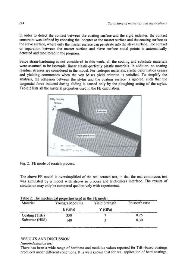
The scratch process was designed as three steps ie. loading (indentation), sliding and unloading. Although scratch process which involves elastic-plastic deformation has been modelled and simulated for bulk materials by the finite element method by some investigators [8-9], very few have modeled the scratch process of coating systems [I 0]. It is recognized that the scratch process in relative motion is a very complex system neither easy to understand nor to predict. In the present study, a three-dimensional (3-D) model has been developed by using the capacities of the ABAQUS finite element (FE) code [II].
The scratch process under consideration involves a hard coating (TiB2) on a substrate (HSS) scratched by a rigid conical indenter. The conical has spherical end form of 25 J..Lm in radius. Accordingly, the scratch process can be modelled with the finite element mesh shown in Fig. 2. A very fine mesh was used in the coating and the substrate adjacent to the contact zone. The mesh was continuously coarsened further away from the contact area. Two element sets, one corresponding to the coating and the other to the substrate, were used to define separately the elastic and plastic properties of the coating and the substrate materials.