

Лабораторная работа 11
Rectifiers
I. Read and memorize the following words:
1.rectifier - выпрямитель
2.to heat - нагревать
3.impurity - примесь
4.hole - дырка
5.charge - заряд
6.polarity - полярность
7.to prevent – препятствовать, мешать
II. Read the following international words and try to guess their meaning:
electric, pneumatic, hydraulic, vacuum, electron, cathode, anode, crystal, nature, cube, atom, positive, dose, percent, material, polarity, metal.
III.Translate the derivatives define to what parts of speech they belong:
1.pure – purity – impurity
2.call – called – calling
3.effect – effective – effectively
4.combine – combination – recombine
5.oppose – opposition – opposite
6.attach – attached – attachment
IV. Match up the antonyms:
a)to heat, purity, positive, to prevent
b)to promote, negative, to cool, impurity
Text A
Rectifiers
A rectifier is an electric check valve. A check valve is a pneumatic or hydraulic device allowing only one-way flow. One-way flow is the key.
An early vacuum tube rectifier was called a Fleming Valve. Electrons would flow from a cathode to an anode but not the other way because the cathode was heated and the anode was not. Vacuum tubes are still called valves in the United Kingdom.
Today’s rectifiers are almost all solid-state based on the PN junction. A PN junction is made of a single crystal (usually silicon) with impurities called “dopants” that change the nature of charge flow in the dopant area. If you put a voltage across a cube of pure silicon, half the current will flow in the form of electrons free of atoms, and half will flow in the form of holes (places where the crystal “thinks” an electron should be). The holes are effectively positive charges. So, if you dose one half the cube with “donor” dopant, 99.9% percent of charge flow becomes electrons, and the material is now called “N”. The other half can be dosed with “acceptor” dopant, and 99.9% of charge flow becomes holes and the material is called “P”. The border is called a PN junction.
46
A PN junction rectifies because only voltage polarity that pushes holes and electrons toward the junction causes current flow. The holes and electrons “recombine” at the junction. The opposite polarity pulling holes and electrons away from the junction, prevents current flow because when the holes come to the attached wire they cannot go further. Metal does not allow “hole flow”.
V.Give English equivalents of the following phrases and words:
электровакуумная лампа; а не наоборот; твердотельный; PN переход; легирующая примесь; чистый кремний; дозировать; граница.
VI. Agree or disagree with the following statements. Use the phrases below: I’m afraid that’s wrong;
you are quite right; you are not quite right; that’s not quite so;
I think you are mistaken; as far as I know; according to the text.
1.A rectifier is an electronic check valve.
2.Vacuum tubes are still called valves in the United Kingdom.
3.Today’s rectifiers are all solid –based on the PN junction.
4.The holes are positive charges.
5.The border is called a PN junction.
VII. Fill in the gaps using the information from the text.
1.A rectifier is … valve.
2.An early vacuum tube rectifier was called a … valve.
3.Electrons would flow from a cathode to an anode but … way.
4.Today’s rectifiers are almost all ….
5.A PN junction is made of … with impurities called ….
6.… are effectively positive charges.
7.The holes and electrons … at the junction.
8.Metal does not allow ….
Text B
I. Read the text:
What is a rectifier and what does it do?
I posted 2 days ago about my tach and volt guage going crazy. One guy said it was probably my rectifier going out. Well, I guess it went ahead and went out. I lost all power this morning to my motor and had to be towed in. Everything went out but troll motor (seperate battery). Bilge, radio, depth finder, aereator, trim, etc, etc, etc all went out. Needless to say the outboard wouldnt crank. What is a rectifier and what exactly does it do? Any explanations on what happened? I'll check back in a few
47
minutes. I'll be outside getting all my fishing stuff out in preparation of taking my rig to the shop. My motor is a 1994 90hp Mariner. Thanks!
II. Answer the questions:
1.What is the source the text was taken from? Explain your answer.
2.What is the problem described in the message?
III. Read these messages and choose the most suitable one for the above mentioned problem. Explain your choice.
(1)10/30/99 4:08:00 PM Submitted by JohnJ (205.188.199.162) from ARKANSAS says rectifier
The rectifier would not shut down all components you described. What a rectifir does is convert the alternating current produced by your alternator to direct current by running the current through its positive and negative diodes. Since an alternator must be energized by current before it will work, the alternator and/or rectifier won't come into play if all accessories have shut down. This sounds more like a tripped breaker, blown fuse to the dash accessories (including key) or a bad ground. The voltmeter and other accessories bouncing sound like a bad ground connection. Check all connection before going to shop. Good luck, John
(2)10/30/99 4:13:00 PM Submitted by k jones (209.124.193.244) from LOUISIANA says bad rectifers your rectifirs charge your starting battery, make your tack work also. look to see if you can see oil are some kind of fluid leaking from them, this is a for sure sign they are gone your starting battery sounds totally dead these arn't hard to change get a shop manual and change them your self, this will save you about an hour's worth of labor at the dealer good luck k jones. they are small black modules by your power packs, yours may be gray being a mariner.
(3)10/30/99 5:15:00 PM Submitted by Spotted Bass (55.30.254.174) from MISSISSIPPI says I'm a DumbAss
Got to looking at my battery and connections. My cables on my ignition battery looked fine upon casual inspection. However after digging on them with my fingernail, I rediscovered/remembered that they are copper. They looked silver. So I scraped them down to the copper real good, re-connected and viola.........back in business just in time for tomorrows fishing. I havent put it back in the water yet to see if that was what was making my tach and volt guage go nuts, but I suspect that it was. Thanks guys for the responses and may you catch a big old lunker tommorrow.
(4)10/30/99 8:20:00 PM Submitted by shipwrek (216.168.96.25) from ALABAMA says rectifiers the 90hp mariner has a stator, rectifier, and a battery, the stator includes the charge for the ingnition and the lighting coil, which produce AC voltatage the 2 yellow wires go to your rectifier/regulator which change the ac voltage to DC through diodes, this has two yellows, one gray, one or two reds., yellows are input to the rectifier, gray is your tach signal(AC) the male red is the sense wire to see if the battery needs a charge, the red female is the DC output to the battery, oh ya black thats ground of course., this must be checked with a multimeter for voltage output with a full load on the battery.. approxl3.75v and if you have a amp meter its good to check the amp output also also.sorry get a book for proper test procedure.,
48
check to see if you have a black stator if you do you may want to save some $$$$$ for it because it will be failing soon if you continue to have battery problems...look under the cowl for your emergency pull cord, the motor will always start even if you have a bad battery, unless you have no spark of course, now thats a mouth full...good luck!!!
(5) 10/30/99 10:11:00 PM Submitted by McCoy (152.163.204.21) from TENNESSEE says Rectifier
Loose battery cables can burn out your rectifier. Changing batteries while the motor is running can burn one out. I learned that the hard way. When my rectifier/regulator went out, the tach would work when the motor was running under 1000 RPMs but would quit at higher speeds and the battery would not change.
IV. Choose the words you want to remember, but not the ones that aren’t worth remembering.
V. Make sentences of your own with these words.
VI. Write your own message in reply.
49
Лабораторная работа 12
Transistors and semiconductors
I. Read and memorize the following words:
1.energy –band gap – запрещенная зона; ширина запрещенной зоны
2.elemental semiconductor – простой полупроводник
3.compound –смесь; соединение
compound semiconductor – сложный полупроводник
4.intrinsic semiconductor – собственный полупроводник
5.extrinsic semiconductor – примесный полупроводник
6.to visualize – мысленно представлять себе; делать видимым, зримым, ощутимым
7.to bind (bound) – связывать, скреплять
8.lattice – кристаллическая решетка
9.adjacent – примыкающий, смежный, соседний
10.conduction band – зона проводимости,
valence band – валентная зона
11.to excite – возбуждать
12.doping – легирование, введение примеси
13.resistivity – удельное сопротивление
14.impurity – примесь
15.ruggedness – прочность, устойчивость
16.radiant – излучающий; лучистый
17.push-pull amplifier – двухтактный усилитель
18.matching transformer – согласующий трансформатор
II. Analyse the following derivatives and find their roots. Give more examples of similar word formation.
Semiconductor, classified, easily, direction, essentially, concentration, revolutionize, ruggedness, small – dimensioned, reliability
III. Make sure that you know the words below. What parts of speech do they belong to and what derivatives can they form?
Conduct, flow, charge, fill, capable, exhibit, pure, modify, gain, design, consume, transform, oscillate, provide, amplify, supply
IV. Match up
1. the synonyms
a)advance, to increase, to contain, motion, to arise from, perfect, to participate, property, fabrication, important
b)movement, indispensable, achievement, to result from, to enlarge, ideal, to comprise, to take part, manufacture, feature
2. the antonyms
50
a)elemental, ability, intrinsic, to bind, solid, opposite, possible, vacant, bulky,
mobile
b)inability, liquid, compound, similar, extrinsic, impossible, still, to disconnect, compact, occupied
V. Look through the following terms and make sure that you remember them. Try to explain the terms and use them in your own sentences and situations:
conductor, semiconductor, insulator, charge carrier, positive charge carrier, negative charge carrier, electrical conduction, vacuum tube, transistor, amplification, current gain, lifetime, reliability, photocell, light source, low-impedance load, lowvoltage device, communications system, noise performance, transmitter.
VI. Read and translate the text.
Transistors and Semiconductors
One of the important advances in the development of electronics is the invention of semiconductor materials, a form of matter situated between metals and insulators in their ability to conduct electricity.
The semiconductor is an electric conductor with resistivity in the range between metals and insulators, in which the electric charge – carrier concentration increases with the increasing temperature range. Semiconductors are usually materials which have energy – band gaps smaller than 2 e V. Semiconductors can be crystalline or amorphous and are classified as elemental and compound, intrinsic and extrinsic semiconductors.
Elemental semiconductors are single-element semiconductor materials such as silicon or germanium. Compound semiconductors are materials containing more that one element, for example, III-V compounds such as gallium, arsenide, aluminium, arsenide, cadmium sulfide and copper oxide.
Unlike the vacuum tube where current flow arises from the motion of charge carriers within a vacuum, semiconductor devices develop current flow from the motion of charge carriers within a crystalline solid. The conduction process in semiconductors is most easily visualized in terms of silicon and germanium which are by far the most widely used semiconducting materials. The atoms of each of these elements have four electrons in the outer shell (valence shell). These electrons are normally bound in the crystalline lattice structure. Some of these valence electrons are free at room temperature, and hence can move through the crystal; the higher the temperature; the more electrons are free to move. Each vacancy, or hole, left in the lattice can be filled by an adjacent valence electron. Since a hole moves in a direction opposite to that of an electron, a hole may be considered as a positive-charge carrier.
Electrical conduction is possible by the motion of electrons or holes. A perfect semiconductor is essentially an insulator at absolute zero temperature, since its conduction band is vacant. As the temperature increases electrons are thermally excited from the valence into the conduction band and the conductivity increases. The
51
free electrons in the conduction band and the holes in the valence band participate in electrical conduction.
The electrons are negative charge carriers, while the holes are positive carriers. An important property of semiconductors is the ability to change their resistivity
over several orders of magnitude by doping. Semiconductors with a low impurity concentration having electrical properties of the pure semiconductor material are called intrinsic semiconductors. Intrinsic semiconductors exhibit a negative coefficient of resistivity, since the number of carriers increases with temperature. Semiconductors with electrical properties modified by impurities are called extrinsic semiconductors. Semiconductor materials are widely used in the fabrication of transistors and diodes.
A transistor is an active semiconductor device with three or more electrodes. It is called active since the transistor is capable of amplification and current, voltage and power gain. A transistor is an electron device in which electronic conduction takes place within a semiconductor.
Transistors revolutionized radioengineering and electronics replacing bulky vacuum tubes and becoming indispensable in many applications. Having small size, great mechanical ruggedness, long lifetime and high reliability, transistors make it possible to design compact, small-dimensioned electronic devices which consume very little power and to produce devices which cannot be made with vacuum tubes.
The transistors are used for direct transformation of heat energy into electrical energy by means of thermal elements. They are also used to transform radiant energy into electricity with the help of photocells or so called solar batteries. In later years light sources and lasers were built on the basis of transistors.
The range of transistor applications is very wide. Transistors are used in class B push-pull amplifiers for high-power linear applications. Since the transistor is a lowvoltage device, low-impedance loads such as speakers and servomotors can be driven without a matching transformer.
High-frequency applications of transistors include amplifiers, oscillators and mixers in communications system. They provide useful power gains with noise performance superior to that of vacuum tubes. High-frequency transistors used in mobile transmitters can supply 50W at 500 MHz.
VII. Find in the text the English equivalents of the following phrases
Способность проводить электричество; концентрация носителей электрического заряда; кристаллические и аморфные полупроводники; полупроводниковые материалы, состоящие из одного элемента; соединения элементов III-V групп; движение носителей заряда внутри кристаллического твердого тела; с точки зрения кремния и германия; структура кристаллической решетки; соседний валентный электрон; принимать участие в электропроводности; способность изменять удельное сопротивление посредством легирования; низкая концентрация примеси; электрические свойства, изменяемые примесями; усиление по току, напряжению и мощности; незаменимые во многих сферах применения; конструировать компактные, малогабаритные электронные устройства; непосредственное преобразование тепловой энергии в электрическую энергию; шумовая характеристика, превосходящая характеристику электровакуумных ламп.
52
VIII. Agree or disagree with the following statements. Correct the wrong statements.
1.The invention of semiconductor materials has negligible importance for the development of electronics.
2.Electronical conduction of the semiconductor increases with the increasing temperature range.
3.Semiconductor materials exit only in one form.
4.Current flow in semiconductor devices results from the motion of charge carriers within a crystalline solid unlike the vacuum tube where current flow depends on the motion of charge carriers within a vacuum.
5.Electrical conduction is possible by the motion of electronics or holes. The electrons are negative charge carriers while the holes are positive ones.
6.Electrical properties of semiconductors can't be modified by impurities.
7.Transistors revolutionized radioengineering and become indispensable in many applications.
8.The range of transistor applications is not wide.
IX. Explain what property determines the classification of materials into conductors, semiconductors and insulations.
X. Dwell on types of semiconductors and their properties.
XI. Describe the mechanism of electrical conduction and its possible forms.
XII. Complete the following diagram to present the important characteristics of semiconductors and transistors.
|
Semiconductor |
|
|
|
Transistor |
|
||||
|
|
|
|
|
|
|
|
|
|
|
|
|
|
|
|
|
|
|
|
|
|
|
|
|
|
|
|
|
|
|
|
Spheres of |
types |
|
|
|
|
|
|
|
|
||
|
properties |
|
structure |
|
|
|||||
|
|
|
|
application |
||||||
|
|
|
|
|
|
|||||
|
|
|
|
|
|
|
|
|
|
|
|
|
|
|
|
|
|
|
|
|
|
advantages
XIII. Speak on semiconductors and transistors, their characteristics, spheres of application and perspectives.
XIV. Read the text and say what is the subject of the text?
53
The point-contact transistor1 was invented in 1948 by John Bardeen and Walter H. Brattain, members of a team at Bell Telephone Laboratories working under the direction of William Shockley. “Invented” may not be the right word: “discovered” may be more correct, and Shockley himself has used the words “creative failure” in connection with the work that led to the device.
The work at Bell Telephone laboratories immediately after World War II was directed towards producing a solid-state amplifier using semiconductor materials. Shockley had predicted from theoretical work that the resistance of a piece of semiconductor material should change when it was subjected to an electric field normal to the current flow. Experiments, however, did not confirm2 this. The prediction was, in fact, true but it was not until 1963 that it was verified3 by the invention of the insulated-gate field-effect transistor4. The failure to observe the expected change in resistance was ascribed5 by Bardeen in 1947 to some surface states6 neutralising the effect of the applied electric field. Further experiments were devised to investigate the surface states of a semiconductor material.
Perhaps the most important function of the point-contact transistor was its demonstration that a practical amplifying device could be made using the flow of charges through a semiconductor material. It provided a verification of the theoretical work on solid-state physics that had precended7 it. Much of the material technology that was to be further developed over the next two decades to enable the many newtypes of solid-state devices to be manufactured was developed from work done for the point-contact transistor on the purification of germanium, the growing of single crystals, doping, and preparing small slices of semiconductor material. In many different ways, the point-contact transistor prepared the way for the success of the junction transistor8. The junction transistor was invented by William Shockley of Bell Telephone laboratories in 1949. The original transistor consisted of a piece of a single crystal of germanium containing two n-type regions separated by a p-type region. The two n-type regions were called the base. The two pn junctions were biased9 in the same way as the emitter and collector wires in the point contact transistor had been.
Today the most widely used technique for transistor fabrication is the diffusion process. Without the development of this technique of junction formation, the rapid growth made in all fields of transistor electronics would have been impossible.
The alloy technique preceded the development of the diffusion process. Alloy transistors10 were among the first types manufactured and are still used, because the process is inexpensive and performance of the devices is good at low frequencies.
The diffusion process has many advantages over the alloy process, i.e., precise11 control of junction areas and layer width, nonuniform-resistivity regions to provide for a variety of electrical characteristics, a variety of geometries to optimize current handling12 and frequency response.13 There are many variations of this process, but it basically involves exposing a semiconductor wafer14 of predetermined resistivity to a gaseous flow of impurities in a furnace15. The gaseous impurity atoms thus diffuse into the semiconductor surface, forming a pn junction.
A modification in the diffusion process which led to the development of integrated circuits, large-scale integration and other advanced technologies in
54
semiconductor devices is the planar process16. The term planar refers to a device in which each of the junctions, emitter-base and collector-base, is brought to a common plane surface.
The significance of the planar process is that the pn junctions are terminated17 and protected beneath a silicon oxide layer. Thus many of the surface problems associated with other types of transistor fabrication techniques, i.e., high leakage currents and poor low-current dc gain, are eliminated.
To improve switching speed, operating frequency, dc characteristics, collector voltage ratings, power dissipation, and reliability, the epitaxial collector was introduced to the planar transistor devices. The epitaxial process provides a means of growing a very thin high-purity single crystal layer of semiconductor material on a very heavily doped crystal wafer of the same type.
The topography and geometry of transistors take many shapes. In power transistors the geometry is chosen to favor current-handling capability, whereas in small-signal transistors, high-speed operation is the design goal.
Notes to the text
1.point-contract transistor – точечный транзистор
2.to confirm – подтверждать
3.to verify – проверять; подтверждать, устанавливать истинность
4.insulated-gate field-effect transistor – полевой транзистор с изолированным затвором
5.to ascribe – приписывать; относить за счет чего-либо
6.surface state – поверхностное состояние
7.to precede – предшествовать
8.junction transistor – плоскостной транзистор
9.to bias – смещать, отклонять
10.alloy transistor – сплавной транзистор
11.precise – точный
12.current handling – управление током
13.frequency response – амплитудно-частотная характеристика
14.semiconductor wafer – полупроводниковая пластина
15.furnace – печь
16.planar process – планарная технология
17.to terminate – завершаться, оканчиваться; ограничивать
XV. Say in what connection the following word combinations and phrases are used in the text. Give their Russian equivalents.
“creative failure”; a solid-state amplifier; to be subjected to an electric field; to investigate the surface states of a semiconductor material; a practical amplifying device; the growing of single crystals; two n-type regions separated by a p-type region; the diffusion process; exposing a semiconductor wafer of predetermined resistivity; a common plane surface; the epitaxial process; to take many shapes.
XVI. Find in the text words with similar meaning to the following words.
55
Under the guidance; to forecast; to be exposed; to justify; to be proved; to watch; to attribute; to work out; to research; show; to give; to forerun; to allow; to be produced; to comprise; manufacture; cheap; characteristics; accurate; breadth; importance; connected with; to be excluded; to be built in; form; objective.
XVII. Suggest a suitable title for the text.
XVIII. Divide the text into logical parts, entitle them and write an outline of the
text.
XIX. Speak on the invention of a transistor and modern techniques of transistor fabrication.
XX. Read the text and speak on the types of impurities.
Impurities can be added to semiconductors to modify their electrical properties. This addition is termed doping. Silicon doped with pentavalent substitutional impurities1 such as phosphorus, arsenic, and antimony will have a higher electron density due to the easily ionized fifth electrons of the impurities. The hole concentration in such a silicon crystal is reduced since the np product remains constant. Dopants2 which increase the electron density are called donors3. Dopant concentration is denoted Np.
The addition of trivalent dopants such as boron, gallium, and indium to silicon will attract electrons and reduce the electron density. Again, since the np product remains constant, the hole density must increase. Dopants which reduce the electron density are called acceptors4. Acceptor concentration is denoted Na.
In an extrinsic (doped) semiconductor the current-carrier type introduced by doping predominates. Donor-doped material is called n-type because the majority of carriers are electrons. The electrons in such semiconductors are the majority carriers, while the holes are the majority carriers. Acceptor-doped materials are called p-type. Here the holes are the majority5 carriers and electrons are the minority carriers.
Resistivity is determined by the concentration of majority carriers.
Lifetime is the average time required for excess minority carriers to recombine with majority carriers. Recombination occurs at “traps” caused by impurities and imperfections in the semiconductor crystal. Semiconductor junctions are formed in material grown as a single continuous crystal to obtain the lattice perfection required, and extreme precautions are taken to ensure exclusion of unwanted impurities during processing. However, in some applications short lifetime is desired, and in such cases gold doping is used to achieve this.
Carrier mobility is the property of a charge carrier which determines its velocity in an electric field. Mobility also determines the velocity of a minority carrier in the diffusion process. High mobility yields a short transit time and good frequency response.
56
Notes to the text
1.substitutional impurities – примесь замещения
2.dopant – легирующая примесь 3.donor – донор, донорная примесь
4.acceptor – акцептор, акцепторная примесь 5.majority carrier – основной носитель заряда 6.minority carrier – неосновной носитель заряда
XXI. Explain the purpose of doping.
XXII. Discuss the difference between donor-doped materials and acceptor-doped materials.
XXIII. Explain the terms lifetime and carrier mobility.
57
Лабораторная работа 13
Amplifiers
I. Read and memorize the following words:
1.gain - приобретать
2.d-c (d.c.) = direct current – постоянный ток
3.common - общий
4.magnitude - величина;
5.a-c (a.c.) = alternative current – переменный ток
6.capacitor - конденсатор
7.scores - десятки
8.value – величина, значение
9.in the wake of – вслед за, непосредственно за
10.corresponding - соответствующий
II. Read the following international words and try to guess their meaning:
electronic, battery, economical, type, base, collector, emitter, popular, voltage, component, pulsation, to pulsate, microamperes, milliamperes, to control.
III. Translate the derivatives define to what parts of speech they belong:
1.amplifier – amplification – to amplify – amplified
2.to operate – operation – operating
3.to conduct – conductor – conductivity – semiconductor
4.to consider – consideration – considerable
5.capacitor – capacitance – capacity
IV. Find the equivalents:
1. advantage |
1. |
считать, рассматривать |
2. capacitor |
2. |
величина |
3. value |
3. |
преимущество |
4. suppose |
4. |
постоянный ток |
5. a.c. |
5. |
работа |
6. operation |
6. |
переменный ток |
7. d.c. |
7. |
конденсатор |
8. consider |
8. |
предполагать |
Text A
Transistor Amplifier
(1) In reсent years transistor amplifiers have gained wide acceptance in all branches of electronics The outstanding advantage of these circuits is that no heater voltage supply is required and that a small, low-current d-c source takes care of all transistor current needs, thus making battery operation quite economical. There are
58
types of semiconductor amplifiers, namely: common-base, common-collector and common-emitter amplifiers. Of these the latter is the most popular.
(2)Consider the operation of such an amplifier. First, let us suppose that there is no input signal. Direct current I is flowing in the base circuit, while direct current II is in the collector. The collector voltage II is of a constant magnitude. The alternating input voltage appearing, its variable component induces pulsation of the base current. The changing base current in its turn makes the collector current pulsate. This induces corresponding pulsations of the collector voltage, which come to the current output via capacitor.
(3)In case a low-voltage transistor is used in the circuit, the alternating base current will be in the order of scores of microamperes, while the alternating collector current will be in the order of milliamperes. Thus a low input current controls a high output current, amplifying the input signal.
(4)Thus, in the absence of the input signal the transistor base and collector carry direct currents, their value being determined by the resistance offered by the circuits. Once, the input signal is applied, the base current starts to change in the wake of the input signal, producing corresponding changes in the collector voltage and current.
I. Переведите словосочетания:
absolute value, peak value, power value, working value, optimum value; shunting capacitor, disk capacitor, vacuum capacitor, variable capacitor; radio-frequency operation, broadband operation, unstable operation.
II. Сгруппируйте данные слова по смыслу:
1. stable |
1. advantage |
2. main |
2. current |
3. important |
3. operation |
4. variable |
4. capacitor |
5. alternating |
5. value |
III. Закончите предложения:
1. The outstanding … of transistor amplifiers is that no heater voltage supply is required. 2. Battery … of transistor amplifier is quite economical. 3. Pulsations of the collector voltage come to the circuit output via … .4. In the absence of the input signal the … of the transistor base and collector currents are determined by the resistance offered by the circuits.
__________________________________________________________
1. values; 2. capacitor; 3. operation; 4. advantage.
IV. Опровергните высказывания:
1. There is only one type of semiconductor amplifiers. 2. In this text the operation of common-base amplifier is considered. 3. A low input current in the amplifier controls a low output current.
59
Text B
Types of Amplifier Distortion
I. Read and memorize the following words:
1.frequency - частота;
2.to avoid - избегать;
3.linearity - линейность;
4.distortion - искажение;
5.range - диапазон;
6.to satisfy the requirements – удовлетворять требованиям;
7.occur – происходить, иметь место, случаться;
8.to clip - ограничивать;
9.feedback – обратная связь;
10.to cause – вызывать, стать причиной.
Types of Amplifier Distortions
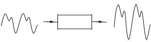
The task of an audio amplifier is to take a small signal and make it bigger without making any other changes in it. This is a demanding task, because a musical sound
Input Amplifier Output
usually contains several frequencies, all of which must be amplified by the same factor to avoid changing the waveform and hence the quality of the sound. An amplifier which amplifies all frequencies and amplitudes by the same factor is said to be linear. Departures from linearity lead to various types of distortions.
Amplifier Distortion.
All frequencies and all amplitudes within an amplifier's operating range must be amplified by the same factor to avoid distortion. An amplifier which satisfies this requirement is said to be perfectly linear. If the peaks of the waveform arc clipped, this gives rise to what is called harmonic distortion. Another type of distortion is intermodulation distortion, which occurs when different frequencies in the signal mix to produce sum and difference frequencies which didn't exist in the signal. Transient distortion occurs when amplifier components cannot handle the rate of change of the signal, for example in rapid percussive attacks. There is also transient intermodulation distortion (TIM) to which modern integrated circuits are susceptible. Such circuits depend upon feedback for their linearity, but time delays in the feedback can cause intermodulation distortion on fast transients in the signal.
60
|
|
|
|
|
|
|
|
Peak |
|
|
Input |
|
Output |
|
|
clipping |
|||
|
Amplifier |
|
|
|
|
||||
|
|
|
|
|
|
|
|
|
|
|
|
|
That frequency |
f |
|
|
|
||
|
|
|
is amplified, but |
|
Harmonic |
||||
|
|
|
|
|
|||||
f |
clipping changes |
|
2 f |
distortion |
|||||
|
Single frequency |
the waveform |
|
|
|
||||
|
and introduces |
|
3 f |
4 f 5 f |
|||||
|
|
||||||||
|
input |
harmonics |
|
|
|||||
|
|
|
|
|
|
|
|||
|
|
|
|
|
|
|
|
|
|
Harmonic Distortion. A common type of amplifier distortion is called harmonic distortion. It can arise if any component in the amplifier clips the peaks of the waveform. A common specification for high fidelity amplifiers is the total harmonic distortion. This distortion may be less than 1%. or even less than 0.5% from 20-20,000 Hz for high quality amplifiers.
Intermodulation Distortion. Non-linearity in amplifier components causes mixing of frequency components to form components at sum and difference frequencies. This intermodulation distortion is particularly troublesome in the reproduction of music because it generates frequencies which were not present in the original music and are thus very noticeable. Harmonic distortion may also be serious, but at least the musical sound probably already had these harmonics present as part of the harmonic content of the sound, so it can be tolerated to a greater degree than intermodulation distortion.
Input |
|
f1 |
Amplified Output |
|
|
|
|
f2 |
|
f1 |
|
|
|
|
f2 |
|
f2 − f1 |
f2 + f1 |
|
|
f2 |
−2 f1 |
f2 +2 f1 |
|
|
|
|||
frequency → |
|
frequency → |
|
|
II. Match the terms in the box with the appropriate definition:
a) cause; |
c) feedback; |
e) frequency. |
|
b) avoid; |
d) range; |
||
|
1.The limits within which something operates, exists or is effective.
2.Uncontrolled noise from an electrical amplification.
3.To keep away from.
4.To lead to.
5.A particular member of radio waves per second at which a radio signal is broadcast.
III. Characterize each type of distortion.
61
Text C
Emtron Amplifiers
I. Translate this text for 30 minutes.
(1)All Emtron amplifiers have been developed with a specific application in mind, and they all have one thing in common - the unique modular construction! All modules except where the power is concerned are interchangeable, irregardless of the model of the amplifier. The advantages of such a construction are enormous - not only from a service point of view, where a few minutes and a screwdriver is all you need. Modular construction also has a big advantage in manufacturing. These "new breed" high quality linear amplifiers are quite unique. Designed and built in Australia by professional engineers, who also happen to be amateur radio operators. At Emtron we sincerely believe that there is no other manually tuned amplifier on the market today that meets the craftsmanship, modern electronic engineering techniques, reliability and features of EMTRON amplifiers.
(2)All Emtron amplifiers have very sophisticated tube protection circuitry, which protects the tube from all possible mishandling. Emtron does not only build amplifiers for amateur service, we also supply custom-built amplifiers for different applications such as professional applications, paramilitary, RF power generators (plasma, industrial and medical applications) as well as broadcasting.
II. Find more information about different types of amplifiers. Be ready to speak about one of them.
62
Учебное издание
Развитие навыков устной речи по специальности «Радиотехника»
Методические указания к лабораторным работам
Составители: Авдейко Светлана Альбертовна Луценко Светлана Александровна Любаева Галина Валентиновна
Корректор Н. С. К у п р и я н о в а
Подписано в печать 08.06.2006 г. Формат 60х84 1/16. Бумага офсетная. Печать офсетная.
Усл. печ. л. 3,7. Усл. кр.-отт. 3,8. Уч.-изд.л. 4,0.
Тираж 200 экз. Заказ . Арт. С-96/2006
Самарский государственный аэрокосмический университет 443086 Самара, Московское шоссе, 34.
_______________________________________________
РИО Самарского государственного аэрокосмического университета.
443086 Самара, Московское шоссе, 34.
63