

 ATtiny13
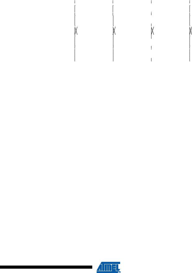
Figure 11-11. Timer/Counter Timing Diagram, Clear Timer on Compare Match mode, with Prescaler (fclk_I/O/8)
clkI/O |
|
|
|
|
|
|
|
|
|
|
|
|
|
|
|
|
|
|
|
|
|
|
|
|
|
|
|
|
|
|
|
|
|
|
|
|
|
|
|
|
|
|
|
|
|
|
|
|
|
|
|
|
|
|
|
|
|
|
|
|
|
|
|
|
|
clkTn |
|
|
|
|
|
|
|
|
|
|
|
|
|
|
|
|
|
|
|
|
|
|
|
|
|
|
|
|
|
|
|
|
|
|
|
|
|
|
|
|
|
|
|
|
|
|
|
|
|
|
|
|
|
|
|
|
|
|
|
|
|
|
|
|
|
|
|
|
|
|
|
|
|
|
|
|
|
|
|
|
|
|
|
|
|
|
|
|
|
|
|
|
|
|
|
|
|
|
|
|
|
|
|
|
|
|
|
|
|
|
|
|
|
|
|
|
|
|
|
|
|
|
|
|
|
|
|
|
|
|
|
|
|
|
|
|
|
|
|
|
|
|
|
|
|
|
|
|
|
|
|
|
|
|
|
|
|
|
|
|
|
|
|
|
|
|
|
|
|
|
|
|
|
|
|
|
|
|
|
|
|
|
|
|
|
|
|
|
|
|
|
|
|
|
|
|
|
(clkI/O/8) |
|
|
|
|
|
|
|
|
|
|
|
|
|
|
|
|
|
|
|
|
|
|
|
|
|
|
|
|
|
|
|
|
|
|
|
|
|
|
|
|
|
|
|
|
|
|
|
|
|
|
|
|
|
|
|
|
|
|
|
|
|
|
|
|
|
TCNTn |
|
|
|
|
|
|
|
|
|
|
|
|
|
|
|
|
|
|
|
|
|
|
|
|
|
|
|
|
|
|
|
|
|
|
|
|
|
|
|
|
|
|
|
|
|
|
|
|
|
|
|
|
|
|
|
|
|
|
|
|
|
|
|
|
|
|
|
|
|
|
|
|
|
TOP - 1 |
|
|
|
|
|
|
|
|
|
|
|
TOP |
|
|
|
|
|
|
|
|
|
|
|
BOTTOM |
|
|
|
|
|
|
|
BOTTOM + 1 |
|
|
|||||||||||||||||||||||
(CTC) |
|
|
|
|
|
|
|
|
|
|
|
|
|
|
|
|
|
|
|
|
|
|
|
|
|
|
|
|
|
|
|
|
|
|
|
|
|
|
|
||||||||||||||||||||||||||
|
|
|
|
|
|
|
|
|
|
|
|
|
|
|
|
|
|
|
|
|
|
|
|
|
|
|
|
|
|
|
|
|
|
|
|
|
|
|
|
|
|
|
|
|
|
|
|
|
|
|
|
|
|
|
|
|
|
|
|
|
|
|
|
||
|
|
|
|
|
|
|
|
|
|
|
|
|
|
|
|
|
|
|
|
|
|
|
|
|
|
|
|
|
|
|
|
|
|
|
|
|
|
|
|
|
|
|
|
|
|
|
|
|
|
|
|
|
|
|
|
|
|
|
|
|
|
|
|
|
|
OCRnx |
|
|
|
|
|
|
|
|
|
|
|
|
|
|
|
|
|
|
|
|
|
|
|
|
|
|
|
|
|
|
|
TOP |
|
|
|
|
|
|
|
|
|
|
|
|
|
|
|
|
|
|
|||||||||||||||
OCFnx |
|
|
|
|
|
|
|
|
|
|
|
|
|
|
|
|
|
|
|
|
|
|
|
|
|
|
|
|
|
|
|
|
|
|
|
|
|
|
|
|
|
|
|
|
|
|
|
|
|
|
|
|
|
|
|
|
|
|
|
|
|
|
|
|
|
|
|
|
|
|
|
|
|
|
|
|
|
|
|
|
|
|
|
|
|
|
|
|
|
|
|
|
|
|
|
|
|
|
|
|
|
|
|
|
|
|
|
|
|
|
|
|
|
|
|
|
|
|
|
|
|
|
|
|
|
|
|
|
|
||
|
|
|
|
|
|
|
|
|
|
|
|
|
|
|
|
|
|
|
|
|
|
|
|
|
|
|
|
|
|
|
|
|
|
|
|
|
|
|
|
|
|
|
|
|
|
|
|
|
|
|
|
|
|
|
|
|
|
|
|
|
|
|
|
||
|
|
|
|
|
|
|
|
|
|
|
|
|
|
|
|
|
|
|
|
|
|
|
|
|
|
|
|
|
|
|
|
|
|
|
|
|
|
|
|
|
|
|
|
|
|
|
|
|
|
|
|
|
|
|
|
|
|
|
|
|
|
|
|
|
|
11.9Register Description
11.9.1TCCR0A – Timer/Counter Control Register A
Bit |
7 |
6 |
5 |
4 |
3 |
2 |
1 |
0 |
|
|
COM0A1 |
COM0A0 |
COM0B1 |
COM0B0 |
– |
– |
WGM01 |
WGM00 |
TCCR0A |
Read/Write |
R/W |
R/W |
R/W |
R/W |
R |
R |
R/W |
R/W |
|
Initial Value |
0 |
0 |
0 |
0 |
0 |
0 |
0 |
0 |
|
• Bits 7:6 – COM01A:0: Compare Match Output A Mode
These bits control the Output Compare pin (OC0A) behavior. If one or both of the COM0A1:0 bits are set, the OC0A output overrides the normal port functionality of the I/O pin it is connected to. However, note that the Data Direction Register (DDR) bit corresponding to the OC0A pin must be set in order to enable the output driver.
When OC0A is connected to the pin, the function of the COM0A1:0 bits depends on the
WGM02:0 bit setting.
Table 11-2 shows the COM0A1:0 bit functionality when the WGM02:0 bits are set to a normal or
CTC mode (non-PWM).
Table 11-2. |
Compare Output Mode, non-PWM Mode |
|
COM01 |
COM00 |
Description |
|
|
|
0 |
0 |
Normal port operation, OC0A disconnected. |
|
|
|
0 |
1 |
Toggle OC0A on Compare Match |
|
|
|
1 |
0 |
Clear OC0A on Compare Match |
|
|
|
1 |
1 |
Set OC0A on Compare Match |
|
|
|
Table 11-3 on page 70 shows the COM0A1:0 bit functionality when the WGM01:0 bits are set to fast PWM mode.
69
2535J–AVR–08/10

|
|
|
|
|
|
|
|
|
|
|
|
|
|
|
|
Table 11-3. |
Compare Output Mode, Fast PWM Mode(1) |
||||||
COM01 |
COM00 |
Description |
|
||||
|
|
|
|
|
|
|
|
0 |
0 |
Normal port operation, OC0A disconnected. |
|
||||
|
|
|
|
|
|
|
|
0 |
1 |
WGM02 = 0: Normal Port Operation, OC0A Disconnected. |
|
||||
WGM02 = 1: Toggle OC0A on Compare Match. |
|
||||||
|
|
|
|||||
|
|
|
|
|
|
|
|
1 |
0 |
Clear OC0A on Compare Match, set OC0A at TOP |
|
||||
|
|
|
|
|
|
|
|
1 |
1 |
Set OC0A on Compare Match, clear OC0A at TOP |
|
||||
|
|
|
|
|
|
|
|
Note: 1. A special case occurs when OCR0A equals TOP and COM0A1 is set. In this case, the Compare Match is ignored, but the set or clear is done at TOP. See “Fast PWM Mode” on page 64 for more details.
Table 11-4 shows the COM0A1:0 bit functionality when the WGM02:0 bits are set to phase correct PWM mode.
Table 11-4. |
|
Compare Output Mode, Phase Correct PWM Mode(1) |
|
COM0A1 |
|
COM0A0 |
Description |
|
|
|
|
0 |
|
0 |
Normal port operation, OC0A disconnected. |
|
|
|
|
0 |
|
1 |
WGM02 = 0: Normal Port Operation, OC0A Disconnected. |
|
WGM02 = 1: Toggle OC0A on Compare Match. |
||
|
|
|
|
1 |
|
0 |
Clear OC0A on Compare Match when up-counting. Set OC0A on |
|
Compare Match when down-counting. |
||
|
|
|
|
|
|
|
|
1 |
|
1 |
Set OC0A on Compare Match when up-counting. Clear OC0A on |
|
Compare Match when down-counting. |
||
|
|
|
|
|
|
|
|
Note: 1. |
A special case occurs when OCR0A equals TOP and COM0A1 is set. In this case, the Com- |
||
|
pare Match is ignored, but the set or clear is done at TOP. See “Phase Correct PWM Mode” on |
||
|
page 66 for more details. |
||
• Bits 5:4 – COM0B1:0: Compare Match Output B Mode
These bits control the Output Compare pin (OC0B) behavior. If one or both of the COM0B1:0 bits are set, the OC0B output overrides the normal port functionality of the I/O pin it is connected to. However, note that the Data Direction Register (DDR) bit corresponding to the OC0B pin must be set in order to enable the output driver.
When OC0B is connected to the pin, the function of the COM0B1:0 bits depends on the
WGM02:0 bit setting.
Table 11-5 on page 71 shows the COM0B1:0 bit functionality when the WGM02:0 bits are set to a normal or CTC mode (non-PWM).
70 ATtiny13 
2535J–AVR–08/10
 ATtiny13
Table 11-5. |
Compare Output Mode, non-PWM Mode |
|
COM01 |
COM00 |
Description |
|
|
|
0 |
0 |
Normal port operation, OC0B disconnected. |
|
|
|
0 |
1 |
Toggle OC0B on Compare Match |
|
|
|
1 |
0 |
Clear OC0B on Compare Match |
|
|
|
1 |
1 |
Set OC0B on Compare Match |
|
|
|
Table 11-6 shows the COM0B1:0 bit functionality when the WGM02:0 bits are set to fast PWM mode.
Table 11-6. |
Compare Output Mode, Fast PWM Mode(1) |
|
COM01 |
COM00 |
Description |
0 |
0 |
Normal port operation, OC0B disconnected. |
|
|
|
0 |
1 |
Reserved |
|
|
|
1 |
0 |
Clear OC0B on Compare Match, set OC0B at TOP |
|
|
|
1 |
1 |
Set OC0B on Compare Match, clear OC0B at TOP |
|
|
|
Note: 1. A special case occurs when OCR0B equals TOP and COM0B1 is set. In this case, the Compare Match is ignored, but the set or clear is done at TOP. See “Fast PWM Mode” on page 64 for more details.
Table 11-7 shows the COM0B1:0 bit functionality when the WGM02:0 bits are set to phase correct PWM mode.
Table 11-7. |
|
Compare Output Mode, Phase Correct PWM Mode(1) |
|
COM0A1 |
|
COM0A0 |
Description |
|
|
|
|
0 |
|
0 |
Normal port operation, OC0B disconnected. |
|
|
|
|
0 |
|
1 |
Reserved |
|
|
|
|
1 |
|
0 |
Clear OC0B on Compare Match when up-counting. Set OC0B on |
|
Compare Match when down-counting. |
||
|
|
|
|
|
|
|
|
1 |
|
1 |
Set OC0B on Compare Match when up-counting. Clear OC0B on |
|
Compare Match when down-counting. |
||
|
|
|
|
Note: 1. |
A special case occurs when OCR0B equals TOP and COM0B1 is set. In this case, the Com- |
||
|
pare Match is ignored, but the set or clear is done at TOP. See “Phase Correct PWM Mode” on |
||
|
page 66 for more details. |
||
• Bits 3, 2 – Res: Reserved Bits
These bits are reserved bits in the ATtiny13 and will always read as zero.
71
2535J–AVR–08/10

• Bits 1:0 – WGM01:0: Waveform Generation Mode
Combined with the WGM02 bit found in the TCCR0B Register, these bits control the counting sequence of the counter, the source for maximum (TOP) counter value, and what type of waveform generation to be used, see Table 11-8 on page 72. Modes of operation supported by the Timer/Counter unit are: Normal mode (counter), Clear Timer on Compare Match (CTC) mode, and two types of Pulse Width Modulation (PWM) modes (see “Modes of Operation” on page 63).
Table 11-8. |
Waveform Generation Mode Bit Description |
|
|
|
|||||
|
|
|
|
|
|
Timer/Counter |
|
|
|
|
|
|
|
|
|
Mode of |
|
Update of |
TOV Flag |
Mode |
|
WGM2 |
WGM1 |
WGM0 |
Operation |
TOP |
OCRx at |
Set on(1)(2) |
|
0 |
|
|
0 |
0 |
0 |
Normal |
0xFF |
Immediate |
MAX |
|
|
|
|
|
|
|
|
|
|
1 |
|
|
0 |
0 |
1 |
PWM |
0xFF |
TOP |
BOTTOM |
|
|
(Phase Correct) |
|||||||
|
|
|
|
|
|
|
|
|
|
|
|
|
|
|
|
|
|
|
|
2 |
|
|
0 |
1 |
0 |
CTC |
OCRA |
Immediate |
MAX |
|
|
|
|
|
|
|
|
|
|
3 |
|
|
0 |
1 |
1 |
Fast PWM |
0xFF |
TOP |
MAX |
|
|
|
|
|
|
|
|
|
|
4 |
|
|
1 |
0 |
0 |
Reserved |
– |
– |
– |
|
|
|
|
|
|
|
|
|
|
5 |
|
|
1 |
0 |
1 |
PWM |
OCRA |
TOP |
BOTTOM |
|
|
(Phase Correct) |
|||||||
|
|
|
|
|
|
|
|
|
|
|
|
|
|
|
|
|
|
|
|
6 |
|
|
1 |
1 |
0 |
Reserved |
– |
– |
– |
|
|
|
|
|
|
|
|
|
|
7 |
|
|
1 |
1 |
1 |
Fast PWM |
OCRA |
TOP |
TOP |
|
|
|
|
|
|
|
|
|
|
Notes: |
1. |
MAX |
= 0xFF |
|
|
|
|
|
|
2.BOTTOM = 0x00
11.9.2TCCR0B – Timer/Counter Control Register B
Bit |
7 |
6 |
5 |
4 |
3 |
2 |
1 |
0 |
|
|
FOC0A |
FOC0B |
– |
– |
WGM02 |
CS02 |
CS01 |
CS00 |
TCCR0B |
Read/Write |
W |
W |
R |
R |
R/W |
R/W |
R/W |
R/W |
|
Initial Value |
0 |
0 |
0 |
0 |
0 |
0 |
0 |
0 |
|
• Bit 7 – FOC0A: Force Output Compare A
The FOC0A bit is only active when the WGM bits specify a non-PWM mode.
However, for ensuring compatibility with future devices, this bit must be set to zero when TCCR0B is written when operating in PWM mode. When writing a logical one to the FOC0A bit, an immediate Compare Match is forced on the Waveform Generation unit. The OC0A output is changed according to its COM0A1:0 bits setting. Note that the FOC0A bit is implemented as a strobe. Therefore it is the value present in the COM0A1:0 bits that determines the effect of the forced compare.
A FOC0A strobe will not generate any interrupt, nor will it clear the timer in CTC mode using
OCR0A as TOP.
The FOC0A bit is always read as zero.
72 ATtiny13 
2535J–AVR–08/10