- •Revision History
- •Table of Contents
- •Introduction
- •Design Strategies
- •Large FPGA Devices
- •SSI Technology
- •Large FPGA Device Methodology
- •Benefits
- •Routing Utilization
- •Consequences of Inefficient Use of Routing Resources
- •Improving Routing Utilization
- •Design Performance
- •Power Consumption
- •Project Costs
- •Stacked Silicon Interconnect (SSI)
- •SSI Components
- •Super Logic Region (SLR)
- •Silicon Interposer
- •Super Long Line (SLL) Routes
- •Master Super Logic Region (SLR)
- •Clocking
- •Regional Clocking
- •Global Clocking (BUFG)
- •Management of Design Placement in SLR Components
- •Automatic SLR Assignment
- •Manual SLR Assignment
- •SSI Hierarchy
- •Achieving High Performance Design in SSI Devices
- •SSI Configuration
- •Configuration Details
- •Partial Reconfiguration
- •System Level Design
- •Pinout Selection
- •Consequences of Pinout Selection
- •Using Xilinx Tools in Pinout Selection
- •General Pinout Selection Recommendations
- •Specific Pinout Selection Recommendations
- •Device Migration
- •Control Sets
- •About Control Sets
- •Resets
- •HDL Coding Styles
- •Inference to Device Resources
- •Choosing Good Design Hierarchy
- •Hierarchical Design
- •Functional and Timing Debugging
- •Pipelining
- •Managing Fanout Non-Clock Nets
- •Clocking
- •Selecting Clocking Resources
- •Global Clocking
- •BUFGCE
- •BUFGMUX
- •BUFGCTRL
- •IP and Synthesis
- •Regional Clocking
- •Horizontal Clock Region Buffers (BUFH, BUFHCE)
- •Regional Clock Buffers (BUFR)
- •I/O Clock Buffers (BUFIO)
- •Multi-Regional Clock Buffers (BUFMR)
- •Clocking for SSI Devices
- •Designs Requiring 16 or Fewer Global Clocks
- •Designs Requiring More Than 16 But Fewer Than 32 Global Clocks
- •Designs Requiring More Than 32 Global Clocks
- •Clock Skew in SSI Devices
- •Multiple Die
- •Specifying the Clocking in the Design
- •Controlling Clock Phase, Frequency, Duty Cycle, and Jitter
- •Using Clock Modifying Blocks
- •Using IDELAY to Control Phase
- •Using Gated Clocks
- •Reducing Dynamic Power
- •Output Clocks
- •Clock Domain Crossings
- •Synchronous Domain Crossings
- •Asynchronous Domain Crossings
- •Controlling and Synchronizing Device Startup
- •Using Clock Buffers for Non-Clock Nets
- •Design Performance
- •Using More Than Two BUFG Components or BUFH Components for Non-Clock Signals
- •Using BUFG Components for Mixed Polarity Signals
- •Using Enables Effectively
- •Buffer Selection
- •Specifying Buffer Placement
- •Clock Resource Selection Summary
- •BUFG
- •BUFGCE
- •BUFGMUX and BUFGCTRL
- •BUFH
- •BUFG
- •BUFHCE
- •BUFR
- •BUFIO
- •BUFMR
- •BUFMRCE
- •MMCM
- •IDELAY and IODELAY
- •ODDR
- •Additional Resources
- •Xilinx Resources
- •Hardware Documentation
- •ISE Documentation
- •Partial Reconfiguration Documentation
- •PlanAhead Documentation
Chapter 3
Stacked Silicon Interconnect (SSI)
This guide addresses all designs targeting large FPGA devices. This chapter discusses designs specifically using the Stacked Silicon Interconnect (SSI) technology.
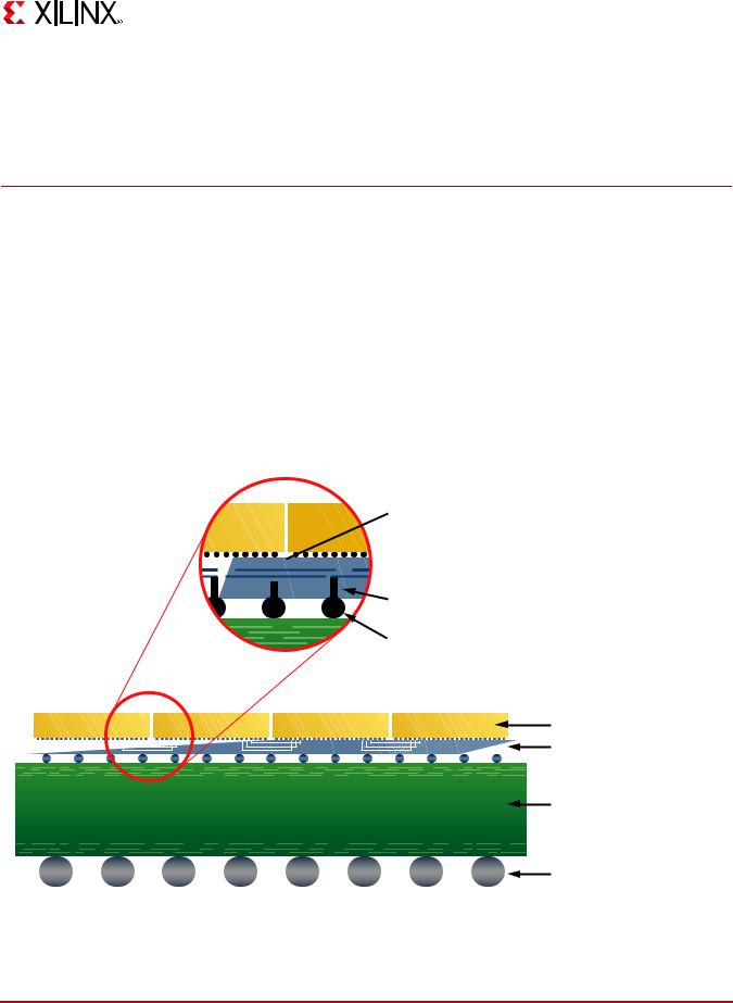
The SSI technology combines multiple Super Logic Region (SLR) components mounted on a passive Silicon Interposer.
Compared to traditional devices, SSI technology enables Xilinx to construct FPGA devices with the following characteristics:
•The devices are much larger.
•The devices have more dedicated features.
•The devices have a lower power envelope.
Note: The terms traditional device and monolithic device refer to devices not using SSI technology.
(IGH "ANDWIDTH N ,OW ,ATENCYT#ONNECTIONS
-ICROBUMPS
4HROUGH 3ILICON 6IAS 436
# "UMPS
3,2 |
3,2 |
3,2 |
3,2 |
&0'! $IE 3,2 |
|
|
|
|
3ILICONI)NTERPOSER |
|
|
|
|
0ACKAGE 3UBSTRATE |
|
|
|
|
"'!'3OLDER "ALLS |
Figure 3-1: Representative SSI Device Construction
Large FPGA Methodology Guide |
www.xilinx.com |
11 |
UG872 (v14.3) October 16, 2012