

Philips Semiconductors |
Product specification |
|
|
|
|
N-channel TrenchMOS™ transistor |
IRF540, IRF540S |
|
|
|
|
FEATURES |
SYMBOL |
|
|
QUICK REFERENCE DATA |
• 'Trench' technology |
|
d |
|
VDSS = 100 V |
• Low on-state resistance |
|
|
|
|
• Fast switching |
|
|
|
ID = 23 A |
• Low thermal resistance |
|
|
|
|
|
|
g |
|
RDS(ON) ≤ 77 mΩ |
|
|
|
|
|
|
|
s |
|
|
|
|
|
|
|
GENERAL DESCRIPTION
N-channel enhancement mode field-effect power transistor in a plastic envelope using 'trench' technology.
Applications:-
•d.c. to d.c. converters
•switched mode power supplies
•T.V. and computer monitor power supplies
The IRF540 is supplied in the SOT78 (TO220AB) conventional leaded package.
The IRF540S is supplied in the SOT404 (D2PAK) surface mounting package.
PINNING |
SOT78 (TO220AB) |
SOT404 (D2PAK) |
PIN DESCRIPTION
tab
1gate
2drain1
3source tab drain
1 2 3
|
tab |
|
2 |
1 |
3 |
LIMITING VALUES
Limiting values in accordance with the Absolute Maximum System (IEC 134)
SYMBOL |
PARAMETER |
CONDITIONS |
MIN. |
MAX. |
UNIT |
|
|
|
|
|
|
VDSS |
Drain-source voltage |
Tj = 25 ˚C to 175˚C |
- |
100 |
V |
VDGR |
Drain-gate voltage |
Tj = 25 ˚C to 175˚C; RGS = 20 kΩ |
- |
100 |
V |
VGS |
Gate-source voltage |
|
- |
± 20 |
V |
ID |
Continuous drain current |
Tmb = 25 ˚C; VGS = 10 V |
- |
23 |
A |
|
|
Tmb = 100 ˚C; VGS = 10 V |
- |
16 |
A |
IDM |
Pulsed drain current |
Tmb = 25 ˚C |
- |
92 |
A |
PD |
Total power dissipation |
Tmb = 25 ˚C |
- |
100 |
W |
Tj, Tstg |
Operating junction and |
|
- 55 |
175 |
˚C |
|
storage temperature |
|
|
|
|
1 It is not possible to make connection to pin:2 of the SOT404 package
August 1999 |
1 |
Rev 1.100 |
Philips Semiconductors |
Product specification |
|
|
N-channel TrenchMOS™ transistor |
IRF540, IRF540S |
|
|
AVALANCHE ENERGY LIMITING VALUES
Limiting values in accordance with the Absolute Maximum System (IEC 134)
SYMBOL |
PARAMETER |
CONDITIONS |
MIN. |
MAX. |
UNIT |
|
|
|
|
|
|
EAS |
Non-repetitive avalanche |
Unclamped inductive load, IAS = 10 A; |
- |
230 |
mJ |
|
energy |
tp = 350 μs; Tj prior to avalanche = 25˚C; |
|
|
|
|
|
VDD ≤ 25 V; RGS = 50 Ω; VGS = 10 V; refer |
|
|
|
IAS |
Peak non-repetitive |
to fig:14 |
- |
23 |
A |
|
|||||
|
avalanche current |
|
|
|
|
|
|
|
|
|
|
THERMAL RESISTANCES
SYMBOL |
PARAMETER |
CONDITIONS |
MIN. |
TYP. |
MAX. |
UNIT |
|
|
|
|
|
|
|
Rth j-mb |
Thermal resistance junction |
|
- |
- |
1.5 |
K/W |
|
to mounting base |
|
|
|
|
|
Rth j-a |
Thermal resistance junction |
SOT78 package, in free air |
- |
60 |
- |
K/W |
|
to ambient |
SOT404 package, pcb mounted, minimum |
- |
50 |
- |
K/W |
|
|
footprint |
|
|
|
|
|
|
|
|
|
|
|
ELECTRICAL CHARACTERISTICS
Tj= 25˚C |
unless otherwise specified |
|
|
|
|
|
|
|
SYMBOL |
PARAMETER |
CONDITIONS |
|
MIN. |
TYP. |
MAX. |
UNIT |
|
|
|
|
|
|
|
|
|
|
V(BR)DSS |
|
Drain-source breakdown |
VGS = 0 V; ID = 0.25 mA; |
|
100 |
- |
- |
V |
|
|
voltage |
Tj = -55˚C |
89 |
- |
- |
V |
|
VGS(TO) |
|
Gate threshold voltage |
VDS = VGS; ID = 1 mA |
|
2 |
3 |
4 |
V |
|
|
|
Tj |
= 175˚C |
1 |
- |
- |
V |
|
|
|
Tj = -55˚C |
- |
- |
6 |
V |
|
RDS(ON) |
|
Drain-source on-state |
VGS = 10 V; ID = 17 A |
|
- |
49 |
77 |
mΩ |
gfs |
|
resistance |
Tj |
= 175˚C |
- |
132 |
193 |
mΩ |
|
Forward transconductance |
VDS = 25 V; ID = 17 A |
|
8.7 |
15.5 |
- |
S |
|
IGSS |
|
Gate source leakage current |
VGS = ± 20 V; VDS = 0 V |
|
- |
10 |
100 |
nA |
IDSS |
|
Zero gate voltage drain |
VDS = 100 V; VGS = 0 V |
|
- |
0.05 |
10 |
μA |
|
|
current |
VDS = 80 V; VGS = 0 V; Tj = 175˚C |
|
- |
- |
250 |
μA |
Qg(tot) |
|
Total gate charge |
ID = 17 A; VDD = 80 V; VGS = 10 V |
|
- |
- |
65 |
nC |
Qgs |
|
Gate-source charge |
|
|
- |
- |
10 |
nC |
Qgd |
|
Gate-drain (Miller) charge |
|
|
- |
- |
29 |
nC |
td on |
|
Turn-on delay time |
VDD = 50 V; RD = 2.2 Ω; |
|
- |
8 |
- |
ns |
tr |
|
Turn-on rise time |
VGS = 10 V; RG = 5.6 Ω |
|
- |
39 |
- |
ns |
td off |
|
Turn-off delay time |
Resistive load |
|
- |
26 |
- |
ns |
tf |
|
Turn-off fall time |
|
|
- |
24 |
- |
ns |
Ld |
|
Internal drain inductance |
Measured tab to centre of die |
|
- |
3.5 |
- |
nH |
Ld |
|
Internal drain inductance |
Measured from drain lead to centre of die |
- |
4.5 |
- |
nH |
|
|
|
|
(SOT78 package only) |
|
|
|
|
|
Ls |
|
Internal source inductance |
Measured from source lead to source |
- |
7.5 |
- |
nH |
|
|
|
|
bond pad |
|
|
|
|
|
|
|
|
|
|
|
|
|
|
Ciss |
|
Input capacitance |
VGS = 0 V; VDS = 25 V; f = 1 MHz |
|
- |
890 |
1187 |
pF |
Coss |
|
Output capacitance |
|
|
- |
139 |
167 |
pF |
Crss |
|
Feedback capacitance |
|
|
- |
83 |
109 |
pF |
August 1999 |
2 |
Rev 1.100 |
Philips Semiconductors |
Product specification |
|
|
N-channel TrenchMOS™ transistor |
IRF540, IRF540S |
|
|
REVERSE DIODE LIMITING VALUES AND CHARACTERISTICS
Tj = 25˚C unless otherwise specified
SYMBOL |
PARAMETER |
CONDITIONS |
MIN. |
TYP. |
MAX. |
UNIT |
|
|
|
|
|
|
|
|
|
IS |
Continuous source current |
|
|
- |
- |
23 |
A |
|
(body diode) |
|
|
|
|
|
|
ISM |
Pulsed source current (body |
|
|
- |
- |
92 |
A |
|
diode) |
|
|
|
|
|
|
VSD |
Diode forward voltage |
IF = 28 |
A; VGS = 0 V |
- |
0.94 |
1.5 |
V |
trr |
Reverse recovery time |
IF = 17 |
A; -dIF/dt = 100 A/μs; |
- |
61 |
- |
ns |
Qrr |
Reverse recovery charge |
VGS = 0 V; VR = 25 V |
- |
200 |
- |
nC |
|
August 1999 |
3 |
Rev 1.100 |
Philips Semiconductors |
Product specification |
|
|
N-channel TrenchMOS™ transistor |
IRF540, IRF540S |
|
|
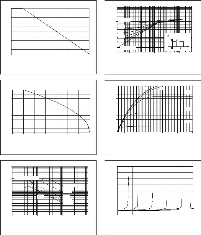
Normalised Power Derating, PD (%)
100
90
80
70
60
50
40
30
20
10
0
0 |
25 |
50 |
75 |
100 |
125 |
150 |
175 |
|
|
Mounting Base temperature, Tmb (C) |
|
|
|||
|
Fig.1. |
Normalised power dissipation. |
|
||||
|
PD% = 100×PD/PD 25 ˚C = f(Tmb) |
|
|
||||
Normalised Current Derating, ID (%) |
|
|
|
||||
100 |
|
|
|
|
|
|
|
90 |
|
|
|
|
|
|
|
80 |
|
|
|
|
|
|
|
70 |
|
|
|
|
|
|
|
60 |
|
|
|
|
|
|
|
50 |
|
|
|
|
|
|
|
40 |
|
|
|
|
|
|
|
30 |
|
|
|
|
|
|
|
20 |
|
|
|
|
|
|
|
10 |
|
|
|
|
|
|
|
0 |
|
|
|
|
|
|
|
0 |
25 |
50 |
75 |
100 |
125 |
150 |
175 |
|
|
Mounting Base temperature, Tmb (C) |
|
|
|||
Fig.2. Normalised continuous drain current. |
|
||||||
ID% = 100×ID/ID 25 ˚C = f(Tmb); conditions: VGS ³ 10 V |
|||||||
1000 |
Peak Pulsed Drain Current, IDM (A) |
|
|
|
|
100 |
RDS(on) = VDS/ ID |
|
|
|
|
|
|
tp = 10 us |
10 |
|
100 us |
|
D.C. |
1 ms |
|
|
10 ms |
1 |
|
100 ms |
0.1 |
|
|
1 |
10 |
100 |
1000 |
|
Drain-Source Voltage, VDS (V) |
|
|
Fig.3. |
Safe operating area. Tmb = 25 ˚C |
|
|
ID & IDM = f(VDS); IDM single pulse; parameter tp
Transient thermal impedance, Zth j-mb (K/W)
10
1 |
D = 0.5 |
|
|
|
|
|
|
|
|
|
|
|
|
|
|
|
|
|
|
|
|
|
|
|
0.2 |
|
|
|
|
|
|
|
|
|
|
|
0.1 |
|
|
|
|
P |
|
|
D = tp/T |
||
0.1 |
0.05 |
|
|
|
|
|
tp |
||||
|
|
|
|
D |
|
|
|
|
|||
|
0.02 |
|
|
|
|
|
|
|
|
|
|
|
single pulse |
|
|
|
|
|
T |
|
|
||
0.01 |
|
|
|
|
|
|
|
|
|
|
|
1E-06 |
1E-05 |
1E-04 |
1E-03 1E-02 |
|
1E-01 |
1E+00 |
|||||
|
|
|
|
Pulse width, tp (s) |
|
|
|
|
|
||
|
Fig.4. Transient thermal impedance. |
|
|||||||||
|
|
Zth j-mb = f(t); parameter D = tp/T |
|
|
|||||||
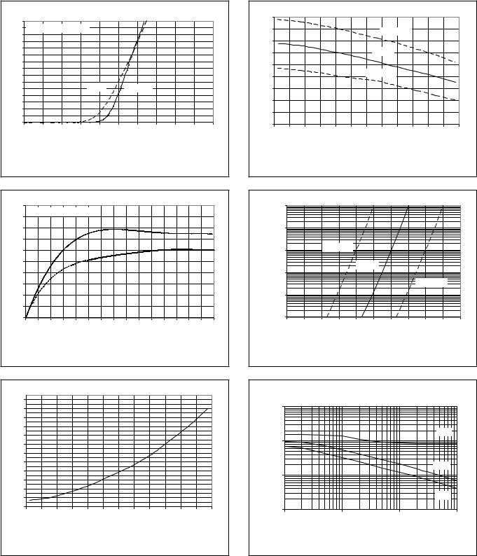
55 |
Drain Current, ID (A) |
|
|
|
|
|
|
|
|
||
|
|
|
9 V |
|
8 V |
|
|
|
|
|
|
50 |
|
|
|
|
|
|
|
|
|
||
|
|
|
|
|
|
|
|
|
|
7 V |
|
45 |
|
|
|
|
|
|
|
|
|
|
|
|
|
|
|
|
|
|
|
|
|
|
|
40 |
|
|
|
|
|
|
|
|
|
|
|
35 |
|
|
|
|
|
|
|
|
|
|
|
30 |
|
|
|
|
|
|
|
|
|
|
6 V |
25 |
|
|
|
|
|
|
|
|
|
|
|
|
|
|
|
|
|
|
|
|
|
|
|
20 |
|
|
|
|
|
|
|
|
|
|
|
15 |
|
|
|
|
|
|
|
|
|
|
5 V |
10 |
|
|
|
|
|
|
|
|
|
|
|
|
|
|
|
|
|
|
|
|
|
|
|
5 |
|
|
|
|
|
|
|
|
|
|
4V |
0 |
|
|
|
|
|
|
|
|
|
|
|
0 |
1 |
2 |
3 |
4 |
5 |
6 |
7 |
|
8 |
9 |
10 |
|
|
|
Drain-Source Voltage, VDS (V) |
|
|
|
|
||||
Fig.5. Typical output characteristics, Tj |
= 25 ˚C. |
||||||||||
|
|
|
|
ID = f(VDS) |
|
|
|
|
|
||
Drain-Source On Resistance, RDS(on) (Ohms)
0.8 |
|
|
|
|
|
0.7 |
|
|
|
|
|
0.6 |
|
|
|
|
|
0.5 |
|
|
|
|
|
0.4 |
4V |
|
|
|
|
5.5V |
|
|
|
|
|
|
|
|
|
|
|
0.3 |
|
6V |
6.5V |
|
|
0.2 |
5 V |
|
7 V |
|
|
|
|
|
|
||
|
|
|
8V |
|
|
|
|
|
|
|
|
0.1 |
|
|
|
|
|
0 |
|
|
|
VGS =9 V |
|
|
|
|
|
|
|
0 |
10 |
20 |
30 |
40 |
50 |
|
|
Drain Current, ID (A) |
|
|
|
Fig.6. Typical on-state resistance, Tj = 25 ˚C.
RDS(ON) = f(ID)
August 1999 |
4 |
Rev 1.100 |
Philips Semiconductors |
Product specification |
|
|
N-channel TrenchMOS™ transistor |
IRF540, IRF540S |
|
|
Drain current, ID (A)
30 |
|
|
|
|
|
|
|
|
|
|
28 |
VDS > ID X RDS(ON) |
|
|
|
|
|
|
|
||
26 |
|
|
|
|
|
|
|
|
|
|
24 |
|
|
|
|
|
|
|
|
|
|
22 |
|
|
|
|
|
|
|
|
|
|
20 |
|
|
|
|
|
|
|
|
|
|
18 |
|
|
|
|
|
|
|
|
|
|
16 |
|
|
|
|
|
|
|
|
|
|
14 |
|
|
|
|
|
|
|
|
|
|
12 |
|
|
|
175 C |
|
Tj = 25 C |
|
|
|
|
10 |
|
|
|
|
|
|
|
|
||
8 |
|
|
|
|
|
|
|
|
|
|
6 |
|
|
|
|
|
|
|
|
|
|
4 |
|
|
|
|
|
|
|
|
|
|
2 |
|
|
|
|
|
|
|
|
|
|
0 |
|
|
|
|
|
|
|
|
|
|
0 |
1 |
2 |
3 |
4 |
5 |
6 |
7 |
8 |
9 |
10 |
|
|
|
Gate-source voltage, VGS (V) |
|
|
|
||||
Fig.7. Typical transfer characteristics. ID = f(VGS)
Threshold Voltage, VGS(TO) (V)
4.5 |
|
|
|
|
|
|
|
|
|
|
|
4 |
|
|
|
|
|
|
maximum |
|
|
|
|
|
|
|
|
|
|
|
|
|
|
||
3.5 |
|
|
|
|
|
|
|
|
|
|
|
3 |
|
|
|
|
|
|
typical |
|
|
|
|
2.5 |
|
|
|
|
|
|
|
|
|
|
|
2 |
|
|
|
|
|
minimum |
|
|
|
||
|
|
|
|
|
|
|
|
|
|
|
|
1.5 |
|
|
|
|
|
|
|
|
|
|
|
1 |
|
|
|
|
|
|
|
|
|
|
|
0.5 |
|
|
|
|
|
|
|
|
|
|
|
0 |
|
|
|
|
|
|
|
|
|
|
|
-60 |
-40 |
-20 |
0 |
20 |
40 |
60 |
80 |
100 120 |
140 |
160 |
180 |
|
|
|
|
Junction Temperature, Tj (C) |
|
|
|
||||
Fig.10. Gate threshold voltage. VGS(TO) = f(Tj); conditions: ID = 1 mA; VDS = VGS
Transconductance, gfs (S) |
|
1.0E-01 |
Drain current, ID (A) |
20 |
|
|
|
VDS > ID X RDS(ON) |
|
|
|
18 |
|
|
|
16 |
Tj = 25 C |
1.0E-02 |
|
|
|
||
14 |
|
175 C |
|
|
|
minimum |
|
12 |
|
1.0E-03 |
|
|
|
10 |
|
|
|
|
|
|
|
|
|
|
|
|
|
|
|
|
|
|
|
typical |
|
|
|
|
|
|
|
|
|
|
|
|
|
|
|
|
|
|
|
|
|
|
|
|
|
|
|
|
|
|
|
||
8 |
|
|
|
|
|
|
|
|
|
|
|
|
|
|
|
1.0E-04 |
|
|
|
|
|
|
|
|
|
|
6 |
|
|
|
|
|
|
|
|
|
|
|
|
|
|
|
|
|
|
|
|
|
|
|
maximum |
|
|
4 |
|
|
|
|
|
|
|
|
|
|
|
|
|
|
|
1.0E-05 |
|
|
|
|
|
|
|
|
|
|
2 |
|
|
|
|
|
|
|
|
|
|
|
|
|
|
|
|
|
|
|
|
|
|
|
|
|
|
0 |
|
|
|
|
|
|
|
|
|
|
|
|
|
|
|
1.0E-06 |
|
|
|
|
|
|
|
|
|
|
0 |
2 |
4 |
6 |
8 |
10 |
12 |
14 |
16 |
18 |
20 |
22 |
24 |
26 |
28 |
30 |
0 |
0.5 |
1 |
1.5 |
2 |
2.5 |
3 |
3.5 |
4 |
4.5 |
5 |
|
|
|
|
|
Drain current, ID (A) |
|
|
|
|
|
|
|
Gate-source voltage, VGS (V) |
|
|
|
||||||||||
Fig.8. |
|
Typical transconductance, Tj = 25 ˚C. |
|
Fig.11. |
Sub-threshold drain current. |
|
|
|||||||||||||||||||
|
|
|
|
|
|
gfs = f(ID) |
|
|
|
|
|
|
|
ID = f(VGS); conditions: Tj = 25 ˚C; VDS = VGS |
|
|||||||||||
Normalised On-state Resistance
2.9 |
|
|
|
|
|
|
|
|
2.7 |
|
|
|
|
|
|
|
|
2.5 |
|
|
|
|
|
|
|
|
2.3 |
|
|
|
|
|
|
|
|
2.1 |
|
|
|
|
|
|
|
|
1.9 |
|
|
|
|
|
|
|
|
1.7 |
|
|
|
|
|
|
|
|
1.5 |
|
|
|
|
|
|
|
|
1.3 |
|
|
|
|
|
|
|
|
1.1 |
|
|
|
|
|
|
|
|
0.9 |
|
|
|
|
|
|
|
|
0.7 |
|
|
|
|
|
|
|
|
0.5 |
|
|
|
|
|
|
|
|
-60 |
-40 |
-20 |
0 |
20 40 60 80 100 |
120 |
140 |
160 |
180 |
|
|
|
Junction temperature, Tj (C) |
|
|
|
|
|
Fig.9. Normalised drain-source on-state resistance.
RDS(ON)/RDS(ON)25 ˚C = f(Tj)
Capacitances, Ciss, Coss, Crss (pF)
10000 |
Ciss |
1000 |
Coss |
100 |
Crss |
10 |
0.1 |
1 |
10 |
100 |
|
Drain-Source Voltage, VDS (V) |
|
|
Fig.12. Typical capacitances, Ciss, Coss, Crss. C = f(VDS); conditions: VGS = 0 V; f = 1 MHz
August 1999 |
5 |
Rev 1.100 |
Philips Semiconductors |
Product specification |
|
|
N-channel TrenchMOS™ transistor |
IRF540, IRF540S |
|
|
Source-Drain Diode Current, IF (A)
30 |
VGS = 0 V |
|
|
|
|
|
|
|
|
|
|
|
|
||
28 |
|
|
|
|
|
|
|
|
|
|
|
|
|||
26 |
|
|
|
|
|
|
|
|
|
|
|
|
|
|
|
24 |
|
|
|
|
|
|
|
|
|
|
|
|
|
|
|
22 |
|
|
|
|
|
|
|
|
|
|
|
|
|
|
|
20 |
|
|
|
|
|
175 C |
|
|
|
|
|
|
|
|
|
18 |
|
|
|
|
|
|
|
|
|
Tj = 25 C |
|
|
|
||
16 |
|
|
|
|
|
|
|
|
|
|
|
|
|||
14 |
|
|
|
|
|
|
|
|
|
|
|
|
|
|
|
12 |
|
|
|
|
|
|
|
|
|
|
|
|
|
|
|
10 |
|
|
|
|
|
|
|
|
|
|
|
|
|
|
|
8 |
|
|
|
|
|
|
|
|
|
|
|
|
|
|
|
6 |
|
|
|
|
|
|
|
|
|
|
|
|
|
|
|
4 |
|
|
|
|
|
|
|
|
|
|
|
|
|
|
|
2 |
|
|
|
|
|
|
|
|
|
|
|
|
|
|
|
0 |
|
|
|
|
|
|
|
|
|
|
|
|
|
|
|
0 |
0.1 |
0.2 |
0.3 |
0.4 |
0.5 |
0.6 |
0.7 |
0.8 |
0.9 |
1 |
1.1 |
1.2 |
1.3 |
1.4 |
1.5 |
Source-Drain Voltage, VSDS (V)
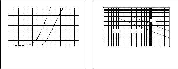
Fig.13. Typical reverse diode current.
IF = f(VSDS); conditions: VGS = 0 V; parameter Tj
Maximum Avalanche Current, IAS (A)
100 |
|
|
|
|
10 |
|
|
25 C |
|
1 |
Tj prior to avalanche = 150 C |
|
|
|
|
|
|
|
|
0.1 |
|
|
|
|
0.001 |
0.01 |
0.1 |
1 |
10 |
|
|
Avalanche time, tAV (ms) |
|
|
Fig.14. Maximum permissible non-repetitive avalanche current (IAS) versus avalanche time (tAV); unclamped inductive load
August 1999 |
6 |
Rev 1.100 |