

Basic Analog and Digital (Students guide, v13)
.pdfChapter 4: Basic Digital to Analog Conversion· Page 81
increases. Third, the largest error is 0.1 volts. This kind of data can be exceedingly useful in electronics design, and the automated testing process is a huge time saver.
The Voltage Follower
Let's use the voltage sweep to analyze what happens when the output of the D/A converter is connected to another circuit. We'll use the output of the D/A converter to drive an LED circuit. First we'll connect the D/A converter output directly to the input of the LED circuit. Then we'll use the voltage follower as an intermediate step between the D/A converter output and the LED circuit input.
P0
P1
P2
|
|
Vdd |
|
P7 |
|
|
|
|
|
|
|
|
|
LED |
|
|
|
|
|
2 kΩ |
|
|
|
|
|
|
|
1 kΩ |
|
2 kΩ |
|
|
8 |
5 |
|
|
|
||
|
|
P6 |
|
|
|
||
1 |
Vdd |
Vref |
|
|
|
|
|
|
2 kΩ |
1 kΩ |
|
270 Ω |
|||
|
/CS |
Vin(+) |
2 |
|
|
||
|
|
P5 |
|
|
|
||
7 |
CLK |
GND |
4 |
|
|
|
|
2 kΩ |
1 kΩ |
|
|
||||
6 |
|
|
|
|
|
||
D0 |
|
3 |
|
|
|
||
Vin(-) |
P4 |
|
|
|
|||
|
|
|
|
|
|||
|
ADC0831 |
|
2 kΩ |
2 kΩ |
|
|
|
|
|
|
|
|
|||
|
|
|
Vss |
|
Vss |
Vss |
Vss |
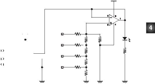
Figure 4-7 D/A Circuit without a Buffer.

Page 82 · Basic Analog and Digital
Table 4-1:D/A Converter Output Without Buffer
Decimal |
Binary |
|
DVM (volts) |
00 |
|
0000 |
___________ |
01 |
|
0001 |
___________ |
02 |
|
0010 |
___________ |
03 |
|
0011 |
___________ |
04 |
|
0100 |
___________ |
05 |
|
0101 |
___________ |
06 |
|
0110 |
___________ |
07 |
|
0111 |
___________ |
08 |
|
1000 |
___________ |
09 |
|
1001 |
___________ |
10 |
|
1010 |
___________ |
11 |
|
1011 |
___________ |
12 |
|
1100 |
___________ |
13 |
|
1101 |
___________ |
14 |
|
1110 |
___________ |
15 |
|
1111 |
___________ |
Figure 4-7 shows the D/A converter with an LED circuit added. The LED circuit is the "load" that the D/A converter must "drive". Run a voltage sweep on this circuit, and fill in the table below. Then try the voltage sweep using the output of the voltage follower in as shown in Figure 4-8. Fill out the same table of voltage sweep information for this second circuit, and compare the two. The voltage follower in Figure 4-7 is referred to as a buffer. The LED circuit has no voltage follower to separate it from the resistive ladder network. The LED is an "unbuffered" load for the D/A converter.
Chapter 4: Basic Digital to Analog Conversion· Page 83
|
|
|
|
|
|
|
|
|
Vdd |
|
|||
|
|
|
|
|
|
|
|
|
|
|
|
|
|
|
|
|
|
|
|
|
|
8 |
|
5 |
|
|
|
P0 |
|
|
|
|
1 |
Vdd/CS |
Vref |
|
|||||
|
|
|
Vin(+) |
2 |
|||||||||
|
|
||||||||||||
|
|
|
|
|
|
|
|
|
|
||||
P1 |
|
|
|
|
7 |
CLK |
|
GND |
4 |
||||
|
|
|
|||||||||||
6 |
|
||||||||||||
P2 |
|
|
|
D0 |
|
Vin(-) |
3 |
||||||
|
|
|
|||||||||||
|
|
|
|||||||||||
|
|
|
|
|
|
|
|
|
|
||||
|
|
|
|
|
|
|
|
|
|
||||
ADC0831
|
|
Vdd |
|
|
|
A |
|
|
|
LM358 |
|
P7 |
|
LED |
|
2 kΩ |
|
||
1 kΩ |
2 kΩ |
||
|
|||
P6 |
|
|
|
2 kΩ |
1 kΩ |
270 Ω |
|
|
|||
P5 |
|
|
|
2 kΩ |
1 kΩ |
|
|
|
|
||
P4 |
|
|
|
2 kΩ |
2 kΩ |
|
|
|
|
|
|
|
|
|
|
|
|
|
|
|
|
Vss |
Vss |
Vss |
Vss |
||||||||
Figure 4-8 D/A Circuit With a Buffer
Comparing the two tables, it should be fairly clear that the buffer (voltage follower) eliminated a problem caused by connecting the LED circuit directly to the D/A converter's output. The voltage of the D/A output without a buffer reached a maximum well below the D/A converter's 3 volt maximum. On the other hand, the buffered output went all the way to 3 volts with no problem.

Page 84 · Basic Analog and Digital
Table 4-2:D/A Converter Output with Buffer
Decimal |
Binary |
|
DVM (Volts) |
00 |
|
0000 |
___________ |
01 |
|
0001 |
___________ |
02 |
|
0010 |
___________ |
03 |
|
0011 |
___________ |
04 |
|
0100 |
___________ |
05 |
|
0101 |
___________ |
06 |
|
0110 |
___________ |
07 |
|
0111 |
___________ |
08 |
|
1000 |
___________ |
09 |
|
1001 |
___________ |
10 |
|
1010 |
___________ |
11 |
|
1011 |
___________ |
12 |
|
1100 |
___________ |
13 |
|
1101 |
___________ |
14 |
|
1110 |
___________ |
15 |
|
1111 |
___________ |
The reason for this goes back to Ohm's Law: V = I x R (voltage equals current multiplied by resistance). Each BASIC Stamp I/O pin can supply up to 20 mA of current. In the case of the resistive ladder network without the buffer, the BASIC Stamp I/O pins reached their maximum current output. Meanwhile, the resistance seen by the I/O pins stayed about the same. In other words, I x R reached a limit because I (the current) could no longer increase, and R is a fixed value. So the output voltage is equal to a current value that can't get any higher multiplied by a fixed resistance. This is why the voltage stops increasing.
Aside from isolating two circuits from each other, an op-amp in voltage follower configuration can typically supply more current than the circuit connected to its input. The name buffer is commonly used when a voltage follower is used to supply extra current.
The circuit from Figure 4-8 will also be used at the beginning of Chapter #5, so do not disassemble the circuit after completing Chapter #4.

Chapter 4: Basic Digital to Analog Conversion· Page 85
What have I learned?
On the lines below, insert the appropriate words from the list on the left.
|
A set of ___________ voltage values sent to the inputs of a resistive ladder |
|
binary |
network results in a ___________ voltage level at the output. This method |
|
is an inexpensive alternative to integrated circuits. Its advantages are |
||
discrete |
flexibility in resolution and low cost. Its main disadvantage is accuracy. |
|
The .BITX extension can be attached to a variable to select a particular |
||
bit |
||
___________ within a nibble, byte or word. This can be used to select bits |
||
output |
from a binary number in memory and set ___________ values equal to |
|
those bits. |
||
bit |
PBASIC can be used to address BASIC Stamp I/O pins a bit at a |
|
current |
___________ at a time, or alternatives exist for ___________ nibble, byte |
|
or word size groups of I/O pins. This allows the ___________ and output |
||
addressing |
values of the I/O pins to be addressed as groups of bits instead of as a |
|
single bit. |
||
direction |
A voltage ___________ can be run on a D/A converter. This allows one to |
|
sweep |
view the D/A converter's outputs for all possible binary inputs. The BASIC |
|
Stamp can be programmed to ___________ this process and display the |
||
automate |
data in a table format. |
|
The voltage follower can be used as a buffer, which can supply extra |
||
|
||
|
___________ to the input of a circuit connected to the D/A converter's |
|
|
output. |
Page 86 · Basic Analog and Digital
Questions
1.“1101” is what value in the decimal number system? What voltage would you expect from the D/A converter output if you sent it this binary number?
2.What function is provided by a D/A converter?
3.What are some of the advantages and disadvantages of the resistive ladder network?
4.Why does the D/A voltage “jump” from one value to another, unlike the voltage available on a pot?
5.How does the voltage follower solve the output voltage range problem when the D/A converter’s output is connected to the LED circuit’s input?
Challenge!
1.Create an 8 bit “resistive ladder” D/A converter. Draw the complete schematic.
2.Write a program that will step through 256 different analog voltages. Each voltage should be present for 100 milliseconds on the voltmeter.

Chapter 4: Basic Digital to Analog Conversion· Page 87
Why did I learn it?
There are many different “real world” circuits that require some sort of analog voltage. For example, when you listen to a compact disc, you’re listening to sounds that started as analog signals from a microphone. Then the signal underwent the A/D process when it was digitized. The CD player then performs the D/A conversion using the digital information on the CD. The analog signal is amplified and played on a speaker.
When designing commercial products, it is your responsibility to determine the most appropriate (and cost effective) method to accomplish a given task. A resistive D/A converter is a very economical method to get an analog voltage from a digital device.
How can I apply this?
You've just built a variable voltage source and a digital voltmeter on the same breadboard. You also used some PBASIC Programming techniques to obtain information about the converter using a voltage sweep. One application of this can be testing circuits, but there are many others. In Chapter #5, we'll see how PBASIC can be used to control the volume of tones emitted by a speaker. In Chapter #7, we'll use D/A conversion to control the brightness of an LED transmitting a signal to a photoresistor.
The applications for D/A and A/D interfaces combined with a microcontroller are only limited by one's imagination. These techniques can be applied to automated houses, irrigation systems, rocket guidance systems, and robotics to name a few. Control systems engineering is a field of study within electrical engineering that you might look into if you find designing such systems interesting.

Chapter 5: Time Varying Signals · Page 89
Chapter #5: Time Varying Signals
In this chapter we'll view signals with the Stamp-O-Scope. To do this we'll use the BASIC Stamp along with the A/D and D/A circuits built in Chapters #3 and #4 to emulate the function of an oscilloscope.
The voltage output of the resistive ladder network will be varied with time, and the changes will be tracked using our oscilloscope emulator, the Stamp-O-Scope. The Stamp-O-Scope will gather its input voltage data from the ADC0831 and display it graphically in the Debug Terminal.
We'll view two different signals using the Stamp-O-Scope, and we'll use the D/A converter to adjust the attributes of both signals. The first signal we'll work with is called a triangle wave, and the second is called a pulse train. The LED will be used to monitor the activity of both signals.
Unlike a normal oscilloscope, the Stamp-O-Scope cannot monitor voltage signals at frequencies in the audible sound range. However, the BASIC Stamp can easily send a voltage signal in the audible sound range via the D/A converter. This signal can be used to make a speaker emit tones of adjustable pitch and volume.
The pitch and volume will be adjusted by changing two of the pulse train's properties. But first, let's get started and view these properties with the Stamp-O-Scope.
Also in this experiment, the BASIC Stamp is used to generate sine waves (see Figure 5-1) of adjustable frequency. These sine waves are used to make musical notes.

Page 90 · Basic Analog and Digital
Oscilloscope A device that measures and displays time-varying voltage signals. The oscilloscope is a common tool used by many electronics technicians and engineers to display these signals. The signals of interest often repeat themselves many times each second. The oscilloscope can be used to view the general shape of the signal, how fast it repeats itself, and the maximum and minimum voltage values of the signal as it repeats itself
Figure 5-1
Oscilloscope displaying a sine wave output from Program Listing 5.3.
Frequency The rate at which a periodic time varying signal repeats itself. Frequency is measured in repetitions per second. The name Hertz (Hz) is used when referring to frequency. One Hertz is one repetition per second, that is:
1 Hz = 1 repetition/second = 1/s
Parts Required
The same circuit used in Chapter #4, Figure 4-8 is used to begin this experiment. Later, the LED circuit is replaced with a piezoelectric speaker circuit. For this experiment you'll need the following parts:
(6) 2 k resistors
(3) 1 k resistors
(1) ADC0831 A/D Converter
(10) Jumper wires
(1) Piezoelectric speaker