

An introduction to the PIC microcontroller
.pdfEE2801 -- Lecture 19
An Introduction To The
PIC Microcontroller
EE2801-L19P01

The PIC 16F87X Series Microcontroller
The PIC Series of microcontrollers is representative of the current industry trend towards highly capable, low-cost, processors for embedded applications. Although they are not suited to everything, they can do a lot!
However, they are quite a bit different that what we’re used to at this point!
Some of the characteristics of the PIC 16F87X series are:
Only 35 instructions!
All instructions (except branch) execute in 1 cycle. Eight level deep hardware stack.
4K word program space, 192 bytes of RAM
Internal A/D converter, serial port, digital IO ports, timers, and more!
Remember, what you are about to see will look completely different than anything you’ve seen so far!
However, all of the techniques we’ve used and the concepts we’ve learned are directly applicable!
EE2801-L19P02

The PIC 16F87X Family Capabilities
The following table summarizes the capabilities of the PIC16F87X series components. Although when we use the compiler we’ll set the processor type to 16F877, that’s only because each component in the family is compatible. The actual version we’ll use is the PIC16F874:
PIC16F87X
|
|
|
|
|
|
|
|
|
|
|
|
|
|
|
|
|
|
|
|
|
Key Features |
|
|
|
|
|
|
PICmi croô Mid-Range Referenc e |
PIC16F873 |
PIC16F874 |
PIC16F876 |
|
PIC16F877 |
|
Manual (DS33023) |
|
|
|
|
|
|
|
|
|
|
|
|
|
|
|
|
|
|
|
|
Operating Frequency |
DC - 20 MHz |
DC - 20 MHz |
DC - 20 MHz |
|
DC - 20 MHz |
|
|
|
|
|
|
|
|
Resets (and Delays) |
POR, BOR |
POR, BOR |
POR, BOR |
|
POR, BOR |
|
|
(PWRT, OST) |
(PWRT, OST) |
(PWRT, OST) |
|
(PWRT, OST) |
|
|
|
|
|
|
|
|
FLASH Program Memory |
4K |
4K |
8K |
|
8K |
|
(14-bit words) |
|
|
|
|
|
|
|
|
|
|
|
|
|
Data Memory (bytes) |
192 |
192 |
368 |
|
368 |
|
|
|
|
|
|
|
|
EEPROM Data Memory |
128 |
128 |
256 |
|
256 |
|
|
|
|
|
|
|
|
Interrupts |
13 |
14 |
13 |
|
14 |
|
|
|
|
|
|
|
|
I/O Ports |
Ports A,B,C |
Ports A,B,C,D,E |
Ports A,B,C |
|
Ports A,B,C,D,E |
|
|
|
|
|
|
|
|
Timers |
3 |
3 |
3 |
|
3 |
|
|
|
|
|
|
|
|
Capture/Compare/PWM modules |
2 |
2 |
2 |
|
2 |
|
|
|
|
|
|
|
|
Serial Communications |
MSSP, USART |
MSSP, USART |
MSSP, USART |
|
MSSP, USART |
|
|
|
|
|
|
|
|
Parallel Communications |
- |
PSP |
- |
|
PSP |
|
|
|
|
|
|
|
|
10-bit Analog-to-Digital Module |
5 input channels |
8 input channels |
5 input channels |
8 |
input channels |
|
|
|
|
|
|
|
|
Instruction Set |
35 Instructions |
35 Instructions |
35 Instructions |
|
35 Instructions |
|
|
|
|
|
|
|
|
EE2801-L19P03

The PIC16F874 Architecture
13 |
|
Data Bus |
8 |
|
Program Counter |
|
|
FLASH |
|
|
|
|
|
|
|
Program |
|
|
|
Memory |
|
RAM |
|
|
8 Level Stack |
|
|
|
File |
|
|
|
(13-bit) |
|
|
|
Registers |
|
|
|
|
|
Program |
14 |
|
|
|
|
|
|
|
|
|
|
|
|
|
|
|
|
|
|
|
|
|
|
|
|
|
|
|
RAM Addr (1) |
|
|
9 |
|
|
|
|
|||||||||
Bus |
|
|
|
|
|
|
|
|
|
|
|
|
||||||||||
|
|
|
|
|
|
|
|
|
|
|
|
|
||||||||||
|
|
|
|
|
|
|
|
|
|
|
|
|
Addr MUX |
|
|
|
||||||
|
|
Instruction reg |
|
|
|
|
|
|||||||||||||||
|
|
|
|
|
|
|
|
|
|
|
|
|
|
|
|
|
||||||
|
|
|
|
|
|
|
|
Direct Addr 7 |
|
|
|
|
|
|
|
8 |
|
Indirect |
||||
|
|
|
|
|
|
|
|
|
|
|
|
|
|
|
|
|||||||
|
|
|
|
|
|
|
|
|
|
|
|
|
|
|
|
|
|
Addr |
||||
|
|
|
|
|
|
|
|
|
|
|
|
|
|
|
|
|
|
|||||
|
|
|
|
|
|
|
|
|
|
|
|
|
|
|
|
|
|
|
|
|
||
|
|
|
|
|
|
|
|
|
|
|
|
|
|
|
|
|
|
|
|
|
|
|
|
|
|
|
|
|
|
|
|
|
|
|
|
|
|
|
|
|
FSR reg |
|
|||
|
|
|
|
|
|
|
|
|
|
|
|
|
|
|
|
|
|
|
|
|
|
|
|
|
|
|
|
|
|
|
|
|
|
|
|
|
|
|
|
|
|
|
|
|
|
|
|
|
|
8 |
|
|
|
|
|
|
|
|
STATUS reg |
|
||||||||
|
|
|
|
|
|
|
|
|
|
|
|
|
||||||||||
|
|
|
|
|
|
|
|
|
|
|
|
|
||||||||||
|
|
|
|
|
|
|
|
|
|
|
|
|
|
|
|
|
||||||
|
|
|
|
|
|
|
|
|
|
|
|
|
|
|
|
|||||||
|
|
|
|
|
|
|
|
|
|
|
|
|
|
|
|
|
|
|
|
|
|
|
|
|
Power-up |
3 |
MUX |
|
|
|
||
|
|
|
|
|
|
|
Timer |
|
|
|
Instruction |
Oscillator |
|
|
|
Decode & |
Start-up Timer |
|
ALU |
|
Control |
|
|
|
|
Power-on |
|
|
|
|
|
8 |
|
|
|
|
Reset |
|
|
|
Timing |
Watchdog |
|
W reg |
|
Generation |
Timer |
|
|
|
|
|
||
OSC1/CLKIN |
|
Brown-out |
|
|
OSC2/CLKOUT |
|
Reset |
|
|
|
|
|
|
|
|
|
In-Circuit |
|
|
|
|
Debugger |
|
|
|
|
Low-Voltage |
|
|
|
|
Programming |
|
Parallel Slave Port |
|
|
MCLR VDD, VSS |
|
|
Timer0 |
Timer1 |
Timer2 |
|
10-bit A/D |
Data EEPROM |
|
CCP1,2 |
|
Synchronous |
|
USART |
|
|
|
Serial Port |
|
||
|
|
|
|
|
|
|
|
|
|
|
|
|
|
PORTA |
|
|
RA0/AN0 |
|
RA1/AN1 |
|
RA2/AN2/VREF- |
|
RA3/AN3/VREF+ |
|
RA4/T0CKI |
|
RA5/AN4/SS |
PORTB |
RB0/INT |
|
|
|
RB1 |
|
RB2 |
|
RB3/PGM |
|
RB4 |
|
RB5 |
|
RB6/PGC |
PORTC |
RB7/PGD |
|
|
|
RC0/T1OSO/T1CKI |
|
RC1/T1OSI/CCP2 |
|
RC2/CCP1 |
|
RC3/SCK/SCL |
|
RC4/SDI/SDA |
|
RC5/SDO |
|
RC6/TX/CK |
|
RC7/RX/DT |
PORTD |
|


 RD7/PSP7:RD0/PSP0
PORTE |
RE0/AN5/RD |
RE1/AN6/WR |
RE2/AN7/CS |
Devi ce |
Program |
Data Memo ry |
Data |
|
FLASH |
|
EEPROM |
|
|
|
|
PIC16F874 |
4K |
192 Bytes |
128 Bytes |
|
|
|
|
PIC16F877 |
8K |
368 Bytes |
256 Bytes |
|
|
|
|
EE2801-L19P04

The PIC16F874 Program And Stack Memory Map
Instead of having a large memory space outside the processor and a small memory space inside the processor (the registers) like we do in the 80x86, the PIC does two things. First, it divides memory into two main spaces: program memory and data memory. For program memory, the map looks as follows:
PC<12:0>
CALL, RETURN |
13 |
RETFIE, RETLW
Stack Level 1
Stack Level 2
|
|
Stack Level 8 |
|
|
|
|
|
|
|
|
|
|
|
|
|
|
|
|
|
Reset Vector |
0000h |
|
|
|
|
|
|
|
|
|
|
|
|
|
|
|
|
|
|
|
|
|
|
|
|
|
|
|
|
Interrupt Vector |
0004h |
|
|
|
|
|
0005h |
|
|
|
|
|
|
||
|
|
|
|
||
On-Chip |
|
Page 0 |
|
|
|
|
|
|
|
|
|
07FFh
Program
Memory |
0800h |
|
|
|
Page 1 |
|
0FFFh |
|
1000h |
Note: The unused space in this memory map is used in other family processors.
1FFFh
EE2801-L19P05
The PIC16F874 Register File Map
Indirect addr.(*) |
00h |
|
TMR0 |
01h |
|
|
02h |
|
PCL |
||
|
03h |
|
STATUS |
||
|
04h |
|
FSR |
||
|
05h |
|
PORTA |
||
|
06h |
|
PORTB |
||
|
07h |
|
PORTC |
||
|
08h |
|
PORTD (1) |
||
PORTE (1) |
09h |
|
PCLATH |
0Ah |
|
|
0Bh |
|
INTCON |
||
|
0Ch |
|
PIR1 |
||
|
0Dh |
|
PIR2 |
||
|
0Eh |
|
TMR1L |
||
|
0Fh |
|
TMR1H |
||
|
10h |
|
T1CON |
||
|
11h |
|
TMR2 |
||
|
12h |
|
T2CON |
||
|
13h |
|
SSPBUF |
||
|
14h |
|
SSPCON |
||
|
15h |
|
CCPR1L |
||
|
16h |
|
CCPR1H |
||
|
17h |
|
CCP1CON |
||
|
18h |
|
RCSTA |
||
|
19h |
|
TXREG |
||
|
1Ah |
|
RCREG |
||
|
1Bh |
|
CCPR2L |
||
|
1Ch |
|
CCPR2H |
||
|
1Dh |
|
CCP2CON |
||
|
1Eh |
|
ADRESH |
||
|
1Fh |
|
ADCON0 |
||
|
20h |
|
General |
||
|
||
Purpose |
|
|
Register |
|
|
96 Bytes |
|
|
|
7Fh |
|
Bank 0 |
|
Indirect addr.(*) |
80h |
OPTION_REG |
81h |
|
|
PCL |
82h |
|
|
STATUS |
83h |
|
|
FSR |
84h |
|
|
TRISA |
85h |
|
|
TRISB |
86h |
|
|
TRISC |
87h |
|
|
TRISD (1) |
88h |
TRISE (1) |
89h |
PCLATH |
8Ah |
|
|
INTCON |
8Bh |
|
|
PIE1 |
8Ch |
|
|
PIE2 |
8Dh |
|
|
PCON |
8Eh |
|
8Fh |
|
|
|
90h |
SSPCON2 |
91h |
|
|
PR2 |
92h |
|
|
SSPADD |
93h |
|
|
SSPSTAT |
94h |
|
95h |
|
|
|
96h |
|
97h |
TXSTA |
98h |
|
99h |
SPBRG |
|
|
9Ah |
|
|
|
9Bh |
|
9Ch |
|
9Dh |
ADRESL |
9Eh |
|
9Fh |
ADCON1 |
|
|
A0h |
|
|
General |
|
Purpose |
|
Register |
|
96 Bytes |
|
|
FFh |
Bank 1 |
|
Indirect addr.(*) |
100h |
|
101h |
TMR0 |
|
|
102h |
PCL |
|
|
103h |
STATUS |
|
|
104h |
FSR |
|
|
105h |
|
|
|
106h |
PORTB |
|
|
107h |
|
|
|
108h |
|
|
|
109h |
|
|
|
10Ah |
PCLATH |
|
|
10Bh |
INTCON |
|
|
10Ch |
EEDATA |
|
|
|
EEADR |
10Dh |
|
10Eh |
EEDATH |
|
|
10Fh |
EEADRH |
|
|
110h |
|
120h
accesses 20h-7Fh
16Fh
170h
17Fh
Bank 2
|
File |
Address |
|
|
|
Indirect addr.(*) |
180h |
OPTION_REG |
181h |
|
|
PCL |
182h |
|
|
STATUS |
183h |
|
|
FSR |
184h |
|
185h |
|
|
TRISB |
186h |
|
187h |
|
|
|
188h |
|
189h |
PCLATH |
18Ah |
|
|
INTCON |
18Bh |
|
|
EECON1 |
18Ch |
|
|
EECON2 |
18Dh |
|
|
Reserved(2) |
18Eh |
Reserved(2) |
18Fh |
|
190h |
1A0h
accesses A0h - FFh
1EFh
1F0h
1FFh
Bank 3
EE2801-L19P06

“Registers” In The PIC Microcontrollers
|
|
|
|
|
|
|
|
|
|
|
|
|
|
|
|
|
|
Value on: |
Value on |
||
Addr es |
|
|
|
|
|
|
|
|
|
|
|
|
|
|
|
|
|
all other |
|||
Name |
Bi t 7 |
Bit 6 |
Bit 5 |
|
Bit 4 |
Bit 3 |
Bit 2 |
|
Bit 1 |
Bit 0 |
POR, |
||||||||||
s |
|
|
resets |
||||||||||||||||||
|
|
|
|
|
|
|
|
|
|
|
|
|
|
|
|
|
BOR |
||||
|
|
|
|
|
|
|
|
|
|
|
|
|
|
|
|
|
|
(2) |
|||
|
|
|
|
|
|
|
|
|
|
|
|
|
|
|
|
|
|
|
|
||
|
|
|
|
|
|
|
|
|
|
|
|
|
|
|
|
|
|
|
|
|
|
|
|
|
|
|
|
|
|
|
|
|
|
|
|
|
|
|
|
|
|
|
|
Bank 0 |
|
|
|
|
|
|
|
|
|
|
|
|
|
|
|
|
|
|
|
|
|
|
|
|
|
|
|
|
|
|
|
|
|
|
|
||||||||
00h(4) |
INDF |
Addressing this location uses contents of FSR to address data memory (not a physical register) |
0000 |
0000 |
0000 |
0000 |
|||||||||||||||
01h |
TMR0 |
Timer0 moduleís register |
|
|
|
|
|
|
|
|
|
|
|
|
|
|
xxxx xxxx |
uuuu uuuu |
|||
02h(4) |
PCL |
Program Counter's (PC) Least Significant Byte |
|
|
|
|
|
|
|
|
|
0000 |
0000 |
0000 |
0000 |
||||||
03h(4) |
STATUS |
IRP |
RP1 |
RP0 |
|
TO |
|
PD |
|
Z |
D |
C |
C |
0001 |
1xxx |
000q |
quuu |
||||
04h(4) |
FSR |
Indirect data memory address pointer |
|
|
|
|
|
|
|
|
|
|
|
|
xxxx xxxx |
uuuu uuuu |
|||||
05h |
PORTA |
ó |
ó |
PORTA Data Latch when written: PORTA pins when read |
|
--0x 0000 |
--0u 0000 |
||||||||||||||
06h |
PORTB |
PORTB Data Latch when written: PORTB pins when read |
|
|
|
|
|
|
xxxx xxxx |
uuuu uuuu |
|||||||||||
07h |
PORTC |
PORTC Data Latch when written: PORTC pins when read |
|
|
|
|
|
|
xxxx xxxx |
uuuu uuuu |
|||||||||||
08h(5) |
PORTD |
PORTD Data Latch when written: PORTD pins when read |
|
|
|
|
|
|
xxxx xxxx |
uuuu uuuu |
|||||||||||
09h(5) |
PORTE |
ó |
ó |
ó |
|
ó |
|
|
ó R |
|
E2 |
|
RE1 |
RE0 |
---- -xxx |
---- -uuu |
|||||
0Ah(1,4) |
PCLATH |
ó |
ó |
ó |
|
Write Buffer for the upper 5 bits of the Program Counter |
---0 0000 |
---0 0000 |
|||||||||||||
0Bh(4) |
INTCON |
GIE |
PEIE |
T0IE |
|
INTE |
RBIE |
|
T0IF |
|
INTF |
RBIF |
0000 |
000x |
0000 |
000u |
|||||
0Ch |
PIR1 |
PSPIF(3) |
ADIF |
RCIF |
|
TXIF |
SSPIF |
CCP1IF |
|
TMR2IF |
TMR1IF |
0000 |
0000 |
0000 |
0000 |
||||||
0Dh |
PIR2 |
ó |
(6) |
ó |
|
EEIF |
BCLIF |
ó |
|
|
ó |
CCP2IF |
-r-0 0--0 |
-r-0 0--0 |
|||||||
0Eh |
TMR1L |
Holding register for the Least Significant Byte of the 16-bit TMR1 register |
|
|
|
xxxx xxxx |
uuuu uuuu |
||||||||||||||
0Fh |
TMR1H |
Holding register for the Most Significant Byte of the 16-bit TMR1 register |
|
|
|
xxxx xxxx |
uuuu uuuu |
||||||||||||||
10h |
T1CON |
ó |
ó |
T1CKPS1 |
|
T1CKPS0 |
T1OSCEN |
T1SYNC |
TMR1CS |
TMR1ON |
--00 0000 |
--uu uuuu |
|||||||||
11h |
TMR2 |
Timer2 moduleís register |
|
|
|
|
|
|
|
|
|
|
|
|
|
|
0000 |
0000 |
0000 |
0000 |
|
12h |
T2CON |
ó |
TOUTPS3 |
TOUTPS2 |
|
TOUTPS1 |
TOUTPS0 |
TMR2ON |
T2CKPS1 |
T2CKPS0 |
-000 0000 |
-000 0000 |
|||||||||
13h |
SSPBUF |
Synchronous Serial Port Receive Buffer/Transmit Register |
|
|
|
|
|
|
xxxx xxxx |
uuuu uuuu |
|||||||||||
14h |
SSPCON |
WCOL |
SSPOV |
SSPEN |
|
CKP |
SSPM3 |
SSPM2 |
|
SSPM1 |
SSPM0 |
0000 |
0000 |
0000 |
0000 |
||||||
15h |
CCPR1L |
Cap ture/Compare/PWM Register1 (LSB) |
|
|
|
|
|
|
|
|
|
xxxx xxxx |
uuuu uuuu |
||||||||
16h |
CCPR1H |
Cap ture/Compare/PWM Register1 (MSB) |
|
|
|
|
|
|
|
|
|
xxxx xxxx |
uuuu uuuu |
||||||||
17h |
CCP1CON |
ó |
ó |
CCP1X |
|
CCP1Y |
CCP1M3 |
CCP1M2 |
|
CCP1M1 |
CCP1M0 |
--00 0000 |
--00 0000 |
||||||||
18h |
RCSTA |
SPEN |
RX9 |
SREN |
|
CREN |
ADDEN |
FERR |
|
OERR |
RX9D |
0000 |
000x |
0000 |
000x |
||||||
19h |
TXREG |
USART Transmit Data Register |
|
|
|
|
|
|
|
|
|
|
|
|
0000 |
0000 |
0000 |
0000 |
|||
1Ah |
RCREG |
USART Receive Data Register |
|
|
|
|
|
|
|
|
|
|
|
|
0000 |
0000 |
0000 |
0000 |
|||
1Bh |
CCPR2L |
Cap ture/Compare/PWM Register2 (LSB) |
|
|
|
|
|
|
|
|
|
xxxx xxxx |
uuuu uuuu |
||||||||
1Ch |
CCPR2H |
Cap ture/Compare/PWM Register2 (MSB) |
|
|
|
|
|
|
|
|
|
xxxx xxxx |
uuuu uuuu |
||||||||
1Dh |
CCP2CON |
ó |
ó |
CCP2X |
|
CCP2Y |
CCP2M3 |
CCP2M2 |
|
CCP2M1 |
CCP2M0 |
--00 0000 |
--00 0000 |
||||||||
1Eh |
ADRESH |
A/D Result Register High Byte |
|
|
|
|
|
|
|
|
|
|
|
|
xxxx xxxx |
uuuu uuuu |
|||||
1Fh |
ADCON0 |
ADCS1 |
ADCS0 |
CHS2 |
|
CHS1 |
CHS0 |
|
GO/ |
|
|
ó A |
DON |
0000 |
00-0 |
0000 |
00-0 |
||||
|
|
DONE |
|
||||||||||||||||||
|
|
|
|
|
|
|
|
|
|
|
|
|
|
|
|
|
|
|
|
||
EE2801-L19P07

How To Deal With All These Registers!!!
R/W-0 |
R/W-0 R/W-0 |
R-1 |
R-1 |
|
R/W-x |
R/W-x |
R/W-x |
|
|
||||
|
|
|
|
|
|
|
|
|
|
|
|
|
|
IRP |
RP1 |
RP0 |
|
TO |
|
PD |
|
Z |
DC |
C |
|
R = Readable bit |
|
|
|
|
|
|
|
|
|
|
|
|
|
|
W = Writable bit |
bit7 |
|
|
|
|
|
|
|
|
|
|
bit0 |
|
|
|
|
|
|
|
|
|
|
|
|
|
U = Unimplemented bit, |
||
|
|
|
|
|
|
|
|
|
|
|
|
|
|
|
|
|
|
|
|
|
|
|
|
|
|
|
read as ë0í |
|
|
|
|
|
|
|
|
|
|
|
|
|
- n= Value at POR reset |
bit 7: |
IRP: |
|
|
|
|
|
|
|
|
|
|
|
|
|
|
|
|
|
|
|
|
|
|
|
|
||
Register Bank Select bit (used for indirect addressing) |
|
|
|
||||||||||
1 = Bank 2, 3 (100h - 1FFh)
0 = Bank 0, 1 (00h - FFh)
bit |
6-5: |
RP1:RP0: Register Bank Select bits (used for direct addressing) |
||||||
|
|
11 = Bank 3 (180h - 1FFh) |
||||||
|
|
10 = Bank 2 (100h - 17Fh) |
||||||
|
|
01 = Bank 1 (80h - FFh) |
||||||
|
|
00 = Bank 0 (00h - 7Fh) |
||||||
|
|
Each bank is 128 bytes |
||||||
|
|
|
|
|
|
|
|
|
bit |
4: |
TO: Time-out bit |
||||||
|
|
1 |
= After power-up, CLRWDT instruction, or SLEEP instruction |
|||||
|
|
0 |
= A WDT time-out occurred |
|||||
|
|
|
|
|
|
|
|
|
bit |
3: |
PD: Power-down bit |
||||||
|
|
1 |
= After power-up or by the CLRWDT instruction |
|||||
|
|
0 |
= By execution of the SLEEP instruction |
|||||
bit |
2: |
Z: Zero bit |
||||||
|
|
1 |
= The result of an arithmetic or logic operation is zero |
|||||
|
|
0 |
= The result of an arithmetic or logic operation is not zero |
|||||
|
|
|
|
|
|
|
||
bit |
1: |
DC: Digit carry/borrow bit (ADDWF, ADDLW,SUBLW,SUBWF instructions) |
||||||
|
|
(for borrow the polarity is reversed) |
||||||
|
|
1 |
= A carry-out from the 4th low order bit of the result occurred |
|||||
|
|
0 |
= No carry-out from the 4th low order bit of the result |
|||||
|
|
|
|
|
||||
bit |
0: |
C: Carry/borrow bit (ADDWF, ADDLW,SUBLW,SUBWF instructions) |
||||||
|
|
1 |
= A carry-out from the most significant bit of the result occurred |
|||||
|
|
0 |
= No carry-out from the most significant bit of the result occurred |
|||||
Note: For borrow the polarity is reversed. A subtraction is executed by adding the twoís complement of the second operand. For rotate ( RRF, RLF) instructions, this bit is loaded with either the high or low order bit of the source register.
EE2801-L19P08
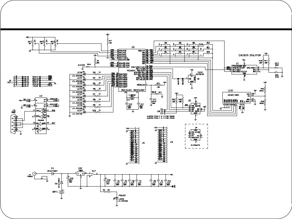
An Example PIC-Based System
EE2801-L19P09