

Appendix B.Analytical spiral inductor model
.pdfRadio Frequency Circuit Design. W. Alan Davis, Krishna Agarwal
Copyright 2001 John Wiley & Sons, Inc.
Print ISBN 0-471-35052-4 Electronic ISBN 0-471-20068-9
APPENDIX B
Analytical Spiral Inductor
Model
Modeling equations for spiral inductors given in [1,2] are collected here for convenience. A straight line of length l, width w, thickness t, resistivity , and in a material of permeability 0 has the following inductance:
|
|
|
|
|
|
|
|
|
|
|
L D 2 ln |
|
1 |
|
|
|
|
|
|
|
|
|
B.1 |
|||||||||||||||
|
|
|
|
|
|
|
|
|
|
|
|
|
|
|
0l |
|
|
2l |
|
|
|
|
|
|
|
|
|
|
|
|
|
|
||||||
where |
|
|
|
|
|
|
|
|
|
|
|
|
|
|
|
|
|
|
|
|
|
|
|
|
|
|
|
|
|
|
|
|
|
|
|
|
|
|
|
|
|
|
|
|
|
|
|
|
|
|
|
|
|
|
|
|
|
|
|
|
|
|
|
|
|
|
|
|
|
|
|
|
|
||||
|
|
|
25 |
|
|
|
1 |
|
w |
|
|
|
|
|
|
t |
|
2 |
|
|
|
w |
|
|
|
|
|
|
|
|||||||||
ln |
|
|
|
|
|
|
2 ln 1 |
|
|
|
|
|
|
|
2 ln 1 |
|
|
w |
|
2 |
||||||||||||||||||
2c |
D 12 6 |
|
|
C |
w |
|
|
C t |
|
C |
t |
|
||||||||||||||||||||||||||
|
t |
|
|
|
|
|
|
|
|
|
|
|
||||||||||||||||||||||||||
|
|
|
|
|
|
|
|
|
|
|
|
|
|
|
C w arctan t |
|
|
|
|
|
|
|
|
|||||||||||||||
|
|
C |
3 |
t |
arctan w |
|
|
|
|
|
|
|
|
B.2 |
||||||||||||||||||||||||
|
|
|
|
2 |
|
|
w |
|
|
|
|
|
|
|
t |
|
|
|
|
t |
|
|
|
|
|
|
w |
|
|
|
|
|
|
|
|
|
|
|
|
2c D |
|
|
|
|
|
|
|
|
|
|
|
|
|
|
|
|
|
|
|
|
|
|
|
|
|
|
|
|
|
||||||||
|
w2 C t2 |
|
|
|
|
|
|
|
|
|
|
|
|
|
|
|
|
|
|
|
|
|
|
|
|
|
|
|
B.3 |
|||||||||
If inhomogeneous current density across the conductor cross section is to be considered, an additional expression is found in [1].
The single-loop inductor is illustrated in Fig. B.1 where the total angular rotation, 0, is somewhat less than 360°. The inductance is found by numerical integration of the following equation:
L D |
2 w2 |
0 |
|
p |
|
0p2 2 cos p2 F d |
B.4 |
||||
|
0 |
0 |
/ |
2 |
|
|
|
|
|
|
|
where |
|
|
|
|
|
|
|
|
|
|
|
F D G ro, ro G ri, ro G ro, ri C G ri, ri |
B.5 |
||||||||||
286

ANALYTICAL SPIRAL INDUCTOR MODEL |
287 |
φo r o
r i
W
|
|
|
FIGURE B.1 Single-loop inductor. |
|
|
|
|
|
|
|
|
|||||||||||||||||
G r1 |
, r2 D |
3 R3 C |
3 r1r2R cos p2 |
|
|
|
|
|
|
|
|
|
|
|||||||||||||||
|
|
1 |
|
|
|
2 |
|
p2 |
|
|
|
|
|
|
|
|
|
|
|
|
||||||||
|
|
|
|
2 r13 cos |
arcsin |
|
|
|
|
B.6 |
||||||||||||||||||
|
|
|
|
|
|
|
|
|
|
|
|
|
|
|
|
r2 |
|
r1 cos |
|
|
p2 |
|
||||||
|
|
C |
|
|
|
|
|
|
|
|
|
|
|
r1j sin p2 j |
|
|
||||||||||||
|
|
|
3 |
|
|
|
|
|
|
|
|
|
||||||||||||||||
|
R D |
|
|
|
|
|
|
|
|
|
|
|
|
|
|
|||||||||||||
|
r12 C r22 2r1r2 cos p |
|
|
|
|
|
|
|
|
|
|
|
B.7 |
|||||||||||||||
|
2 |
. |
|
|
|
|
|
|
|
|
|
|||||||||||||||||
The inductance of a circular spiral with n turns (with air bridge) consists of n static inductances, Li, i D 1, . . . , n, as found above plus mutual inductance terms between the ith and jth line segments. This mutual inductance is
Mij D pab kij |
kij |
K kij kij E kij |
B.8 |
||||
|
2 |
|
|
2 |
|
|
|
where |
|
|
|
|
|
||
kij D |
4ab |
|
|
B.9 |
|||
|
|
|
|
||||
a C b 2 |
|
|
|||||
|
a D ri C i 0.5 w C s |
B.10 |
|||||
|
b D ri C j 0.5 w C s |
B.11 |
|||||
In this expression for the mutual inductance, ri is the inner radius of the inner most turn of the circular spiral, w is the conductor width, and s is the spacing between turns. The outer most radius of the outer most turn is determined by these parameters together with the number of turns, n. The K kij and E kij are the complete elliptic integrals of the first and second kind, respectively. If there is a ground plane underneath the spiral conductor a distance h away, there is an additional mirrored mutual inductance, Mmij given by Eq. (B.8) where
288 |
ANALYTICAL SPIRAL INDUCTOR MODEL |
|
|
|
kij D |
4ab |
B.12 |
|
|
||
|
4h2 C a C b 2 |
||
and where a and b are given by Eqs. (B.10) and (B.11). The inductance of the multiple-turn circular spiral is then
n |
n 1 n |
n |
n |
|
|
|
|
L D Li C 2 |
iD1 jDiC1 |
Mij C |
Mijm |
iD1 |
iD1 jD1 |
||
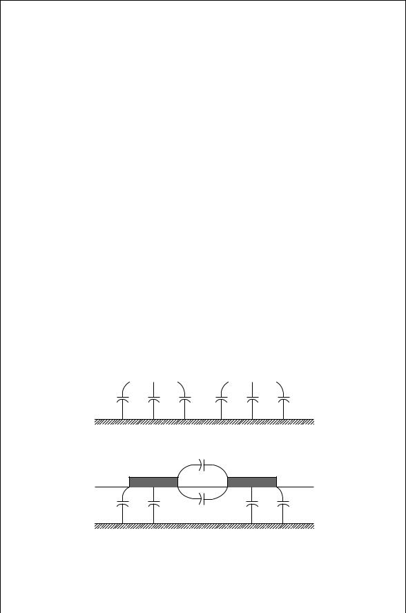
The associated capacitances are shown in Fig. B.2, which were
[3,4,5]: |
|
|
|
|
|
|
|
|
|
|
|
|
ε0 K k0 |
|
|
|
|
|
|
||||||||||
|
|
|
|
|
|
|
|
|
Cga D |
|
|
|
|
|
|
||||||||||||||
|
|
|
|
|
|
|
|
|
|
|
|
|
|
|
|
|
|
|
|
|
|
|
|
||||||
|
|
|
|
|
|
|
2 K k |
|
|
|
|
|
|
||||||||||||||||
The arguments of the elliptic integrals are |
2h |
|
|
|
|
|
|
||||||||||||||||||||||
|
|
|
|
|
|
|
|
k D h |
h C |
|
|
|
|
|
|
||||||||||||||
|
|
|
|
|
|
|
|
|
|
|
s |
|
|
s |
|
w |
|
|
|
|
|
|
|||||||
|
|
|
|
|
|
|
k0 D |
|
|
|
|
|
|
|
|
|
|
|
|
|
|
||||||||
|
|
|
|
|
|
1 k2 |
|
|
|
|
|
|
|
|
|
|
|
|
|||||||||||
The dielectric coupling capacitance is |
|
|
|
|
|
|
|
s/h |
|
|
|
|
|
|
|||||||||||||||
|
D |
|
|
|
4 h C |
|
|
|
|
|
|
|
C |
|
|
εr2 |
|||||||||||||
Cge |
|
ε0εr |
ln coth |
|
s |
0.65Cf |
|
0.02 |
p |
|
|
1 |
1 |
|
|||||||||||||||
|
|
|
|
|
|
|
|
|
|
|
εr |
|
|
|
|
||||||||||||||
|
|
|
|
|
|
|
|
|
|
|
|
|
|
|
|
|
|
|
|
|
|
|
|
|
|
|
|
|
|
|
|
|
|
|
|
|
|
|
|
|
|
|
|
|
|
|
|
|
|
|
|
|
|
|
|
|
|
|
|
B.13
given by
B.14
B.15
B.16
B.17
C f |
C m |
C f' |
C f' |
C m |
C f |
(a ) Even Mode
C ga
C f |
C m |
C m |
C f |
|
|
C ge |
|
(b ) Odd Mode
FIGURE B.2 Capacitances associated with the coupled microstrip.

REFERENCES 289
The main capacitance to ground is
|
|
|
|
|
Cm D |
ε0εrw |
|
B.18 |
||||
|
|
|
|
|
h |
|||||||
The fringing capacitances are |
|
|
|
|
|
|
|
|
|
|
||
|
1 |
|
p |
|
|
|
ε0εrw |
|
||||
|
|
εeff |
|
|||||||||
Cf D |
|
|
|
|
|
|
|
|
|
|
B.19 |
|
2 |
|
cZ0 |
|
|
h |
|||||||
Cf0 D |
|
|
|
|
|
|
Cf |
|
|
|
B.20 |
|
1 |
C |
A h/s tanh 8s/h |
||||||||||
|
|
|
|
|
|
|
|
|
|
|
||
w
A D exp 0.1 exp 2.33 2.53 |
|
B.21 |
|
||
|
h |
|
The capacitance, Cf, is the fringing capacitance of a single microstrip line of width w/h, characteristic impedance, Z0, and effective dielectric constant εeff in which the velocity of light in a vacuum is c. The microstrip parameters can be calculated based on Section 4.7.4. Hence the total even-mode capacitance is
Ce D Cm C Cf C Cf0 |
B.22 |
and the odd-mode capacitance is
Co D Cm C Cf C Cga C Cge |
B.23 |
REFERENCES
1.E. Pettenkpaul, H. Kapusta, A. Weisgerber, H. Mampe, J. Luginsland, and I. Wolff, “CAD Models of Lumped Elements on GaAs up to 18 GHz,” IEEE Trans. Microwave Theory Tech., Vol. 36, pp. 294–304, 1988.
2.C. Hentschel, “Die Analyse von Schaltungen mit Dunnfilmschichtspulen,”¨ Arch Elek.
¨
Ubertragun;g., Vol. 26, pp. 319–328, 1972.
3.K. C. Gupta, R. Garg, and I. J. Bahl, Microstrip Lines and Slotlines, Norwood, MA: Artech House, 1979, ch. 8.
4.R. Garg and I. J. Bahl, “Characteristics of Coupled Microstrips,” IEEE Trans. Microwave Theory Tech., Vol. MTT-27, pp. 700–705, 1979.
5.R. Garg and I. J. Bahl, “Correction to ‘Characteristics of Coupled Microstriplines,’ ”
IEEE Trans. Microwave Theory Tech., Vol. MTT-28, p.272, 1980.