


Programmer’s Model
3.3Register descriptions
The following PrimeCell GPIO registers are described in this section:
•Data register, GPIODATA
•Data direction register, GPIODIR on page 3-6
•Interrupt sense register, GPIOIS on page 3-6
•Interrupt both-edges register, GPIOIBE on page 3-7
•Interrupt event register, GPIOIEV on page 3-7
•Raw interrupt status register, GPIORIS on page 3-8
•Masked interrupt status register, GPIOMIS on page 3-8
•Interrupt clear register, GPIOIC on page 3-9
•Mode control select register, GPIOAFSEL on page 3-9
•Peripheral identification registers, GPIOPeriphID0-3 on page 3-10
•PrimeCell identification registers, GPIOPCellID0-3 on page 3-13.
3.3.1Data register, GPIODATA
The GPIODATA register is the data register. In software control mode, values written in the GPIODATA register are transferred onto the GPOUT pins if the respective pins have been configured as outputs through the GPIODIR register.
In order to write to GPIODATA, the corresponding bits in the mask, resulting from the address bus, PADDR[9:2], must be HIGH. Otherwise the bit values remain unchanged by the write.
Similarly, the values read from this register are determined for each bit, by the mask bit derived from the address used to access the data register, PADDR[9:2]. Bits that are 1 in the address mask cause the corresponding bits in GPIODATA to be read, and bits that are 0 in the address mask cause the corresponding bits in GPIODATA to be read as 0, regardless of their value.
A read from GPIODATA returns the last bit value written if the respective pins are configured as output, or it returns the value on the corresponding input GPIN bit when these are configured as inputs. All bits are cleared by a reset.
ARM DDI 0190B |
Copyright © 2000 ARM Limited. All rights reserved. |
3-5 |

Programmer’s Model
Table 3-2 shows the bit assignment of the GPIODATA register. For examples of address masking on reads and writes, see Data register on page 2-8.
Table 3-2 GPIODATA register
Bits |
Name |
Type |
Function |
|
|
|
|
7:0 |
Data |
Read/ |
Input data |
|
register |
write |
Output data |
|
|
|
|
3.3.2Data direction register, GPIODIR
The GPIODIR register is the data direction register. Bits set to HIGH in the GPIODIR configure corresponding pin to be an output. Clearing a bit configures the pin to be input. All bits are cleared by a reset. Therefore, the GPIO pins are input by default.
Table 3-3 shows the bit assignment of the GPIODIR register.
|
|
|
Table 3-3 GPIODIR register |
|
|
|
|
Bits |
Name |
Type |
Function |
|
|
|
|
7:0 |
Data direction register |
Read/ |
Bits set, pins output |
|
|
write |
Bits cleared, pins output |
|
|
|
|
3.3.3Interrupt sense register, GPIOIS
The GPIOIS register is the interrupt sense register. Bits set to HIGH in GPIOIS configure the corresponding pins to detect levels. Clearing a bit configures the pin to detect edges. All bits are cleared by a reset.
Table 3-4 shows the bit assignment of the GPIOIS register.
|
|
|
Table 3-4 GPIOIS register |
|
|
|
|
Bits |
Name |
Type |
Function |
|
|
|
|
7:0 |
Interrupt sense |
Read/ |
Bits clear, edge on corresponding pin is detected |
|
register |
write |
Bits set, level on corresponding pin is detected |
|
|
|
|
3-6 |
Copyright © 2000 ARM Limited. All rights reserved. |
ARM DDI 0190B |

Programmer’s Model
3.3.4Interrupt both-edges register, GPIOIBE
The GPIOIBE register is the interrupt both-edges register. When the corresponding bit in GPIOIS is set to detect edges, bits set to HIGH in GPIOIBE configure the corresponding pin to detect both rising and falling edges, regardless of the corresponding bit in the GPIOIEV (interrupt event register). Clearing a bit configures the pin to be controlled by GPIOIEV. All bits are cleared by a reset.
Table 3-5 shows the bit assignment of the GPIOIBE register.
|
|
|
Table 3-5 GPIOIBE register |
|
|
|
|
Bits |
Name |
Type |
Function |
|
|
|
|
7:0 |
Interrupt both edges |
Read/write |
Bits set, both edges on corresponding pin |
|
|
|
trigger an interrupt. |
|
|
|
Bits cleared, interrupt generation event is |
|
|
|
controlled by GPIOIEV. |
|
|
|
Single edge, determined by corresponding bit |
|
|
|
in GPIOIEV register. |
|
|
|
|
3.3.5Interrupt event register, GPIOIEV
The GPIOIEV register is the interrupt event register. Bits set to HIGH in GPIOIEV configure the corresponding pin to detect rising edges or high levels, depending on the corresponding bit value in GPIOIS. Clearing a bit configures the pin to detect falling edges or low levels, depending on the corresponding bit value in GPIOIS. All bits are cleared by a reset.
Table 3-6 shows the bit assignment of the GPIOIEV register.
|
|
|
Table 3-6 GPIOIEV register |
|
|
|
|
Bits |
Name |
Type |
Function |
|
|
|
|
7:0 |
Interrupt event register |
Read/write |
Bits set, rising edges, or high levels on |
|
|
|
corresponding pins trigger interrupts. |
|
|
|
Bits cleared, falling edges, or low |
|
|
|
levels on corresponding pin trigger |
|
|
|
interrupts. |
|
|
|
|
ARM DDI 0190B |
Copyright © 2000 ARM Limited. All rights reserved. |
3-7 |

Programmer’s Model
3.3.6Interrupt mask register, GPIOIE
The GPIOIE register is the interrupt mask register. Bits set to HIGH in GPIOIE allow the corresponding pins to trigger their individual interrupts and the combined GPIOINTR line. Clearing a bit disables interrupt triggering on that pin. All bits are cleared by a reset.
Table 3-7 shows the bit assignment of the GPIOIE register.
|
|
|
Table 3-7 GPIOIE register |
|
|
|
|
Bits |
Name |
Type |
Function |
|
|
|
|
7:0 |
Interrupt mask register |
Read/write |
Bits set, corresponding pin is not |
|
|
|
masked. |
|
|
|
Bits cleared, corresponding pin |
|
|
|
interrupt is masked. |
|
|
|
|
3.3.7Raw interrupt status register, GPIORIS
The GPIORIS register is the raw interrupt status register. Bits read HIGH in GPIORIS reflect the status of interrupts trigger conditions detected (raw, prior to masking), indicating that all the requirements have been met, before they are finally allowed to trigger by GPIOIE. Bits read as zero indicate that corresponding input pins have not initiated an interrupt. This register is read only, and bits are cleared by a reset.
Table 3-8 shows the bit assignment of the GPIORIS register.
|
|
|
Table 3-8 GPIORIS register |
|
|
|
|
Bits |
Name |
Type |
Function |
|
|
|
|
7:0 |
Raw interrupt status |
Read |
Reflect the status of interrupts trigger conditions |
|
|
|
detection on pins (raw, prior to masking). |
|
|
|
Bits set, requirements met by corresponding pins. |
|
|
|
Bits clear, requirements not met. |
|
|
|
|
3.3.8Masked interrupt status register, GPIOMIS
The GPIOMIS register is the masked interrupt status register. Bits read HIGH in GPIOMIS reflect the status of input lines triggering an interrupt. Bits read as LOW indicate that either no interrupt has been generated, or the interrupt is masked. GPIOMIS is the state of the interrupt after masking. This register is read-only, and all bits are cleared by a reset.
3-8 |
Copyright © 2000 ARM Limited. All rights reserved. |
ARM DDI 0190B |

Programmer’s Model
The contents of this register are made available externally through the intra-chip (or on-chip) GPIOMIS[7:0] signals.
Table 3-9 shows the bit assignment of the GPIOMIS register.
|
|
|
Table 3-9 GPIOMIS register |
|
|
|
|
Bits |
Name |
Type |
Function |
|
|
|
|
7:0 |
Masked interrupt status |
Read |
Masked value of interrupt due to |
|
|
|
corresponding pin. |
|
|
|
Bits clear, PrimeCell GPIO line interrupt not |
|
|
|
active. |
|
|
|
Bits set, PrimeCell GPIO line asserting |
|
|
|
interrupt. |
|
|
|
|
3.3.9Interrupt clear register, GPIOIC
The GPIOIC register is the interrupt clear register. Writing a 1 to a bit in this register clears the corresponding interrupt edge detection logic register. Writing a 0 has no effect. This register is write-only and all bits are cleared by a reset.
Table 3-10 shows the bit assignment of the GPIOIC register.
|
|
|
Table 3-10 GPIOIC register |
|
|
|
|
Bits |
Name |
Type |
Function |
|
|
|
|
7:0 |
Interrupt clear |
Write |
Bit written as 1, clears edge detection logic. |
|
register |
|
Bit written as 0, has no effect. |
|
|
|
|
3.3.10Mode control select register, GPIOAFSEL
The GPIOAFSEL register is the mode control select register. Writing a 1 to any bit in this register selects the hardware control for the corresponding PrimeCell GPIO line. All bits are cleared by a reset, therefore no PrimeCell GPIO line is set to hardware control by default.
ARM DDI 0190B |
Copyright © 2000 ARM Limited. All rights reserved. |
3-9 |

Programmer’s Model
Table 3-11 shows the bit assignment of the GPIOAFSEL register.
|
|
|
Table 3-11 GPIOAFSEL register |
|
|
|
|
Bits |
Name |
Type |
Function |
|
|
|
|
7:0 |
Mode control select register |
Read/ |
Bit set, enables hardware control mode. |
|
|
write |
Bit cleared, enables software control |
|
|
|
mode. |
|
|
|
|
3.3.11Peripheral identification registers, GPIOPeriphID0-3
The GPIOPeriphID0-3 registers are four 8-bit registers, that span address locations 0xFE0 to 0xFEC. The registers can conceptually be treated as a 32-bit register. The read only registers provide the following options of the peripheral:
PartNumber[11:0] This is used to identify the peripheral. The three digits product code 0x061 is used.
Designer ID[19:12] This is the identification of the designer. ARM Ltd is 0x41 (ASCII A).
Revision[23:20] This is the revision number of the peripheral. The revision number starts from 0.
Configuration[31:24]
This is the configuration option of the peripheral. The configuration value is 0.
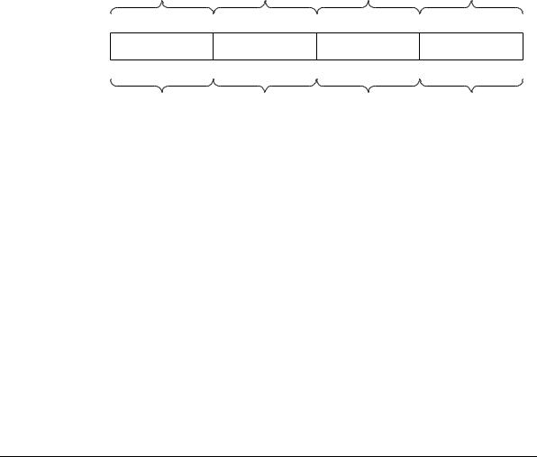
Figure 3-1 on page 3-11 shows the bit assignment for the GPIOPeriphID0-3 registers.
3-10 |
Copyright © 2000 ARM Limited. All rights reserved. |
ARM DDI 0190B |
Programmer’s Model
Actual register bit assignment
Configuration |
|
Revision |
Designer 1 |
Designer 0 |
|
Part |
Part |
|
|||
|
number |
number 1 |
number 0 |
|
|||||||
7 |
0 |
7 |
4 |
3 |
0 |
7 |
4 |
3 |
0 |
7 |
0 |
31 |
24 23 |
20 19 |
16 |
15 |
12 11 |
8 |
7 |
0 |
|||
Configuration |
|
Revision |
|
Designer |
|
|
|
Part number |
|
||
|
|
number |
|
|
|
|
|
|
|
|
|
Conceptual register bit assignment
Figure 3-1 Peripheral identification register bit assignment
Note
When you design a systems memory map you must remember that the PrimeCell GPIO has a 4KB memory footprint. All memory accesses to the peripheral identification registers must be 32-bit, using the LDR and STR instructions.
The four, 8-bit peripheral identification registers are described in the following subsections:
•GPIOPeriphID0 register on page 3-11
•GPIOPeriphID1 register on page 3-12
•GPIOPeriphID2 register on page 3-12
•GPIOPeriphID3 register on page 3-12.
GPIOPeriphID0 register
The GPIOPeriphID0 register is hard coded and the fields within the register determine the reset value. Table 3-12 shows the bit assignment of the GPIOPeriphID0 register.
Table 3-12 GPIOPeriphID0 register
|
Bits |
Name |
Description |
|
|
|
|
|
|
15:8 |
- |
Reserved, read undefined must read as zeros |
|
|
|
|
|
|
|
7:0 |
PartNumber0 |
These bits read back as 0x61 |
|
|
|
|
|
|
|
|
|
|
|
|
ARM DDI 0190B |
Copyright © 2000 ARM Limited. All rights reserved. |
3-11 |
||

Programmer’s Model
GPIOPeriphID1 register
The GPIOPeriphID1 register is hard coded and the fields within the register determine the reset value. Table 3-13 shows the bit assignment of the GPIOPeriphID1 register.
|
|
Table 3-13 GPIOPeriphID1 register |
|
|
|
Bits |
Name |
Description |
|
|
|
15:8 |
- |
Reserved, read undefined, must read as zeros |
|
|
|
7:4 |
Designer0 |
These bits read back as 0x1 |
|
|
|
3:0 |
PartNumber1 |
These bits read back as 0x0 |
|
|
|
GPIOPeriphID2 register
The GPIOPeriphID2 register is hard coded and the fields within the register determine the reset value. Table 3-14 shows the bit assignment of the GPIOPeriphID2 register.
|
|
Table 3-14 GPIOPeriphID2 register |
|
|
|
Bits |
Name |
Description |
|
|
|
15:8 |
- |
Reserved, read undefined, must read as zeros |
|
|
|
7:4 |
Revision |
These bits read back as 0x0 |
|
|
|
3:0 |
Designer1 |
These bits read back as 0x4 |
|
|
|
GPIOPeriphID3 register
The GPIOPeriphID3 register is hard coded and the fields within the register determine the reset value. Table 3-15 shows the bit assignment of the GPIOPeriphID3 register.
|
|
Table 3-15 GPIOPeriphID3 register |
|
|
|
Bits |
Name |
Description |
|
|
|
15:8 |
- |
Reserved, read undefined, must read as zeros |
|
|
|
7:0 |
Configuration |
These bits read back as 0x00 |
|
|
|
3-12 |
Copyright © 2000 ARM Limited. All rights reserved. |
ARM DDI 0190B |
Programmer’s Model
3.3.12PrimeCell identification registers, GPIOPCellID0-3
The GPIOPCellID0-3 registers are four 8-bit wide registers, that span address locations 0xFF0-0xFFC. The registers can conceptually be treated as a 32-bit register. The register is used as a standard cross-peripheral identification system. The GPIOPCellID register is set to 0xB105F00D. Figure 3-2 on page 3-13 shows the bit assignment for the GPIOPCellID0-3 registers.
Actual register bit assignment
GPIOPCellID3 |
|
|
GPIOPCellID2 |
|
GPIOPCellID1 |
|
GPIOPCellID0 |
7 |
0 |
7 |
0 |
7 |
0 |
7 |
0 |
31 |
24 23 |
16 15 |
8 |
7 |
0 |
||
GPIOPCellID3 |
|
|
GPIOPCellID2 |
|
GPIOPCellID1 |
|
GPIOPCellID0 |
Conceptual register bit assignment
Figure 3-2 PrimeCell identification register bit assignment
The four 8-bit PrimeCell identification registers are described in the following subsections:
•GPIOPCellID0 register on page 3-14
•GPIOPCellID1 register on page 3-14
•GPIOPCellID2 register on page 3-14
•GPIOPCellID3 register on page 3-15.
ARM DDI 0190B |
Copyright © 2000 ARM Limited. All rights reserved. |
3-13 |

Programmer’s Model
GPIOPCellID0 register
The GPIOPCellID0 register is hard coded and the fields within the register determine the reset value. Table 3-16 shows the bit assignment of the GPIOPCellID0 register.
|
|
Table 3-16 GPIOPCellID0 register |
|
|
|
Bits |
Name |
Description |
|
|
|
15:8 |
- |
Reserved, read undefined, must read as zeros |
|
|
|
7:0 |
GPIOPCellID0 |
These bits read back as 0x0D |
|
|
|
GPIOPCellID1 register
The GPIOPCellID1 register is hard coded and the fields within the register determine the reset value. Table 3-17 shows the bit assignment of the GPIOPCellID1 register.
|
|
Table 3-17 GPIOPCellID1 register read bits |
|
|
|
Bits |
Name |
Description |
|
|
|
15:8 |
- |
Reserved, read undefined, must read as zeros |
|
|
|
7:0 |
GPIOPCellID1 |
These bits read back as 0xF0 |
|
|
|
GPIOPCellID2 register
The GPIOPCellID2 register is hard coded and the fields within the register determine the reset value. Table 3-18 shows the bit assignment of the GPIOPCellID2 register.
|
|
Table 3-18 GPIOPCellID2 register read bits |
|
|
|
Bits |
Name |
Description |
|
|
|
15:8 |
- |
Reserved, read undefined, must read as zeros |
|
|
|
7:0 |
GPIOPCellID2 |
These bits read back as 0x05 |
|
|
|
3-14 |
Copyright © 2000 ARM Limited. All rights reserved. |
ARM DDI 0190B |

Programmer’s Model
GPIOPCellID3 register
The GPIOPCellID3 register is hard coded and the fields within the register determine the reset value. Table 3-19 shows the bit assignment of the GPIOPCellID3 register.
|
|
Table 3-19 GPIOPCellID3 register read bits |
|
|
|
Bits |
Name |
Description |
|
|
|
15:8 |
- |
Reserved, read undefined, must read as zeros |
|
|
|
7:0 |
GPIOPCellID3 |
These bits read back as 0xB1 |
|
|
|
ARM DDI 0190B |
Copyright © 2000 ARM Limited. All rights reserved. |
3-15 |

Programmer’s Model
3-16 |
Copyright © 2000 ARM Limited. All rights reserved. |
ARM DDI 0190B |