

Brash D.The ARM architecture version 6
.pdfARM White Paper |
January 2002 |
The ARM Architecture Version 6 (ARMv6)
David Brash
Architecture Program Manager, ARM Ltd.
A microprocessor’s architecture defines the instruction set and programmer’s model for any processor that will be based on that architecture. Different processor implementations may be built to comply with the architecture. Each processor may vary in performance and features, and be optimized to target different applications.
Future processors, based on the new ARMv6 architecture will provide developers of embedded systems with higher levels of system performance, whilst maintaining excellent power and area efficiency.
The Evolution of the ARM Architecture
The ARM architecture has evolved steadily to respond to the changing needs of ARM’s partners, and of the design community in general.
At each major revision of the ARM architecture, significant features have been added. Between major architecture revisions, new features have been included as variants on the architectures. The key letters appended to the core names indicate specific architecture enhancements within each implementation.
•V3 introduced 32-bit addressing, and architecture variants: o T – Thumb state: 16-bit instruction execution.
o M – long multiply support (32 x 32 => 64 or 32 x 32 + 64 => 64). This feature became standard in architecture V4 onwards.
•V4 added halfword load and store.
•V5 improved ARM and Thumb interworking, count leading-zeroes (CLZ) instruction, and architecture variants:
o E – enhanced DSP instructions including saturated arithmetic operations and 16-bit multiply operations
o J – support for new Java state, offering hardware and optimized software acceleration of bytecode execution.
All of the ‘TEJ’ enhancements above become part of the new ARMv6 architecture specification.
In order to maintain backwards compatibility, ARMv6 also includes ARMv5 compliant memory management and exception handling. This enables the significant third-party developer community to exploit existing development effort, and supports the reuse of existing software and design experience.
Page 1 of 15 |
© ARM 2002 |
ARM White Paper |
January 2002 |
The introduction of a new architecture does not replace existing architectures, or make them redundant. Where the provisions of ARMv4 or ARMv5 meet market needs, new cores and derivative products will continue to be based on these architectures, whilst tracking technology and process trends. For example, the ARM7TDMI core based on the V4T architecture is still being ‘designed-in’ to many new products, where a performance level of 100MIPS or so is adequate. Processors based on the ARMv5 architecture continue in development.
The ARM architecture will of course continue to evolve with appropriate enhancements in the future.
V7 cores
|
|
|
ARMv7 |
|
|
|
|
|
|
|
V6 cores |
|
|
|
|
|
ARMv6 |
|
|
|
|
|
|
XScaleTM |
ARM1022E |
|
|
|
|
|
|
|
|
|
|
ARMv5 |
|
|
|
|
|
|
|
|
ARM1020 |
ARM926EJ |
|
|
|
ARM7TDMI |
ARM720T |
ARM9E |
ARM10EJ |
|
|
|
|
|
|
|
||
V4 |
|
|
|
|
|
|
|
StrongARM® |
|
ARM920T |
|
|
|
1994 |
1996 |
1998 |
2000 |
2002 |
2004 |
2006 |
time
Figure 1. ARM Architecture Revisions
Implementations of the ARMv6 architecture are primarily driven by ARM’s partner development activity. The first ARM implementations of ARMv6 are underway; more information will be released with the product rollout during 2002.
Driving Architecture Development
Next generation architectures have been driven by the needs of emerging products and evolving markets. The key design constraints are predictable. The function, performance, speed, power, area and cost parameters must be balanced to meet the requirements of each application. ARMv6 offers better ways of optimizing these constraints across a number of vertical market segments.
Delivering leading performance/power (MIPS/Watt) has been fundamental to ARM’s success in the past, and will continue to be a critical benchmark for future applications.
Page 2 of 15 |
© ARM 2002 |
ARM White Paper |
January 2002 |
Functionality is growing dramatically as computing and communications continue to converge in many consumer products. Increasingly, consumers expect features such as advanced user interfaces, multimedia capability and improved product quality. ARMv6 will enable more efficient support for all of these new features and technologies across a number of market segments.
A number of specific market drivers for ARMv6 have been identified. ARMv6 will benefit developers targeting wireless, networking, automotive and consumer entertainment markets. ARM has worked with architecture licensees and key partners such as Intel, Microsoft, Symbian and Texas Instruments in specifying the requirements for ARMv6.
As well as taking into account changing market requirements, key improvements in software, synthesis and process technology also influence the architecture specification. The development of ARMv6 will enable partners to better exploit these, and other technological advances.
Key ARMv6 Improvements
In developing the ARMv6 architecture, effort has been focused on five key areas:
Memory Management
System design and performance is heavily affected by the way that memory is managed. The memory management architectural enhancements improve the overall processor performance significantly – especially for platform-type applications where operating systems need to manage frequent task changes. With the changes in ARMv6, average instruction fetch and data latency is greatly reduced; the processor has to spend less time waiting for instructions or data cache misses to be loaded. The memory management improvements will provide a boost in overall system performance by as much as 30%.
In addition, the memory management enhancements will enable more efficient bus usage. Less bus activity will yield significant power savings as a result of reduced memory access.
Multiprocessing
Application convergence is driving system implementations towards the need for multiprocessor systems. Wireless platforms, especially for 2.5G and 3G, are typical applications that demand integration between ARM processors, ARM and DSPs, or other application accelerators.
Multiprocessor systems share data efficiently by sharing memory. New ARMv6 capabilities in data sharing and synchronization will make it easier to implement multiprocessor systems, as well as improving their performance. New instructions enable more complex synchronization schemes, greatly improving system efficiency.
Page 3 of 15 |
© ARM 2002 |

ARM White Paper |
January 2002 |
Multimedia Support
Single Instruction Multiple Data (SIMD) capabilities enable more efficient software implementation of high-performance media applications such as audio and video encoders. Over sixty SIMD instructions are added to the ARMv6 Instruction Set Architecture (ISA).
Adding the SIMD instructions will provide performance improvements of between 2x and 4x, depending on the multimedia application. The SIMD capabilities will enable developers to implement high-end features such as video codecs, speaker-independent voice recognition and 3D graphics, especially relevant for next generation wireless applications.
Data Handling
A system’s endianism refers to the way data is referenced and stored in a processor’s memory.
With increasing system on a chip (SoC) integration, a single chip is more likely to contain little-endian OS environments and interfaces (such as USB, PCI), but with bigendian data (TCP/IP packets, MPEG streams). With ARMv6, support for mixed-endian systems has been improved. As a result, handling data in mixed-endian systems under ARMv6 is far more efficient.
Unaligned data is data that is not aligned to its natural size boundary. For example, within DSP applications there is sometimes a requirement to treat words with half-word data alignment. For a processor to handle this situation efficiently requires that it be able to load a word aligned to any half-word boundary.
Current versions of the architecture require a number of instructions to manage unaligned data. ARMv6 compliant architectures will manage unaligned data more efficiently in hardware. In algorithms that rely heavily on DSP operations with unaligned data, ARMv6 implementations will have a performance advantage and may also benefit from reduced code size. Unaligned support also makes it more efficient for ARM to emulate other processors, such as Motorola’s 68000 family.
Similar to recent ARMv5 implementations such as ARM10 and XScale1™, ARMv6 is based on a 32-bit processor. ARMv6 will support implementations based on bus widths of 64-bits and above - ARM10 and XScale support 64-bit buses today. This provides bus throughput equivalent to, or even better than a 64-bit machine, but without the power and area overhead of a full 64-bit CPU.
Exceptions and Interrupts
For implementations targeted at real-time systems, efficient handling of interrupts can be critical. Examples include systems such as hard disk controllers, and engine management
1 XScale is a registered trademark of Intel Corporation.
Page 4 of 15 |
© ARM 2002 |
ARM White Paper |
January 2002 |
applications, where the consequences can be severe if a critical interrupt does not get serviced in time. More efficient handling of exception and interrupt conditions also improve overall system performance. This is especially important in reducing system latency.
In ARMv6, new instructions have been added to the ISA to improve the implementation of interrupts and exceptions. These provide the ability to efficiently nest exception handling onto a different privileged mode.
Each of these architectural advances is described in more detail in the following sections.
Programmer’s Model
Six new status bits have been added to the programmer’s model. Four bits are associated with providing “greater than or equal to” status for the new multimedia instructions. The E-bit indicates the current load/store endian setting for the core, and the A-bit is used to mask imprecise data aborts.
•GE[3:0] bits
oSIMD status bits - greater than or equal to for each 8/16-bit slice
•E-bit
oIndicates the current load/store endian setting of the core
oCan be set/cleared with the SETEND instruction
•A-bit
oIndicates if imprecise data abort exceptions are masked
Compatibility
ARMv6 maintains 100% backward compatibility at the binary level for operating systems and applications. The ARMv6 architecture requires that all Thumb and ‘E’ instructions be implemented for backwards compatibility with ARMv5.
Some of the newly introduced ARMv6 instructions also have Thumb equivalents – for example the new ‘REV*’ instructions. The BXJ instruction is also a requirement within ARMv6 for consistent Java support – regardless of whether Jazelle technology is implemented or not.
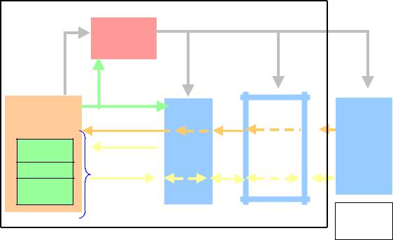
Improved Memory Management
Memory management is primarily concerned with two issues. First, the translation of virtual addresses into physical addresses within a system. Second, ensuring appropriate levels of protection between different processes and tasks.
Page 5 of 15 |
© ARM 2002 |
ARM White Paper |
January 2002 |
The ARM architecture is a load-store architecture, where the ARM core instructions can only operate on data in registers that form part of the core. Load and store instructions are used to transfer data to and from this register file.
A multi-level memory system is part of normal system design hierarchy. Closer coupled memory systems tend to run faster, with level 1 memory systems ideally having no wait states. In practical terms, this limits the size of memories that can be supported at core clock speeds. Many high performance systems are now supporting additional (larger) L2 caches with some wait states, but less latency than if the memory was located off-chip. L3 cache may be provided as fast off-chip SRAM, with "normal" DRAM a level behind that.
ARM first introduced cores (e.g. ARM7TDMI), then developed and offered cached cores with MMU's (e.g. ARM720/920). ARMv6 is a logical progression on this - providing a complete definition of the L1 memory system, and to a lesser extent how memory levels beyond this need to behave for overall system correctness.
Physical Address
Address
Virtual translation
Address
|
CP15 configuration |
|
|
|
|
- control |
|
|
|
ARM core |
Instruction |
Level 1 |
|
|
|
Cache(s) |
Level 2 |
DRAM |
|
|
Prefetch |
|
|
|
|
|
|
SRAM |
|
|
|
Tightly |
|
|
R15 |
|
Cache(s) |
|
|
Load |
Coupled |
Flash |
||
. |
Memory |
|
ROM |
|
. |
|
|
|
|
. |
|
- |
|
|
R0 |
Store |
|
|
|
TCM(s) |
|
|
||
|
|
|
||
|
|
|
|
Additional |
|
|
|
|
Processors |
Figure 2. ARMv6 Memory Model
L1 memory will run synchronized to the core. Where different clock domains are introduced into a design, memory synchronization becomes dependent on the implementation.
Page 6 of 15 |
© ARM 2002 |
ARM White Paper |
January 2002 |
ARM Virtual Memory System Architecture
The ARM Virtual Memory System Architecture v6 (VMSAv6) fully specifies the new Level 1 cache system – that most tightly coupled to the processor. The VMSA also specifies a Tightly-Coupled Memory (TCM) and DMA system. The architecture permits a range of implementations of these systems, with software-visible configuration registers to allow identification of the resources that exist. V6 supports hierarchy and memory ordering rules to ensure system correctness for additional levels of cache in both single processor and multiprocessor systems. Memory ordering rules define the architecture, without constraining the implementation.
Version 6 now supports physically tagged caches, reducing software overhead on context switches. This can save up to 20% of the processor utilization by eliminating the need to perform cache flushing by the OS.
ARM v6 L1 Cache
The L1 cache is architected to reduce the requirement for cache clean and invalidation on a context switch. The cache may be organized as a Harvard system with separate instruction and data caches, or as a single unified von Neumann cache. The TCM is a physically-addressed area of scratchpad memory, which is implemented alongside the L1 cache. Similarly, the TCM can be organized as a Harvard or von Neumann system. The L1 DMA subsystem is designed to allow background transfers to and from the TCM.
Page Table Formats
Page table formats have been revised in ARMv6. Figure 3 illustrates the new first level page table format.
|
|
|
SBZ |
|
|
|
|
|
0 |
0 |
|||
|
|
|
|
|
|
|
|
|
|
|
|
|
|
Coarse page table page address |
P |
Domain |
|
SBZ |
0 |
1 |
|||||||
|
|
|
|
|
|
|
|
|
|
|
|
|
|
|
|
|
|
A |
|
|
|
|
|
|
|
|
|
Section base address |
SBZ |
nG |
S |
P |
TEX |
AP |
P |
Domain |
XN |
C |
B |
1 |
0 |
|
|
|
|
X |
|
|
|
|
|
|
|
|
|
|
|
|
|
|
|
|
|
|
|
|
|
|
|
|
|
Reserved |
|
|
|
|
|
1 |
1 |
||||
|
|
|
|
|
|
|
|
|
|
|
|
|
|
Figure 3. ARMv6 First Level Page Table Format
The XP bit in Coprocessor 15 is used to enable this format, otherwise an ARMv5 legacy mode is invoked for backwards compatibility.
New features include:
•an execute never bit (XN)
•a “not Global” (nG) bit for address matching
Page 7 of 15 |
© ARM 2002 |
ARM White Paper |
January 2002 |
Application Space Identifier - or ASID - support is another key feature in this area. When the nG-bit is set, address translation uses the virtual address and ASID for translation matching. This provides a significant saving in software overhead on context switches, avoiding the need to flush on-chip translation buffers in most cases. The result is improved performance. The architecture also supports its use in task-aware debugging. The ASID forms part of a process ID that can be used in task aware debugging.
Type extension, shared, and access permission bits are used to provide all the attributes necessary for the ARMv6 memory model. A P-bit, which is compatible with the mechanism already available on Intel’s XScaleTM product, has been added for memory protection.
Additional Translation Table Base Register
To improve page table handling, a second translation table base register has been added; CP15 now supports TTBR0 and TTBR1. A control register is used to program N, the number of leading zeroes (most significant address bits) in virtual addresses that use TTBR0; 0 < N < 7. The device resets with N equal to zero, meaning all virtual addresses use TTBR0, otherwise the address space 0-232-N will use TTBR0 and other addresses will use TTBR1. The size of the first level page table required for TTBR0 will vary from 128 bytes to 16kB depending on the value of N, offering additional scope for memory savings in resource critical systems, particularly where multiple tables are held in memory and swapped on a context switch by updating the translation base register.
Multiprocessing
While many ARM processors today are used in isolation, or with simple communications links to another resource with its own memory, there are increasing requirements for unified memory models, and closer coupling of processors in general.
Systems consisting of multiple processors – either multiple ARM processors or a mixture of ARMs and DSPs, are becoming more common. Improvements to the ARMv6 memory management unit (MMU) are important in ensuring that processors get predictable and consistent (coherent) views of memory when it is shared between multiple processors.
Improvements include defining the level1 memory system, and the memory order model - how loads and stores to memory relate to each other.
As well as memory improvements to facilitate multiprocessing, Load and Store Exclusive instructions have been added in version 6 to support semaphores in multiprocessor systems (used to synchronise tasks). These instructions provide a more powerful and flexible mechanism over the current swap instructions.
•LDREX{<cond>} <Rd>, [<Rn>]
This performs a load, then sets a monitor to “watch” the address
•STREX {<cond>} <Rd>, <Rm>, [<Rn>]
This performs a store and returns “success” in Rd if no intervening access detected by the monitor.
Page 8 of 15 |
© ARM 2002 |
ARM White Paper |
January 2002 |
Exceptions and Interrupts
The desire to implement more efficient processing of exception and interrupt conditions has led to several architectural enhancements in ARMv6. A low interrupt latency mode allows implementations to modify or switch off features. This is enabled by the FI bit in CP15 register 1 (the CPU control and configuration register). This facility enables designers to make performance versus latency tradeoffs, and support both in the design. For example, Load Multiple or Store Multiple instructions (LDM/STM) can be made interruptible where low latency is important. Normally, these instructions would run to completion.
ARMv6 provides for vectored interrupt support. The Vectored Interrupt Controller (VIC) is enabled by the VE bit in CP15 register 1. The VE bit is used to enable returning vectored interrupts directly to the core. VIC support is currently provided through an external system peripheral. This requires an IRQ or FIQ system interrupt, and then the interrupt handler needs to perform a memory mapped read of a register for the vector address.
Imprecise external aborts are supported in ARMv6. The A-bit added to the program status register (CPSR), provides an abort mask for this - like the I and F bit masks for IRQ and FIQ.
Stack Handling and Mode Change support
New stack handling capabilities in ARMv6 avoid the need for multiple stacks. The ARMv6 register model supports separate stacks in the different modes. Many operating systems like to nest all their state saving and restoring onto a single stack. Version 6 makes this much more efficient. The stack handling capabilities are based on new crossmode state-saving instructions:
•SRS #Mode - Save Return State onto stack belonging to ‘Mode’
•RFE - Return From Exception
The SRS instruction allows register 14 and the SPSR (Saved Processor Status Register) for the current mode to be saved to a stack in a different mode. The RFE instruction loads the PC and CPSR (Current Processor Status Register) from the saved state.
New instructions support fast mode changes in privileged modes. Instructions cannot be used in user mode for security reasons.
•CPSID #Mode (and disable interrupts)
•CPSIE #Mode (and enable interrupts)
The CPS instructions allow software to move efficiently to a different mode while enabling or disabling interrupts.
Page 9 of 15 |
© ARM 2002 |

ARM White Paper |
January 2002 |
Table 1a and 1b show code extracts, including entry code and exit code, comparing stack handling with SRS/CPS/RFE usage in ARMv6 with ARMv5. The two sections of code are exact equivalents for the context:
•An FIQ entry - FIQ2 - from a VIC is to be processed in ABORT mode (there is a higher priority FIQ - FIQ1 - which uses FIQ mode directly)
•In ARMv5, the handler needs to use the FIQ_stack as a scratchpad for R0-R3 to provide the necessary workspace
•The target (abort mode) stack has R2, R3, R14 (Link register) and SPSR (the saved status captured in FIQ mode needed for the eventual return) added to the ABORT_stack
•R0 and R1 are transferred with their context intact
ARMv5 |
ARMv6 |
FIQ2handler. FIQs are now re-enabled, with original R2, R3, R14, SPSR on stack. Includes code to stack any more registers required, process the interrupt and unstack extra registers.
STMIA |
|
R13, {R0-R3} |
|
SUB |
R14, R14, #4 |
MOV |
|
R0, LR |
|
SRSFD |
R13_abt! |
MRS |
|
R1, SPSR |
|
CPSIE |
f, #0x1B ; = Abort mode |
ADD |
|
R2, R13, #8 |
|
STMFD |
R13!, {R2,R3} |
MRS |
|
R3, CPSR |
|
|
|
BIC |
R3, R3, #0x1F |
|
|
|
|
ORR |
|
R3, R3, #0x1B |
; = Abort mode No. |
|
|
MSR |
|
CPSR_c, R3 |
|
|
|
STMFD |
R13!, {R0,R1} |
|
|
||
LDMIA |
|
R2, {R0,R1} |
|
|
|
STMFD |
R13!, {R0,R1} |
|
|
||
LDMDB |
R2, {R0,R1} |
|
|
|
|
BIC |
R3, R3, #0x40 |
; = F bit |
|
|
|
MSR |
|
CPSR_c, R3 |
|
|
|
|
|
||||
Exit code including the LDR/STR instructions needed to acknowledge the VIC |
|||||
ADR |
|
R2, #VICaddress |
LDMFD |
R13!, {R2,R3} |
|
MRS |
|
R3, CPSR |
|
ADR |
R14, #VICaddress |
ORR |
|
R3, R3, #0x40 |
; = F bit |
CPSID |
f |
MSR |
|
CPSR_c, R3 |
|
STR R0, [R14,#AckFinished] |
|
STR |
R0, [R2,#AckFinished] |
RFEFD |
R13! |
||
LDR |
R14, [R13,#12] |
; Original SPSR value |
|
|
|
MSR |
|
SPSR_fsxc, R14 |
|
|
|
LDMFD |
R13!, {R2,R3,R14} |
|
|
||
ADD |
|
R13, R13, #4 |
|
|
|
SUBS |
|
PC, R14, #4 |
|
|
|
|
|
|
|||
Approximate cycles: 35 |
|
Approximate cycles: 11 |
|||
|
|
|
Table 1a. Efficient code handling in ARMv6 |
||
The code illustrates a different stack mechanism for FIQ-mode and ABORT-mode:
•FIQ-mode: "Empty ascending" stack; uses STMIA and LDMDB
Page 10 of 15 |
© ARM 2002 |