

Davis W.A.Radio frequency circuit design.2001
.pdf160 NOISE
GATE
SOURCE |
|
|
|
|
|
|
|
|
|
SOURCE |
|
|
|
|
|
|
|
|
|
||
|
|
|
|
|
|
|
|
|
||
|
|
|
|
|
|
|
|
|
|
|
|
|
|
|
|
|
|
|
|
|
|
|
|
|
|
|
|
|
|
|
|
|
DRAIN
FIGURE 8.8 Typical FET layout.
These circuit elements can clearly be adjusted by scaling the transistor geometry. This scaling will in turn change the noise characteristics. If a transistor with a given geometry has a known set of noise parameters, then the noise characteristics of a new modified transistor can be predicted. The scaling factors between the new and the old transistor are
W0
s1 D
W W0/N0
s2 D
W/N
As a result the new equivalent circuit parameters can be predicted [11]:
g0m D gms1
Rs0 D Rs s1
Rd0 D Rd s1
C0gs D Cgss1
Rg0 D Rgs2
8.74
8.75
8.76
8.77
8.788.79

PROPERTIES OF CASCADED AMPLIFIERS |
161 |
The Fukui equations, (8.70) to (8.73), for the newly scaled equivalent circuit parameters are given as follows:
|
|
|
|
|
|
|
|
|
|
Rg0 |
C Rs0 |
1/2 |
|
|
|
F0 |
D |
1 |
C |
k |
fC0 |
|
|
|
|
||||||
|
|
gm0 |
|
|
|
||||||||||
min |
|
|
1 |
|
gs |
|
|
|
|
|
|||||
|
|
|
|
|
|
|
|
|
|
|
|
s1s2Rg C Rs |
1/2 |
||
|
D |
1 |
C |
F |
min |
1 |
|
8.80 |
|||||||
|
|
Rg C Rs |
|||||||||||||
|
|
|
|
|
|
|
|
|
|||||||
Rn0 |
D |
Rn |
|
|
|
|
|
|
|
|
|
8.81 |
|||
s1 |
|
|
|
|
|
|
|
|
|
|
|||||
R0 |
|
|
Ropt |
|
1 C 4gm Rs C Rgs1s2 |
|
8.82 |
||||||||
D s1 |
|
|
|||||||||||||
opt |
|
|
1 C 4gm Rs C Rg |
|
|||||||||||
Xopt0 |
D |
|
Xopt |
|
|
|
|
|
|
|
|
|
8.83 |
||
|
|
s1 |
|
|
|
|
|
|
|
|
|
||||
Reference should be made to [11] for a much fuller treatment of modeling MESFETs and HEMTs.
The bipolar transistor has a much different variation of noise with frequency than does the FET type of device. An approximate value for Fmin for the bipolar transistor at high frequencies is [12]
|
|
|
|
2 |
|
|
Fmin ³ 1 C h 1 C |
1 C |
|
8.84 |
|||
h |
||||||
where |
|
|
|
2 |
|
|
qIcrb |
|
ω |
|
8.85 |
||
h D |
|
|
|
|
|
|
kT |
|
ωT |
|
|
||
In this equation, Ic is the dc collector current, rb is the base resistance, and ωT is the frequency where the short circuit current gain is 1. Values for Yopt and Rn are also given in [12] but are rather lengthy. A somewhat more accurate expression is given in [13].
Comparison of Eq. (8.84) with the corresponding expression for FETs, Eq. (8.70), indicates that the bipolar transistor minimum noise figure increases with f2, while that for the FET increases only as f. Consequently designs of low-noise amplifiers at RF and microwave frequencies would tend to favor use of FETs.
8.10PROPERTIES OF CASCADED AMPLIFIERS
Ideally amplifiers are completely unilateral so that there is no feedback signal returning to the input side. Under this condition analysis of cascaded amplifiers

162 NOISE
results in some interesting properties related to noise figure and efficiency. The results obtained will be approximately valid for almost unilateral amplifiers, even if some of the “amplifiers” are attenuators. The following two sections deal with the total noise figure and total efficiency respectively of a cascade of unilateral amplifiers.
8.10.1Friis Noise Formula
The most critical part for achieving low noise in a receiver is the noise figure and gain of the first stage. This is intuitively clear, since the magnitude of the noise in the first stage will be a much larger percentage of the incoming signal than it will be in subsequent stages where the signal amplitude is much larger. For a receiver with n unilateral stages, the total noise figure for all n stages is [14]
NTn |
8.86 |
FTn D kT0 fG1G2 . . . Gn |
where NTn is the total noise power delivered to the load. This can be expressed in terms of the sum of the noise added by the last stage, Nn, and that of all the previous stages multiplied by the gain of the last stage:
NTn D Nn C GnNT n 1 |
8.87 |
If the nth stage were removed, and its noise figure measured alone, then its noise figure would be
F |
n D |
kT0Gn f C Nn |
8.88 |
|||
kT0Gn f |
||||||
|
|
|||||
or |
|
|
Nn |
|
||
Fn 1 D |
8.89 |
|||||
kT0Gn f |
|
|||||
By substituting Eq. (8.87) into Eq. (8.86) an expression for the noise figure is obtained that separates the contributions of the noise coming from the last stage only from the previous n 1 stages:
FTn D |
|
|
Nn |
|
C |
GnNT n 1 |
8.90 |
|
kT0 fGn G1G2 . . . Gn 1 |
kT0 fG1G2 . . . Gn 1Gn |
|
||||||
Canceling the Gn in the second term and substituting Eq. (8.89) yields |
|
|||||||
|
F |
|
Fn 1 |
|
|
NT n 1 |
|
8.91 |
|
Tn D G1G2 . . . Gn 1 |
C kT0 fG1G2 . . . Gn 1 |
||||||
|
|
|
||||||
The second term in Eq. (8.91) is the same as Eq. (8.86) except that n has been reduced to n 1. This process is repeated n times giving what is known as the

PROPERTIES OF CASCADED AMPLIFIERS |
163 |
Friis formula for the noise figure for a cascade of unilateral gain stages:
F |
|
F |
|
F2 1 |
|
F3 1 |
|
Fn 1 |
8.92 |
|
Tn D |
C |
G1 |
C G1G2 |
C Ð Ð Ð C G1G2 . . . Gn 1 |
||||||
|
1 |
|
||||||||
Clearly the noise figure of the first stage is the most important contributor to the overall noise figure of the system. If the first stage has reasonable gain, the subsequent stages can have much higher noise figure without affecting the overall noise figure of the receiver.
8.10.2Multistage Amplifier Efficiency
For a multistage amplifier, the overall power efficiency can be found that will correspond in some way with the overall noise figure expression. Unlike the noise figure, however, the efficiency of the last stage will be found to be most important. Again, this would appear logical since the last amplifying stage handles the greatest amount of power so that poor efficiency here would waste the most amount of power. For the kth stage of an n stage amplifier chain, the power added efficiency is
, |
k D |
Pok Pik |
8.93 |
|
Pdk |
||||
|
|
where
Pok D output power of the kth stage Pik D input power to the kth stage
Pdk D source of power which is typically the dc bias for the kth stage
If the input power to the first stage is Pi1, then |
|
Pik D Pi1G1G2G3 . . . Gk 1 |
8.94 |
and for the kth stage alone |
|
Pok D PikGk |
8.95 |
When Eq. (8.94) and Eq. (8.95) are substituted into the efficiency equation, Eq. (8.93), the power from the power source can be found:
P |
G1G2 . . . Gk 1 Gk 1 |
P |
|
8.96 |
dk D |
,k |
i1 |
|
|
The total added power for a chain of n amplifiers is |
|
|
||
Pon Pi1 D Pi1 G1G2G3 . . . Gn 1 |
8.97 |
|||
The efficiency for the whole amplifier chain is clearly given by the following:
, |
T D |
Pon Pi1 |
8.98 |
|
n |
||||
|
|
Pdk
iD1

164 NOISE
Replacing the power levels in Eq. (8.98) with their explicit expression gives the value for the overall efficiency of a chain of unilateral amplifiers:
, |
|
|
|
|
|
|
|
G1G2G3 . . . Gn 1 |
|
|
8.99 |
||
T D G1 |
1 G1 |
G2 |
|
G1G2 . . . Gn 1 Gn 1 |
|||||||||
|
1 |
|
|
||||||||||
|
|
,1 |
C |
|
,2 |
|
C Ð Ð Ð C |
|
,n |
|
|
||
When each amplifier stage has a gain sufficiently greater than one, the overall efficiency becomes
,T ³ |
|
1 |
|
8.100 |
1 |
1 |
1 |
C Ð Ð Ð C C
G2G3 . . . Gn,1 Gn,n 1 ,n
This final equation illustrates that it is important to make the final stage the most efficient one
8.11AMPLIFIER DESIGN FOR OPTIMUM GAIN AND NOISE
The gain for a nonunilateral amplifier was previously given as Eq. (7.15) is repeated here:
G |
|
jS21j2 1 j Gj2 1 j Lj2 |
8.101 |
|
T D j 1 GS11 1 LS22 S12S21 G Lj2 |
||||
|
|
|||
If S12 is set to zero, thereby invoking the unilateral approximation for the amplifier gain, then
G |
|
1 j Gj2 |
S |
21j |
2 |
1 j Lj2 |
8.102 |
|
|
|
j 1 LS22j2 |
||||
|
T ³ j1 GS11j2 j |
|
|
||||
This approximation of course removes the possibility of analytically determining the transistor stability conditions. Using this expression, a set of constant gain circles can be drawn on a Smith chart for a given transistor. That is, for a given set of device scattering parameters and for a fixed load impedance, a set of constant gain circles can be drawn for a range of generator impedances expressed here in terms of G.
The noise figure was previously found in Eq. (8.40). As was done for the constant gain circles, constant noise figure circles can be drawn for a range of values for the generator admittance, YG D GG C jBG. The optimum gain occurs when G D S11Ł , and the minimum noise figure occurs when YG D Yopt. These two source impedances are rarely the same, but a procedure is available that at least optimizes both of these parameters simultaneously [15]. As seen on the Smith chart in Fig. 8.9, it appears that the least damage to either the gain or the noise figure is obtained if the actual chosen generator impedance lies on a

AMPLIFIER DESIGN FOR OPTIMUM GAIN AND NOISE |
165 |
FIGURE 8.9 Constant gain and noise figure circles.
Input |
Output |
Match |
Match |
Circuit |
Circuit |
FIGURE 8.10 Series inductive feedback can be used to lower noise figure.
line between S11Ł and Yopt. It has been found that addition of series inductance, such as shown in Fig. 8.10, will lower the minimum noise figure of the circuit because it lowers the effective Fmin and rn. This series inductance also increases the real part of the input impedance. The output impedance does not affect the noise figure, but it can be manipulated to adjust the gain.
166 NOISE
R L
+
< v 2 >
–
FIGURE 8.11 Noise current developed by a series RL circuit.
PROBLEMS
8.1What is the noise voltage at the output of Fig. 8.2 when the capacitor is removed from the circuit?
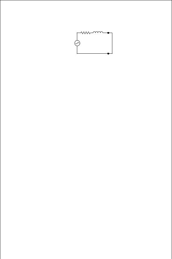
8.2What is the noise current from a noise voltage source in a series RL circuit shown in Fig. 8.11.
8.3Derive Eqs. (8.80) to (8.83).
8.4 A MESFET has a base width W D 300 m and at 2 GHz with a given bias is found to have gm D 75 mS, Rg D 1 -, Rd D 5 -, Rs D 3 -, and Cgs D 0.4 pF. What are the four noise parameters Fmin, Rn, Ropt, and Xopt? If the base width is changed to W0 D 200 m and the number of base fingers remains unchanged, what are the four noise parameters?
8.5A three-stage amplifier consists of three individual unilateral amplifiers. The first one (the input stage) has a gain G1 D 10 dB, a noise figure F1 D 1.5, and an efficiency ,1 D 1%. For stage 2, G2 D 20 dB, F2 D 10, and ,2 D 5%. For stage 3, G3 D 5 dB, F3 D 15, and ,3 D 50%. What is the overall total noise figure for the cascaded amplifier? What is the overall total efficiency for the cascaded amplifier?
REFERENCES
1.J. L. Plumb and E. R. Chenette, “Flicker Noise in Transistors,” IEEE Trans. Electron Devices, Vol. 10, pp. 304–308, 1963.
2.A. Messiah, Quantum Mechanics, Amsterdam: North-Holland 1964, ch. 12.
3.W. A. Davis, Microwave Semiconductor Circuit Design, New York: Van Nostrand, 1984, chs. 8, 9.
4.A. E. Siegman, “Zero-Point Energy as the Source of Amplifier Noise,” Proc. IRE, Vol. 49, pp. 633–634, 1961.
5.H. Nyquist, “Thermal Agitation of Electronic Charge in Conductors,” Physical Rev., Vol. 32, p. 110, 1928.
6.K. Kurokawa, “Actual Noise Measure of Linear Amplifiers,” Proc. IRE, Vol. 49, pp. 1391–1397, 1961.
7.H. A. Haus, “IRE Standards on Methods of Measuring Noise in Linear Twoports,” Proc. IRE, Vol. 47, pp. 66–68, 1959.

REFERENCES 167
8. H. Rohte and W. Danlke, “Theory of Noisy Fourpoles,” Proc. IRE, Vol. 44,
pp. 811–818, 1956.
9.H. A. Haus, “Representation of Noise in Linear Twoports,” Proc. IRE, Vol. 48,
pp. 69–74, 1960.
10.H. Fukui, “Design of Microwave GaAs MESFETs for Broad-Band Low-Noise Amplifiers,” IEEE Trans. Electron Devices, Vol. 26, pp. 1032–1037, 1979.
11.J. M. Golio, Microwave MESFETs and HEMTs, Norwood, MA: Artech House, 1991, ch. 2.
12.H. Fukui, “The Noise Performance of Microwave Transistors,” IEEE Trans. Electron Devices, Vol. 13, pp. 329–341, 1966.
13.R. J. Hawkins, “Limitations of Nielsen’s and Related Noise Equations Applied to Microwave Bipolar Transistors, and a New Expression for the Frequency and Current Dependent Noise Figure,” Solid State Electronics, Vol. 20, pp. 191–196, 1977.
14.H. T. Friis, “Noise Figures of Radio Receivers,” Proc. IRE, Vol. 32, pp. 419–422, 1944.
15.R. E. Lehmann and D. D. Heston, “X-Band Monolithic Series Feedback LNA,” IEEE Trans. Microwave Theory Tech., Vol. 33, pp. 1560–1566, 1985.

Radio Frequency Circuit Design. W. Alan Davis, Krishna Agarwal
Copyright 2001 John Wiley & Sons, Inc.
Print ISBN 0-471-35052-4 Electronic ISBN 0-471-20068-9
CHAPTER NINE
RF Power Amplifiers
9.1TRANSISTOR CONFIGURATIONS
Earlier in Chapter 7, class A amplifiers were treated. Some discussion was given to its application as a power amplifier. While class A amplifiers are used in power applications where linearity is of primary concern, they do so at the cost of efficiency. In this chapter a description of power amplifiers that provide higher efficiency than the class A amplifier. Before describing these in detail, it should be recalled that a single transistor amplifier can be installed in one of four different ways: common emitter, common base, common collector (or emitter follower), and common emitter with emitter degeneracy. Although there are always exceptions, the common emitter circuit is used in amplifiers where high voltage gain is required. The common base amplifier is used when low input impedance and high output impedance is desired. This is accompanied with a current gain ³ 1. The emitter follower is used when high-input impedance and low-output impedance is desired. This is accompanied with a voltage gain ³ 1. The common emitter with emitter degeneracy is used when improved stability is needed with respect to differences in the transistor short circuit current gain (ˇ) with some degradation in the voltage gain. These are illustrated in Fig. 9.1 in which the bias supplies are not shown. These properties are described in detail in most electronics texts.
The transistor itself can be in one of four different states: saturation, forward active, cutoff, and reverse active. It is in the forward active region, when for the bipolar transistor, the base–emitter junction is forward biased and the base– collector junction is reverse biased. These states are illustrated in Fig. 9.2 for a npn transistor. An actual bipolar transistor requires a base–emitter voltage greater than 0.6 to 0.7 volts for it to go into the active state.
The voltage swing of a class A amplifier will remain in the forward active region throughout its entire cycle. If the signal current is given as follows:
io ωt D IOC sin ωt |
9.1 |
168
|
|
|
|
|
|
|
|
|
|
|
|
|
|
|
|
|
|
|
|
THE CLASS B AMPLIFIER |
169 |
|||||||||
|
|
|
|
|
|
|
|
|
|
|
|
|
|
|
|
|
|
|
|
|
|
|
|
|
|
|
|
|
|
|
|
|
|
|
|
|
|
|
|
|
|
|
|
|
|
|
|
|
|
|
|
|
|
|
|
|
|
|
|
|
|
|
|
|
|
|
|
|
|
|
|
|
|
|
|
|
|
|
|
|
|
|
|
|
|
|
|
|
|
|
|
|
|
|
|
|
|
|
|
|
|
|
|
|
|
|
|
|
|
|
|
|
|
|
|
|
|
|
|
|
|
|
|
|
|
|
|
|
|
|
|
|
|
|
|
|
|
|
|
|
|
|
|
|
|
|
|
|
|
|
|
|
|
|
|
|
|
|
|
|
|
|
|
|
|
|
|
|
|
|
|
|
|
|
|
|
|
|
|
|
|
|
|
|
|
|
|
|
|
|
|
|
|
|
|
|
|
|
|
|
|
|
|
|
|
|
|
|
|
|
|
|
|
|
|
|
|
|
|
|
|
|
|
|
|
|
|
|
|
|
|
|
|
|
|
|
|
|
|
|
|
|
|
|
|
|
|
|
|
|
|
|
|
|
|
|
|
|
|
|
|
|
|
|
|
|
|
|
|
|
|
|
|
|
|
|
|
|
|
|
|
|
|
|
|
|
|
|
|
|
|
|
|
|
|
|
|
|
|
|
|
|
|
|
|
|
|
|
|
|
|
|
|
|
|
|
|
|
|
|
|
|
|
|
|
|
|
|
|
|
|
|
|
|
|
|
|
|
|
|
|
|
|
|
|
|
|
|
|
|
|
|
|
|
|
|
|
|
|
|
|
|
|
|
|
|
|
|
|
|
|
(a) Common |
(b) Common |
(c) Emitter |
(d ) Emitter |
Emitter |
Base |
Follower |
Degeneracy |
FIGURE 9.1 (a) Common emitter, (b) common base, (c) common collector or emitter follower, and (d) common emitter with emitter degeneracy.
VBC
I – Saturation
IV |
I |
II – Forward Active
VBE III – Cut Off
IV – Reverse Active
III |
II |
FIGURE 9.2 The four bias regions for a npn bipolar transistor.
and the dc bias current is Idc, then the total instantaneous current is
Idc C IOC sin ωt |
9.2 |
For the class A amplifier, IOC < IC, so the entire waveform of the ac signal is amplified without distortion. The conduction angle is 360°. For the amplifiers under consideration in this chapter, the transistor(s) will be operating during part of their cycle in either cutoff or saturation, or both.
9.2THE CLASS B AMPLIFIER
The class B amplifier is biased so that the transistor is on only during half of the incoming cycle. The other half of the cycle is amplified by another transistor so that at the output the full wave is reconstituted. This is illustrated in Fig. 9.3. While each transistor is clearly operating in a nonlinear mode, the total input wave is directly replicated at the output. The class B amplifier is therefore classed as a linear amplifier. In this case the bias current, IC D 0. Since only one of the