

Interfacing sensors and signal processing components
.pdfSensors - May 1998 - Interfacing Sensors |
and Signal Processing Components |
21/08/2002 09:00 |
Interfacing Sensors
and Signal Processing Components
Most voltage signals produced by sensors require signal processing before they can be converted to digital form or used to drive actuators. To avoid introducing errors into the data, a designer should be aware of problems and techniques common to interfacing sensors with signal processing components.
Ed Ramsden, Cherry Electrical Products
any sensors provide a voltage output in response to a detected phenomenon. Most of these devices, though, don't produce signals strong
enough to be fed directly into an A/D converter or to drive indicators or actuators. To remedy this, analog signal processing often has to boost the sensor's output.
Thevanin-Equivalent Model
Voltage-output transducers measure a variety of effects, but their electrical interfaces can be roughly modeled by an ideal voltage source in series with
Figure 1. A transducer that provides a single voltage output can be modeled as a voltage source Vo in series with a resistor Ro. This approximation is called a Thevanin-equivalent circuit. Ro is commonly called the sensor's output impedance, and Vo is the sensor's zero-load output voltage.
an impedance (see Figure 1). Even though the impedance can result from capacitance or inductance (and vary with signal frequency), it can still be considered a simple resistance for many back-of-envelope calculations.
Impedance limits the energy the signal source can deliver to a load. The same effect prevents you from starting your car's engine with 8 AA batteries in series
http://www.sensorsmag.com/articles/0598/sig0598/main.shtml |
Página 1 de 10 |

Sensors - May 1998 - Interfacing Sensors |
and Signal Processing Components |
21/08/2002 09:00 |
(1.5 V each), even though the total voltage is the same as that of an automobile battery. The difference is that the equivalent resistance of the AA batteries is several orders of magnitude higher than that of the car battery, limiting the peak current they can deliver to a few amperes, as opposed to the several hundred amperes provided by a car battery.
Although few sensors must deliver amperes of current, many have high output impedances (i.e., >106  ) and are easy to improperly load. In the
Figure 2. The inputs to amplifier stages can also be modeled as Thevanin-equivalent circuits. You generally want to use an amplifier with an input impedance much higher than the sensor's output impedance to reduce system gain errors.
case of a sensor output, a Thevanin equivalent circuit can describe the input to an amplifier or other interface circuit.
Figure 2 shows a sensor and an amplifier. The addition of the amplifier has two effects on the output of the sensor. First, the input impedance of the amplifier forms a voltage divider with the output impedance of the sensor, reducing the sensor's output voltage by:
The second effect is caused by the amplifier's bias current (input current source). Although this current is often in the nanoamp or picoamp range, it can cause input offset voltage errors of several millivolts for a sensor with sufficiently high output impedance (Ibias x Rs).
The lesson to be learned here is to select amplifiers with impedances much higher than those of the sensors you are going to use. Also, make sure the amplifiers have bias currents low enough to avoid creating unacceptable input offset errors.
Although the notion of matching input and output impedances is common in the RF, video, and audio worlds, it's usually neither necessary nor desirable for low-frequency signals (i.e., <1 kHz ) that are carried over distances of a few meters or less. In most cases, the DC gain and offset errors caused by attempting to match an amplifier input impedance with a sensor output impedance (which can be highly variable anyhow) will far exceed the AC errors caused by mismatched impedances among sensor, interconnecting cable, and a high-impedance amplifier.
http://www.sensorsmag.com/articles/0598/sig0598/main.shtml |
Página 2 de 10 |

Sensors - May 1998 - Interfacing Sensors |
and Signal Processing Components |
21/08/2002 09:00 |
Single-Ended vs. Differential Measurements
A single voltage sensor output with respect to ground is called a single-ended output; transducers that provide two outputs, where the second either remains constant or changes with an opposite polarity to the first, produce differential or balanced outputs. Single-ended outputs have the advantage of simplicity, but they are more susceptible to interference and signal degradation than differential outputs. In cases where the sensor signal is small and rides
Figure 3. The differential output temperature sensing bridge shown in (B) provides many measurement advantages over the single-ended sensor of (A). It allows for easier measurement of small changes and in most cases will provide a better SNR.
on a significant DC bias, a balanced output lets you more easily discriminate changes, especially when the DC bias changes in response to environmental factors, such as temperature.
Figure 3 shows two thermistor-based temperature-sensing schemes; one is single-ended, and the other is differential. The differential scheme allows for an order of magnitude or more of sensitivity with the same voltmeter because most of the voltmeter's dynamic range isn't consumed in measuring the bias voltage level, as it is in a single-ended measurement.
Because differential measurement schemes are popular, single-IC instrumentation amplifiers (see "Instrumentation Amplifiers: A Tutorial," Sensors, September 1997) are available to amplify differential signals and convert them to single-ended signals for subsequent processing.
Ground and Isolation
Ground is the point at which the voltage is taken to be zero. Unfortunately, voltage levels at one ground are not always the same as they are at another, and this is where the problems begin. Ground variations (measured at the wall outlet) of a few tens of millivolts AC (60 Hz) are not uncommon in the same building. Such small variations don't often present major safety issues, but they can make remote voltage measurements difficult.
One approach is to make sure that the sensor being measured is grounded only at the amplifier inputs. For passive sensors (i.e., those requiring no external power to operate), the signal lead and the return can be brought straight to the amplifier. For active sensors, the technique is more difficult to use because voltage drops along the return lead can lift the ground at the sensor millivolts or even volts above the ground at the amplifier inputs.
http://www.sensorsmag.com/articles/0598/sig0598/main.shtml |
Página 3 de 10 |

Sensors - May 1998 - Interfacing Sensors |
and Signal Processing Components |
21/08/2002 09:00 |
You can avoid the problem by using a differential output sensor, which will cancel out a few hundred millivolts of sensor ground error. For single-ended
Figure 4. Remote sensing lets you avoid offset errors caused by ground shifts on long cable runs. By subtracting the ground potential at the sensor from the sensor's output signal, you can obtain a true output value.
sensors, a technique called remote ground sensing can be used (see Figure 4). By measuring the ground at the sensor and subtracting that value from the sensor output signal (using an instrumentation amplifier), you can obtain the true sensor output. This technique works because there is no voltage drop along wires that don't carry current, which is the case for the sensor output and ground sense leads if the instrumentation amplifier has sufficiently high input impedance and low input bias current.
Sometimes the difference in ground from the beginning of the measurement chain to its end is tens or hundreds of volts. In cases like these, simple differential or ground-sensing schemes won't yield effective results, and in many cases, using these schemes can damage the measuring equipment or injure the people operating it.
A technique called isolation often provides a way to bridge large differences in ground levels. The technique uses devices known as isolators, which allow signal levels to be communicated from their inputs to their outputs, but which have no electrical connection between the two. Isolators typically use an optical, magnetic, or capacitive bridge between the inputs and the outputs (see Figure 5). The input signal is converted to a proportional duty-cycle pulse stream, which is used to drive an LED. A photodiode on the output side of the isolator receives the optical pulses from the LED and outputs an electrical pulse stream that is then low-pass filtered.
Figure 5. An isolator allows communication of signal values between two circuits with no electrical connection. The input signal is modulated onto a carrier, sent across the isolation barrier-in this case optically-and then demodulated on the other side. Optical, capacitive, and magnetic technologies are all commonly used to implement isolators.
http://www.sensorsmag.com/articles/0598/sig0598/main.shtml |
Página 4 de 10 |

Sensors - May 1998 - Interfacing Sensors |
and Signal Processing Components |
21/08/2002 09:00 |
In addition to protecting the measurement device from the system being measured, isolation is also used to protect the system being measured from the measurement device, particularly in medical applications. Isolation between a patient and medical instrumentation helps ensure that the patient will not be injured or killed by electric shock in the event of a malfunction or grounding problem with the instrument.
Low-Voltage Signals
Transducers often output microvolt signals, and you encounter difficulties when you try to accurately measure such small signals. The major difficulties are intrinsic noise from the sensor and the amplifier, thermal errors, and EMI.
Electronic devices produce electrical noise, and these noise sources set the lower bound on signal recovery. One such source is Johnson noise, which is generated by resistors. The noise is not dependent on the resistor type or construction, only on the resistor value in ohms and the resistor's temperature. Johnson noise voltage (RMS) for a resistor of R ohms is given by:
where:
k = Boltzman's constant (1.38 x 10⁻²³ J/°K) T = temperature in °K
B = bandwidth in Hz
At room temperature (293ºK), a 1 K resistor generates 0.4 µV of noise over a 10 kHz bandwidth. The Johnson noise developed by a transducer's output resistance sets the lower limit on the recoverable signal. In many cases, however, the noise sources peculiar to a particular type or model of transducer can be an order of magnitude greater than the Johnson noise.
Solid-state amplifiers also contribute noise to the signal processing chain. Although several effects contribute to the noise performance of an
Figure 6. To estimate input noise, you can model amplifiers as a noiseless amplifier attached to both a voltage noise source and a current noise source. The current noise source is transformed into additional voltage noise as it passes through the various impedances in the circuit.
amplifier, amplifiers can be well characterized by an equivalent input voltage noise (en) and an equivalent input current noise (in), both of which vary over
frequency (see Figure 6).
http://www.sensorsmag.com/articles/0598/sig0598/main.shtml |
Página 5 de 10 |

Sensors - May 1998 - Interfacing Sensors |
and Signal Processing Components |
21/08/2002 09:00 |
Voltage noise is specified as if it were a voltage source placed in series with the input of a noiseless amplifier. Current noise is specified as a current source in parallel with the amplifier input and converted to voltage noise by flowing through the output impedance of the transducer in parallel with the amplifier's input impedance. Because the two noise sources are uncorrelated, their voltages do not simply add; an expression for total input noise is given by:
Because the voltage and current noise sources are independent of each other, the choice of amplifier technology (Bipolar or FET) is dependent on the source impedance of the transducer. Bipolar amplifiers tend to have lower input voltage noise, and FET amplifiers have lower input current noise, at least when considering top-grade devices. Thus, for low-impedance transducers, a bipolar front-end amplifier may be the best choice because voltage noise will be higher than current noise, and for high-impedance sources, an FET front end may be the better choice because input current noise will be the most troublesome.
A popular temperature sensor, the thermocouple, consists of a junction of two different metals, which develops a temperature-dependent voltage. The thermoelectric voltage is typically quite small (microvolts) and can be a challenge to measure accurately.
A similar but opposite situation exists when you try to measure microvolt signals. Every bimetallic junction in a measurement circuit (e.g., solder joints and wire connections) contributes a small, temperature-dependent error voltage. The challenge then is to be able to ignore the effects of the parasitic thermocouple signals so that you can accurately measure the signal of interest.
Figure 7 shows one method of reducing thermocouple effects by using a differential output sensor and amplifier. If you make the junctions identical, both in construction and temperature, in each of the signal paths, the thermocouple voltages in each path will be equal. The differential amplifier will then subtract these voltages from each other.
Figure 7. Bimetallic connections in a sensor circuit form parasitic thermocouple junctions, which can contribute to voltage offset errors. You can reduce this effect by using identical and opposite connections in both the signal and return paths, making sure that corresponding junctions are at the same temperature.
Thermally induced errors also occur when components—such as resistors—are heated unevenly from terminal to terminal. This condition will result in the development of a small voltage because electronic components contain materials that form internal junctions. You can reduce this effect by orienting components in such a way that they are perpendicular to temperature gradients inside the instrument. This way the component sees a uniform temperature along its length.
http://www.sensorsmag.com/articles/0598/sig0598/main.shtml |
Página 6 de 10 |

Sensors - May 1998 - Interfacing Sensors |
and Signal Processing Components |
21/08/2002 09:00 |
Low-frequency (or quasistatic) magnetic fields—typically generated by power transformers and actuators (e.g., motors and solenoids)—readily couple
Figure 8. Open loops in the signal and return paths are an invitation to pick up magnetic interference (A). By keeping loop areas small--such as through the use of twisted-pair interconnections (B)--you can reduce this type of interference.
into circuits, even those operating at low-impedance levels. At low frequencies (60 Hz), the dominant coupling mechanism is inductive pickup, where a voltage is developed around a loop of the signal path (see Figure 8). The magnitude of the resultant voltage is proportional to both the strength of the interfering field and the amount of loop area it intersects. You can reduce this interference by physically separating the source and the sensitive circuits, shielding the circuits from the source, or eliminating loops in sensitive signal paths.
Physical separation is often effective because quasistatic magnetic fields drop off with the cube of the distance, so a modest amount of space between the source and the point of reception can make a big difference in the magnitude of spurious signals.
Shielding a circuit from low-frequency magnetic interference is difficult. Lines of magnetic flux do not terminate but form closed loops. The only way to shield a circuitry is to shunt a field around the region. Also, at low frequencies, magnetic fields go right through common shielding materials (e.g., aluminum and copper). So you have to use high-permeability materials (e.g., iron and Mumetal) to construct effective shields. A copper shield that is effective at reducing RFI may be totally ineffective at keeping a circuit from picking up 60 Hz hum from a transformer 4 in. away.
Reducing the pickup area is an effective tactic for reducing interference from low-frequency magnetic sources. A common approach is to carry the signal on twisted-pair cable (see Figure 8), which provides nearly zero loop area on which magnetic fields can couple.
High-Impedance Signals
Even when the transducer provides a high-level output (hundreds of millivolts), it can still be difficult to recover the signal if the transducer's output impedance is sufficiently high. There are three main types of problems you can encounter with high-impedance sources:
http://www.sensorsmag.com/articles/0598/sig0598/main.shtml |
Página 7 de 10 |

Sensors - May 1998 - Interfacing Sensors |
and Signal Processing Components |
21/08/2002 09:00 |
 Stray leakage current
 Low-pass filtering from parasitic capacitors
 Capacitive pickup (EMI)
Leakage current arises because the copper conductors used for cabling and PCB traces are not the only electrical conductors in a circuit. The
Figure 9. Leakage currents on PCBs and other hardware can cause havoc in high-impedance sensor circuits (A). You can reduce this effect by making sure everything is clean and dry and by placing guard rings around critical traces and paths (B).
surfaces of PCBs and mounting hardware can also conduct small currents, particularly in humid conditions or when they are contaminated. Figure 9 shows PCB leakage from the power supply pins of an operational amplifier to the input pins. The current may only be in the picoamp or nanoamp range, but if it flows into a sensor output with a 100 M output impedance, it can result in millivolt range offset errors.
The solution is to put a guard ring around the input terminals of the operational amplifier. The guard ring intercepts stray current headed toward the inputs and diverts it to ground. If the input terminals are normally at a potential other than ground, you'll want to bias up the guard ring to that voltage. Many instrumentation amplifiers have outputs explicitly for driving a guard at an appropriate voltage.
Another technique for reducing leakage is to keep everything clean and dry. One notorious contaminant is the residue from solder flux, especially the organic and water-soluble types. These residues readily absorb water from the air and make the surfaces they cover conductive. Even nonprecision analog circuitry can malfunction because a circuit board was inadequately cleaned.
Another common problem encountered with high-impedance signal sources is unintentional low-pass filtering by parasitic capacitors (see Figure 10). The input of a front-end amplifier may present 5-20 pF to the transducer, and the cables that connect to the transducer may load it down by 20-100 pF/ft. A 100 M source with a 100 pF capacitor hanging off it will have a high-frequency rolloff point of only about 16 Hz and significant phase and magnitude errors at even lower frequencies.
http://www.sensorsmag.com/articles/0598/sig0598/main.shtml |
Página 8 de 10 |
Sensors - May 1998 - Interfacing Sensors |
and Signal Processing Components |
21/08/2002 09:00 |
Figure 10. Parasitic capacitance in cables and amplifier inputs can low-pass filter signals coming from high-impedance sensors. Short interconnects and low-input capacitance amplifiers are one way to reduce this problem.
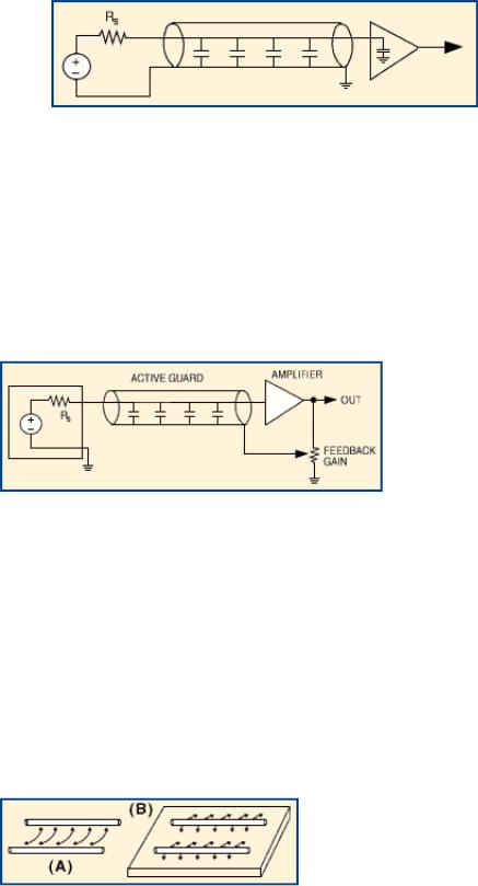
Other than the obvious strategies for reducing parasitic capacitance through shorter transducer-to-front end runs and the use of low-capacitance cables and low-input capacitance amplifiers (all good ideas), the best way to deal with this problem is to use an active guard (see Figure 11). An active guard feeds a replica of the input signal to a shield surrounding the signal conductor, as opposed to connecting the shield to ground. Because the voltage in the guard follows the signal conductor voltage, the total change in their difference remains zero. Thus, there is effectively no capacitance between them.
Figure 11. An active guard is an elegant solution to the problem of cable capacitance. By driving the shield with a replica of the input signal, you don't charge or discharge the cable capacitance, which makes it appear to be zero. Depending on the properties of the sensor and amplifier, however, you may have to adjust the amount of signal you feed back to maintain stability.
One problem that you frequently encounter when using a dynamic guard is that of stability. Depending on the characteristics of the transducer and the front-end amplifier, you may have to reduce the feedback gain to less than one to prevent the system from oscillating. The potentiometer shown in Figure 10 provides such a gain-control function.
Capacitive pickup occurs when a nearby time-varying signal line couples into the signal line of interest (see Figure 12). High-impedance signal
Figure 12. Electrostatic coupling occurs when electric fields pass from one conductor to another (A). While providing continuous shields around the conductors can greatly reduce the problem, in many cases the use of a nearby groundplane (B) will also suffice. The groundplane swallows stray fields emanating from the conductors. This is easy to implement on PCBs.
lines are especially susceptible to this problem because the coupling capacitance—which may be only in the picofarad range—can have lower impedance at frequencies of interest than the transducer. As the frequency of
http://www.sensorsmag.com/articles/0598/sig0598/main.shtml |
Página 9 de 10 |

Sensors - May 1998 - Interfacing Sensors |
and Signal Processing Components |
21/08/2002 09:00 |
the interfering signal increases, the coupling capacitance's impedance drops.
To fix this type of problem, you can either move the offending source away or shield the sensitive circuit. While the term shielding often invokes visions of coaxial cable and die-cast metal boxes (sometimes the only effective options), it can also take less costly forms. The ground plane shown in Figure 12 is one such method. By "swallowing" lines of electric field emanating from the signal source, the technique reduces the mutual coupling between the conductors. Ground planes are easily fabricated on PCBs and flex circuits, making them one of the most easily manufactured shielding approaches.
Shielded cable is also useful for reducing capacitively coupled interference (in addition to RF interference in general) because offending fields are stopped at the shield. Remember, however, that for maximum effectiveness, a shield must be grounded. Grounding it at one end (usually the one closest to the front-end amplifier) is usually the best method. Grounding the shield at both ends can cause problems resulting from currents running along the shield. There are several styles of shield: foil with drain wire, spiral wrapped, and braided. Although cable that has a braided shield looks more impressive than cable with a foil shield and drain wire, both are effective at moderate frequencies.
Ed Ramsden is Senior Engineer, Sensor Devices, Cherry Electrical Products, 40 Terrill Park Dr., Concord, NH 03301; 603-224-4513, fax 603-224-5843.
We Love Feedback
Sensors® and Sensors Expo® are registered trademarks of Advanstar Communications Inc.
Sensors Online Home | Sensors Expo | Contact Us
http://www.sensorsmag.com/articles/0598/sig0598/main.shtml |
Página 10 de 10 |