

6.12. Дублирование регистра.
Задержка в цепи распространения сигнала возрастает с увеличением числа входов, нагруженных на эту цепь. Такая ситуация еще может быть приемлема для цепей сброса, но для цепей разрешения это недопустимо. Пример такой ситуации приведен ниже (Рис.6.29). В данном VHDL примере коэффициент разветвления сигнала разрешения "Tri_en" равен 24.
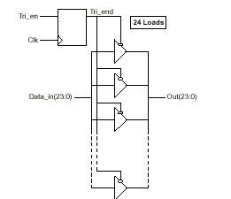
Рис.6.29.
architecture load of four_load is
signal Tri_en std_logic;
begin
loadpro: process (Clk)
begin
if (clk'event and clk ='1') then
Tri_end <= Tri_en;
end if;
end process loadpro;
endpro : process (Tri_end, Data_in)
begin
if (Tri_end = '1') then
out <= Data_in;
else
out <= (others => 'Z');
end if;
end process endpro;
end load;
Число разветвлений (fanout) можно уменьшить вдвое, используя два регистра (Рис.6.30)
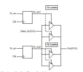
Рис.6.30
Ниже приведен пример реализации дублирования регистров на VHDL.
architecture loada of two_load is
signal Tri_en1, Tri_en2 : std_logic;
begin
loadpro: process (Clk)
begin
if (clk'event and clk ='1') then
Tri_en1 <= Tri_en;
Tri_en2 <= Tri_en;
end if;
end process loadpro;
process (Tri_en1, Data_in)
begin
if (Tri_en1 = '1') then
out(23:12) <= Data_in(23:12);
else
out(23:12) <= (others => 'Z');
end if;
end process;
process (Tri_en2, Data_in)
begin
if (Tri_en2 = '1') then
out(11:0) <= Data_in(11:0);
else
out(11:0) <= (others => 'Z');
end if;
end process;
Разделение проекта на части оптимальных размеров позволяет обеспечить оптимальное использование ресурсов за счет их оптимизации при синтезе. Известно, что подавляющее большинство программ синтеза достигают наиболее приемлимого результата при размере блока порядка 2-5 тысяч эквивалентных вентилей.
Приведенный ниже пример показывает как можно сэкономить ресурсы путем замены встроенного в модуль регистра(Рис.6.31) на выделенный регистр (рис 3.32)
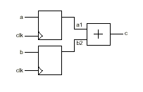
Рис.6.31
process (clk, a, b) begin
if (clk'event and clk = '1') then
a1 <= a;
b1 <=b;
end if;
end process;
process (a1, b1)
begin c <=a1 +b1;
end process;
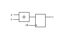
Рис.6.32
process (clk, a, b) begin
if (clk'event and clk = '1') then
c <=a +b;
end if;
end process;
6.13.Создание описаний с учетом особенностей архитектуры плис (Technology Specific Coding Techniques).
Помимо способов создания описаний, независимых от используемой элементной базы и ее архитектурных особенностей, в практике проектирования устройств на ПЛИС применяется так называемое создание описаний с учетом особенностей архитектуры ПЛИС (Technology Specific Coding Techniques).
Рассмотрим некоторые примеры проектирования цифровых устройств для использования с учетом особенностей архитектуры FPGA ПЛИС.
Для реализации мультиплексоров как правило применяется конструкция case, что значительно выгоднее с точки зрения быстродействия и затрат ресурсов, чем конструкция if-then-else. Большинство производителей ПЛИС рекоммендуют использовать оператор case.
Как правило, при реализации на ПЛИС внутренняя шина с тремя состояниями эмулируется как мультиплексор. Пример эмуляции шины в виде мультиплексора приведен на Рис.6.33
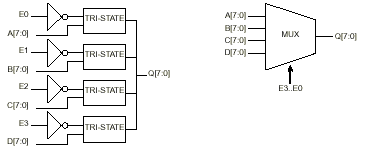
Рис.6.33
Пример эмуляции шины на VHDL
library IEEE;
use IEEE.std_logic_1164.all;
entity tribus is
port (A, B, C, D : in std_logic_vector(7 downto 0);
E0, E1, E2, E3 : in std_logic;
Q :out std_logic_vector(7 downto 0));
end tribus;
architecture rtl of tribus is
begin
Q <=Awhen(E0 = '1') else "ZZZZZZZZ";
Q <=Bwhen(E1 = '1') else "ZZZZZZZZ";
Q <=Cwhen(E2 = '1') else "ZZZZZZZZ";
Q <=Dwhen(E3 = '1') else "ZZZZZZZZ";
end rtl;
Мультиплексор на VHDL
library IEEE;
use IEEE.std_logic_1164.all;
entity muxbus is
port (A, B, C, D : in std_logic_vector(7 downto 0);
E0, E1, E2, E3 : in std_logic;
Q :out std_logic_vector(7 downto 0));
end muxbus;
architecture rtl of muxbus is
signal E_int : std_logic_vector(1 downto 0);
begin
process (E0, E1, E2, E3)
variable E : std_logic_vector(3 downto 0);
begin
E :=E0 &E1 &E2 &E3;
case E is
when "0001" => E_int <= "00";
when "0010" => E_int <= "01";
when "0100" => E_int <= "10";
when "1000" => E_int <= "11";
when others => E_int <= "--";
end case;
end process;
process (E_int, A, B, C, D)
begin
case E_int is
when "00" => Q <= D;
when "01" => Q <= C;
when "10" => Q <= B;
when "11" => Q <= A;
when others =>Q <=(others => '-');
end case;
end process;
end rtl;
Эмуляция шины на Verilog
module tribus (A, B, C, D, E0, E1, E2, E3, Q);
input [7:0]A, B, C, D;
output [7:0]Q;
input E0, E1, E2, E3;
assign Q[7:0] = E0 ? A[7:0] : 8'bzzzzzzzz;
assign Q[7:0] = E1 ? B[7:0] : 8'bzzzzzzzz;
assign Q[7:0] = E2 ? C[7:0] : 8'bzzzzzzzz;
assign Q[7:0] = E3 ? D[7:0] : 8'bzzzzzzzz;
endmodule
Реализация мультиплексора на Verilog
module muxbus (A, B, C, D, E0, E1, E2, E3, Q);
input [7:0]A, B, C, D;
output [7:0]Q;
input E0, E1, E2, E3;
wire [3:0] select4;
reg [1:0] select2;
reg [7:0]Q;
assign select4 = {E0, E1, E2, E3};
always @ (select4)
begin
case(select4)
4'b0001 : select2 = 2'b00;
4'b0010 : select2 = 2'b01;
4'b0100 : select2 = 2'b10;
4'b1000 : select2 = 2'b11;
default : select2 = 2'bxx;
endcase
end
always @ (select2 or A or B or C or D)
begin
case(select2)
2'b00 :Q =D;
2'b01 :Q =C;
2'b10 :Q =B;
2'b11 :Q =A;
endcase
end
endmodule
Несколько примеров хотелось бы привести по реализации устройств памяти
Приведенный ниже пример иллюстрирует описание статической памяти (SRAM) на VHDL для реализации на ПЛИС, не имеющих встроенных блоков памяти. В ряде случаев этот прием позволяет не выходя за рамки одного устройствареализовать небольшой буфер. Пример реализован на VHDL
-- *************************************************
-- Behavioral description of a single-port SRAM with:
-- Active High write enable (WE)
-- Rising clock edge (Clock)
-- *************************************************
library ieee;
use ieee.std_logic_1164.all;
use IEEE.std_logic_arith.all;
use IEEE.std_logic_unsigned.all;
entity reg_sram is
generic (width : integer:=8;
depth : integer:=8;
addr : integer:=3);
port (Data : in std_logic_vector (width-1 downto 0);
Q :out std_logic_vector (width-1 downto 0);
Clock : in std_logic;
WE : in std_logic;
Address : in std_logic_vector (addr-1 downto 0));
end reg_sram;
architecture behav of reg_sram is
type MEM is array (0 to depth-1) of std_logic_vector(width-1
downto 0);
signal ramTmp : MEM;
begin
process (Clock)
begin
if (clock'event and clock='1') then
if (WE = '1') then
ramTmp (conv_integer (Address)) <= Data;
end if;
end if;
end process;
Q <= ramTmp(conv_integer(Address));
end behav;
Модель на Verilog имеет вид
`timescale 1 ns/100 ps
//########################################################
//# Behavioral single-port SRAM description :
//# Active High write enable (WE)
//# Rising clock edge (Clock)
//#######################################################
module reg_sram (Data, Q, Clock, WE, Address);
parameter width = 8;
parameter depth = 8;
parameter addr = 3;
input Clock, WE;
input [addr-1:0] Address;
input [width-1:0] Data;
output [width-1:0] Q;
wire [width-1:0] Q;
reg [width-1:0] mem_data [depth-1:0];
always @(posedge Clock)
if(WE)
mem_data[Address] = #1 Data;
assign Q = mem_data[Address];
endmodule
Следующий пример иллюстрирует создание модели двупортовой статической памяти (Dual-Port SRAM). Описывается модуль 8 х 8 ячеек.
Описание на VHDL имеет вид
-- Behavioral description of dual-port SRAM with :
-- Active High write enable (WE)
-- Active High read enable (RE)
-- Rising clock edge (Clock)
library ieee;
use ieee.std_logic_1164.all;
use IEEE.std_logic_arith.all;
use IEEE.std_logic_unsigned.all;
entity reg_dpram is
generic (width : integer:=8;
depth : integer:=8;
addr : integer:=3);
port (Data : in std_logic_vector (width-1 downto 0);
Q :out std_logic_vector (width-1 downto 0);
Clock : in std_logic;
WE : in std_logic;
RE : in std_logic;
WAddress: in std_logic_vector (addr-1 downto 0);
RAddress: in std_logic_vector (addr-1 downto 0));
end reg_dpram;
architecture behav of reg_dpram is
type MEM is array (0 to depth-1) of std_logic_vector(width-1
downto 0);
signal ramTmp : MEM;
begin
-- Write Functional Section
process (Clock)
begin
if (clock'event and clock='1') then
if (WE = '1') then
ramTmp (conv_integer (WAddress)) <= Data;
end if;
end if;
end process;
-- Read Functional Section
process (Clock)
begin
if (clock'event and clock='1') then
if (RE = '1') then
Q <= ramTmp(conv_integer (RAddress));
end if;
end if;
end process;
end behav;
Модель двупортовой памяти на Verilog
`timescale 1 ns/100 ps
//########################################################
//# Behavioral dual-port SRAM description :
//# Active High write enable (WE)
//# Active High read enable (RE)
//# Rising clock edge (Clock)
//#######################################################
module reg_dpram (Data, Q, Clock, WE, RE, WAddress, RAddress);
parameter width = 8;
parameter depth = 8;
parameter addr = 3;
input Clock, WE, RE;
input [addr-1:0] WAddress, RAddress;
input [width-1:0] Data;
output [width-1:0] Q;
reg [width-1:0] Q;
reg [width-1:0] mem_data [depth-1:0];
// ######################################################
// # Write Functional Section
// ######################################################
always @(posedge Clock)
begin
if(WE)
mem_data[WAddress] = #1 Data;
end
//####################################################
//# Read Functional Section
//####################################################
always @(posedge Clock)
begin
if(RE)
Q = #1 mem_data[RAddress];
end
endmodule