

Laboratory work № 6- 9 studying of light-emitting diode
1 Goal of the work:
Studying of transformation of an electrical energy into the light by light-emitting diode and measuring of its electric and light characteristics.
2 Main concepts
2.1 P-N junction
P-n junction usually appears in internal part of a crystal conductor where type of dopant changes from acceptor to donor and, related with this, type of conductivity, from hole to electron.
If there is no contact between semiconductors of p- and n- types then theirs Fermi levels are situated on a different heights: in p- type - closer to the valence band, and in n-type - close to the conductivity band (work function of electron from the p-region always
|
|
|
a) |
b) |
c) |
Figure 25 – p-n junction at zero (a), forward (b) and reverse (c) bias |
||


is greater than the work function from the n-region).
When the contact appears (Fig. 25a) exchange of charge takes place in a result of which Fermi level becomes align. In the near-contact area appears depletion region which is depleted by the majority carriers: by electrons – from the side of the electron semiconductor, by holes – from the side of the holes semiconductor. Ions of impurities of this level create positive volume charge in the n-region and negative - in the p-region. Between n- and p- regions establishes built-in potential difference ΔφBI which resists to the movement of majority carriers. That’s why, to pass the p-n region, majority carriers must overcome the potential barrier e· ΔφBI.
If we short-circuit some of the ends of two regions of the p-n junction then there will be no current in the circuit. It means that at the equilibrium, total current, created by the movement of majority and minority carriers through the contact junction, will be equal to zero.
Connection of the external voltage of the direct polarity (forward bias) to the contact (plus – to p-semiconductor, minus – to n-semiconductor) leads to decreasing of the potential barrier (Fig. 25b). Number of majority carriers, which are able to penetrate through the p-n junction increases, flux of minority carries stays the same. Current flows in the forward direction through the junction.
If we apply to the junction reverse bias (Fig. 25c) then the external field of the reverse polarity sums with the internal field of the depletion region. Meanwhile for the diffusion current of the majority carriers appears great resistance. Through the contact flows the current of the reverse direction, which is in many times less than the forward direction current. Transition of minority carriers will have been finished at some value of reverse bias voltage. The reverse current, created only by the minority carriers, gets its saturation.
2.2 Led properties
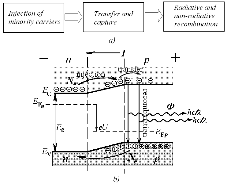
In optical communication devices as a light source are used light-emitting diodes (LED), working in a mode of spontaneous emission (light-emitting diode) or in a stimulated emission mode (laser). Let’s consider the principle of work of such diode.
Phenomenon of light emission during the flow of current is called the electroluminescence, and during the direct current flow through the p-n junction - injection electroluminescence.
 Figure
23
–
Electrolumiscence in р-n-junction.
Figure
23
–
Electrolumiscence in р-n-junction.
Figure
24
–
CVC of LED.
C urrent-Voltage
characteristic
(CVC) of LED ILED=f(U)
has the appearance which is typical for a diode (Fig
24)
and can be characterized by a cutoff
voltage
UCUT
and residual
resistance RRES.
Cutoff voltage is received by an extrapolation of a linear section of
a CVC to the current zero. Its value is close to the value of p-n
junction built-in potential. Residual resistance RRES
is determined as a cotangent of the slope angle of the linear section
of a CVC.
urrent-Voltage
characteristic
(CVC) of LED ILED=f(U)
has the appearance which is typical for a diode (Fig
24)
and can be characterized by a cutoff
voltage
UCUT
and residual
resistance RRES.
Cutoff voltage is received by an extrapolation of a linear section of
a CVC to the current zero. Its value is close to the value of p-n
junction built-in potential. Residual resistance RRES
is determined as a cotangent of the slope angle of the linear section
of a CVC.
Light characteristic of LED Ф=f(I) is the dependence of a power of emission Ф on the current I. Usually this characteristic is sublinear for small currents and linear for big ones. On small currents channels of non-radiative recombination play a big role and on big currents some of these channels become saturated and it leads to increasing of LED effectiveness.
3 Description of laboratory research facility and methodology of measurements Scheme of the research facility for measuring of LED parameters is shown on the Fig. 24. Here B – supply battery of a scheme, mА – milliamperemeter for measuring of current through LED, V – voltmeter for measuring of voltage through the LED, LED – studied light-emitting diode, PD – photodiode for measuring of emission power of the LED, А – microamperemeter for measuring of current through the PD.
Light – emitting diode and the photodiode are located in a lightproof tube as close as it’s possible. The LED forward bias current is gradually varying by the resistance box R. Light emission, caused by this current, is detected by photodiode with known sensitivity S. This photocurrent is measured by microamperemeter. Limiting value of the LED current is about 50 mA and is limited by internal resistance of a battery.
 Figure
24
-
Scheme
of the research
facility
Figure
24
-
Scheme
of the research
facility
Efficiency of transformation of the electric energy into light one can be characterized by the energy efficiency:
![]() ,
,
where PLIGHT - emitted light power, PE - electric power consumption, IPD - current through the photodiode, SPD - photodiode sensitivity in μA/mW, I LED- current through the LED, U – voltage on the LED;
and by the quantum efficiency:
![]() ,
,
where NPH - number of emitted photons, NCH - number of charge carriers which have passed the p-n junction, e - charge of electron, λ - wavelength of light, h=6.63·10-34J·s - Planck constant, c = 3·108 m/s - speed of light.
Energy and quantum efficiency have close values because photon energy values is close to the forbidden energy gap width and applied voltage value is close to the forbidden energy gap width divided by the charge of electron.