


Operation
Standalone Application Example
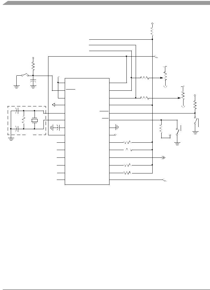
Figure 12 shows an application example of the MC3PHAC, configured in standalone mode. Resistor values and jumpers have been selected to provide the following performance:
1.Base frequency of 60 Hz and positive PWM polarity (from Table 3)
2.PWM frequency resistor 3.9 kΩ, which implies 10.582 kHz from Table 4). (5v/(3.9k + 6.8k))*3.9k = 1.82 volts
3.Dead-time resistor = 5.1 kΩ, which implies 4.5 µs (from Figure 9)
4.Fault retry time resistor = 8.2 kΩ, which implies 32.8 seconds (from Figure 10).
5.Voltage boost resistor = 12 kΩ, which implies 25.5 percent (from Figure 11).
6.The wiper of the acceleration potentiometer is set at 2.5 V = 64 Hz/second acceleration rate (from the Acceleration Control description on page 11.) The potentiometer, in this case, could have been
a resistor divider. If a resistor divider is used in place of the acceleration potentiometer, keep the total resistance of the two resistors less than 10 kΩ. Always use 4.7kΩ in series with the center of the acceleration voltage divider resistors, connected to the ACCEL (pin 27) as shown in the application example, Figure 12.
7.Crystal/resonator capacitor values are typical values from the manufacturer. Refer to the manufacturers data for actual values.
PC Master Software Operation
Introduction to PC Master Host Software
The MC3PHAC is compatible with Freescale’s PC master host software serial interface protocol. Communication occurs over an on-chip UART, on the MC3PHAC at 9600 baud to an external master device, which may be a microcontroller that also has an integrated UART or a personal computer via a COM port. With PC master software, an external controller can monitor and control all aspects of the MC3PHAC operation.
When the MC3PHAC is placed in PC master software mode, all control of the system is provided through the integrated UART, resident on the MC3PHAC. Inputs such as START, FWD, SPEED, ACCEL, MUX_IN, and PWMPOL_BASEFREQ have no controlling influence over operation of the system. Even though the SPEED, START, and FWD inputs are disabled while the system is in PC master software mode, through PC master software, it is possible to monitor the state of those inputs.
The most popular master implementation is a PC, where a graphical user interface (GUI) has been layered on top of the PC master software command protocol, complete with a graphical data display, and an ActiveX interface. Figure 13 shows the MC3PHAC configured in PC master software mode. It is
beyond the scope of this document to describe the PC master software protocol or its implementation on a personal computer. For further information on these topics, refer to other Freescale documents relating
to the PC master software protocol and availability of PC master host software.
MC3PHAC Monolithic Intelligent Motor Controller, Rev. 2
Freescale Semiconductor |
19 |
Operation
|
|
|
|
|
|
|
|
|
|
|
|
+5 V |
|
|
|
|
|
|
|
|
|
|
|
|
|
|
|
|
|
|
6.8 kΩ |
|
|
|
|
|
|
|
|
|
|
|
|
NC |
|
50 Hz – PWM POLARITY |
|
|
|
|
|
|
|
|
||
|
|
|
|
|
|
|
50 Hz + PWM POLARITY |
|
|
|
|
|
|
|
|
|||
|
|
|
|
|
|
NC |
|
|
|
|
|
|
|
|
|
|||
|
|
|
|
|
|
|
|
|
|
|
|
|
|
|
|
|
|
|
|
|
|
|
|
|
NC |
|
60 Hz – PWM POLARITY |
|
|
|
|
|
|
|
|
||
|
|
|
|
|
|
|
|
|
|
|
|
|
|
|
|
|
|
|
|
+5 V |
|
|
|
|
|
60 Hz + PWM POLARITY |
|
FROM DIVIDED DC BUS |
|
||||||||
|
|
|
|
|
|
|
|
|
|
|
|
|
||||||
|
|
10 kΩ |
|
|
|
|
|
|
|
|
|
+5 A |
POT |
|
|
|
||
|
|
|
|
|
|
|
|
|
|
|
|
|
|
|
|
|||
|
|
|
|
|
|
|
|
|
|
|
|
|
|
|
|
|
||
|
|
|
|
NOTE 6 |
RESET |
|
ACCEL |
27 |
|
4.7 kΩ |
5 kΩ |
|
ACCELERATION |
|
POT |
|
||
|
|
|
|
|
2 |
|
|
|
|
|
|
|
||||||
|
|
|
|
|
+5 A |
MC3PHAC |
|
|
|
|
|
|
|
|
|
|
||
RESET |
0.1 |
µF |
|
1 |
VREF |
|
DC_BUS |
28 |
|
|
|
A |
|
|
|
|
|
|
|
|
|
|
|
|
|
|
|
+5 A |
|
|
|||||||
|
|
|
|
|
|
|
|
|
|
|
|
|
|
|
|
|
||
|
|
|
|
|
3 |
|
|
|
26 |
|
4.7 kΩ |
|
|
|
|
5 kΩ |
SPEED |
+5 V |
|
|
|
|
|
|
|
SPEED |
|
|
|
|
|
|
|
||||
|
|
|
|
|
VDDA |
|
|
|
|
|
|
|
|
|
||||
|
|
|
|
|
|
|
|
|
|
|
|
|
|
|
||||
|
|
|
|
|
4 |
VSSA |
|
MUX_IN |
25 |
|
|
|
|
|
|
A |
|
10 kΩ |
|
|
4.0MHz |
|
|
A |
|
|
VDD |
|
|
|
|
|
|
|
FOR/REV |
|
START/STOP |
|
|
|
|
8 |
PWMPOL_BASEFREQ |
21 |
+ 5 |
|
|
|
|
|
|
|||||
22 pF |
10 MΩ |
|
|
|
5 |
OSC2 |
|
START |
24 |
|
|
|
|
|
|
|
|
|
|
|
|
|
|
6 |
OSC1 |
|
FWD |
23 |
|
|
|
|
|
|
|
|
|
22 pF |
|
|
|
0.1 µF |
|
|
|
|
|
|
|
|
|
|
|
|
|
|
|
|
|
|
7 |
PLLCAP |
|
VSS |
22 |
|
|
|
|
|
|
|
|
|
|
|
|
|
|
|
|
NOTE 6 |
|
|
10 kΩ |
|
|
|
||||||
|
NOTE 7 |
|
|
|
|
|
|
|
|
|
|
|
|
+ 5 |
|
|
|
|
|
|
|
|
|
|
|
|
|
|
|
|
|
|
|
|
|
||
|
|
|
|
|
9 |
PWM_U_TOP |
VBOOST_MODE |
20 |
12 kΩRBOOST |
NOTE 1 |
|
|
|
|
|
|
|
|
|
|
|
|
|
10 |
PWM_U_BOT |
DT_FAULTOUT |
19 |
RDEADTIME |
NOTE 2 |
|
|
|
|
|
|
|
|
|
|
|
|
POWERSTAGE |
|
|
5.1 kΩ |
|
|
|
|
|
|
|
|
|||
|
|
|
PWMs—6 TO |
13 |
|
|
|
16 |
NOTE 4 |
|
|
|
|
|
|
|
||
|
|
|
PWM_V_TOP |
|
RBRAKE |
RPWMFREQ |
|
|
TO RESISTIVE BRAKE DRIVER |
|||||||||
|
|
|
|
|
11 |
|
18 |
RRETRY |
|
|
|
|||||||
|
|
|
|
|
12 |
PWM_V_BOT |
RETRY/TxD |
17 8.2 kΩ |
NOTE 3 |
|
|
|
|
|
|
|
||
|
|
|
|
|
|
|
|
|
|
|
|
|
||||||
|
|
|
|
|
|
PWM_W_TOP |
PWMFREQ/RxD |
|
3.9 kΩ |
|
|
|
|
|
|
|
|
|
|
|
|
|
|
14 |
PWM_W_BOT |
|
FAULTIN |
15 |
|
NOTE 5 |
|
FROM SYSTEM FAULT |
|||||
|
|
|
|
|
|
|
|
|
||||||||||
|
|
|
|
|
|
|
|
|
|
|
|
DETECTION CIRCUIT |
||||||
|
|
|
|
|
|
|
|
|
|
|
|
|
|
|||||
Notes:
1.See Figure 11.
2.See Figure 9.
3.See Figure 10.
4.See Table 4.
5.If no external fault circuit is provided, connect to VSS.
6.Use bypass capacitors placed close to the MC3PHAC.
7.Consult crystal/resonator manufacturer for component values.
Figure 12. MC3PHAC Application Example in Standalone Mode
MC3PHAC Monolithic Intelligent Motor Controller, Rev. 2
20 |
Freescale Semiconductor |
|
+5 V |
|
|
|
|
|
10 kΩ |
NOTE 2 |
|
|
|
|
|
+5 A |
|
|
|
|
1 |
RESET |
0.1 µF |
|
2 |
|
|
|
|
|
|
|
|
|
|
3 |
|
|
|
|
4 |
22 pF |
10 MΩ |
4.0 MHz |
|
A |
|
5 |
|||
|
|
|||
22 pF |
|
|
6 |
|
|
|
|
0.1 µF |
|
|
NOTE 3 |
|
|
7 |
|
+5 V |
|
|
8 |
|
10 kΩ |
|
|
|
|
|
|
9 |
|
|
|
|
|
|
|
|
|
|
10 |
|
|
6 — PWMs TO |
POWER STAGE |
11 |
|
|
12 |
||
|
|
13 |
||
|
|
|
||
|
|
|
|
14 |
|
|
|
|
|
|
Operation |
|
MC3PHAC |
|
|
|
|
|
||
VREF |
|
DC_BUS 28 |
|
FROM DIVIDED DC BUS |
|||
RESET |
|
ACCEL 27 |
10 kΩ |
|
|
||
VDDA |
|
SPEED 26 |
+5 V |
|
|||
|
|
|
|||||
VSSA |
|
MUX_IN 25 |
|
|
|
||
OSC2 |
|
START |
24 |
|
560 Ω |
|
|
OSC1 |
|
FWD 23 |
|
|
|
||
PLLCAP |
|
VSS |
22 |
|
|
|
|
|
|
NOTE 2 |
FAULT LED |
|
|||
|
|
VDD |
21 |
|
|||
PWMPOL_BASEFREQ |
+ 5 |
|
|
||||
|
|
|
|||||
PWM_U_TOP |
VBOOST_MODE 20 |
|
|
|
|||
PWM_U_BOT |
DT_FAULTOUT |
19 |
|
|
|
||
PWM_V_TOP |
|
RBRAKE 18 |
|
TO RESISTIVE BRAKE DRIVER |
|||
PWM_V_BOT |
RETRY/TxD 17 |
DATA TO PC |
ISOLATED |
CONNECTION |
|||
|
|
|
|
|
OR NON-ISOLATED |
||
|
PWMFREQ/RxD 16 |
DATA FROM PC |
TO HOST |
||||
PWM_W_TOP |
RS232 INTERFACE |
||||||
|
|
||||||
PWM_W_BOT |
|
FAULTIN |
15 |
NOTE 1 |
FROM SYSTEM FAULT |
||
|
|
|
DETECTION CIRCUIT |
||||
|
|
|
|
|
|||
Notes:
1.If no external fault circuit is provided, connect to VSS.
2.Use bypass capacitors placed close to the MC3PHAC.
3.Consult crystal/resonator manufacturer for component values.
Figure 13. MC3PHAC Configuration for Using a PC as a Master
PC Master Software Operation with the MC3PHAC
When power is first applied to the MC3PHAC, or if a logic low level is applied to the RESET pin, the MC3PHAC enters PC master software mode if the VBOOST_MODE pin is low during the initialization phase. The MC3PHAC recognizes a subset of the PC master software command set, which is listed in Table 5.
Table 5. Recognized PC Host Software Commands
Command |
Description |
|
|
|
|
GETINFOBRIEF |
MC3PHAC responds with brief summary of hardware setup and link configuration |
|
information |
||
|
||
|
|
|
READVAR8 |
MC3PHAC reads an 8-bit variable at a specified address and responds with its value |
|
|
|
|
READVAR16 |
MC3PHAC reads a 16-bit variable at a specified address and responds with its value |
|
|
|
|
READVAR32 |
MC3PHAC reads a 32-bit variable at a specified address and responds with its value |
|
|
|
|
WRITEVAR8 |
MC3PHAC writes an 8-bit variable at a specified address |
|
|
|
|
WRITEVAR16 |
MC3PHAC writes a 16-bit variable at a specified address |
|
|
|
With the READVARx commands, the addresses are checked for validity, and the command is executed only if the address is within proper limits. In general, a read command with an address value below $0060 or above $EE03 will not execute properly, but instead will return an invalid operation response. An
MC3PHAC Monolithic Intelligent Motor Controller, Rev. 2
Freescale Semiconductor |
21 |

Operation
exception to this rule is that PC master software allows reading locations $0001, $0036 and $FE01, which are PORTB data register, Dead Time register and SIM Reset Status registers respectively. The addresses for the WRITEVARx commands are checked for validity, and the data field is also limited to a valid range for each variable. See Table 6 for a list of valid data values and valid write addresses.
User interface variables and their associated PC master software addresses within the MC3PHAC are listed in Table 6.
Table 6. User Interface Variables for Use with PC Master Software
Name |
Address |
Read/ |
Size |
Description |
Valid Data |
|
Write |
(Bytes) |
|||||
|
|
|
|
|||
|
|
|
|
|
|
|
|
|
|
|
Determines whether the motor should |
Forward — $10 |
|
Commanded direction |
$1000 |
W |
1 |
Reverse — $11 |
||
go forward, reverse, or stop |
||||||
|
|
|
|
Stop — $20 |
||
|
|
|
|
|
||
|
|
|
|
|
|
|
Command reset |
$1000 |
W |
1 |
Forces the MC3PHAC to perform an |
$30 |
|
immediate reset |
||||||
|
|
|
|
|
||
|
|
|
|
|
|
|
|
|
|
|
|
5.3 kHz — $41 |
|
Commanded PWM |
$1000 |
W |
1 |
Specifies the frequency of the |
10.6 kHz — $42 |
|
frequency(1) |
MC3PHAC PWM frequency |
15.9 kHz — $44 |
||||
|
|
|
||||
|
|
|
|
|
21.1 kHz — $48 |
|
|
|
|
|
|
|
|
|
|
|
|
The modulus value supplied to the |
|
|
Measured PWM |
$00A8 |
R |
2 |
PWM generator used by the |
$00BD–$05E8 |
|
period |
MC3PHAC — value is multiplied by |
|||||
|
|
|
|
|||
|
|
|
|
250 ns to obtain PWM period |
|
|
|
|
|
|
|
|
|
|
|
|
|
Specifies the polarity of the MC3PHAC |
B + T + $50 |
|
|
|
|
|
PWM outputs. This is a write once |
||
Commanded PWM |
|
|
|
B + T – $54 |
||
$1000 |
W |
1 |
parameter after reset. |
|||
polarity(2), (3), (4) |
B – T + $58 |
|||||
|
|
|
Example: $50 = Bottom and top PWM |
|||
|
|
|
|
B – T – $5C |
||
|
|
|
|
outputs are positive polarity. |
||
|
|
|
|
|
||
|
|
|
|
|
|
|
|
|
|
|
Specifies the dead time used by the |
|
|
Dead time(2), (3), (4) |
$0036 |
R/W |
1 |
PWM generator. |
$00–$FF |
|
Dead time = Value * 125 ns. |
||||||
|
|
|
|
|
||
|
|
|
|
This is a write-once parameter. |
|
|
|
|
|
|
|
|
|
Base frequency(3) |
$1000 |
W |
1 |
Specifies the motor frequency at which |
60 Hz — $60 |
|
full voltage is applied |
50 Hz — $61 |
|||||
|
|
|
|
|||
|
|
|
|
|
|
|
Acceleration(3) |
$0060 |
R/W |
2 |
Acceleration in Hz/sec (7.9 format)(8) |
$0000–$7FFF |
|
Commanded motor |
$0062 |
R/W |
2 |
Commanded frequency in Hz. |
$0000–$7FFF |
|
frequency(3) |
(8.8 format)(9) |
|||||
|
|
|
|
|||
Actual frequency |
$0085 |
R |
2 |
Actual frequency in Hz. (8.8 format)(9) |
$0000–$7FFF |
|
Status(7) |
$00C8 |
R |
1 |
Status byte |
$00–$FF |
|
Voltage boost |
$006C |
R/W |
1 |
0 Hz voltage. |
$00–$FF |
|
%Voltage boost = Value/$FF |
||||||
|
|
|
|
|
||
|
|
|
|
|
|
|
|
|
|
|
Voltage level (motor waveform |
|
|
Modulation index |
$0091 |
R |
1 |
amplitude percent assuming no bus |
$00–$FF |
|
ripple compensation) |
||||||
|
|
|
|
|
||
|
|
|
|
Modulation index = value/$FF |
|
|
|
|
|
|
|
|
|
|
MC3PHAC Monolithic Intelligent Motor Controller, Rev. 2 |
|
||||
|
|
|
|
|
|
|
22 |
|
|
|
Freescale Semiconductor |
||

|
|
|
|
|
|
|
|
|
|
|
|
|
|
|
|
Operation |
|
|
|
Table 6. User Interface Variables for Use with PC Master Software (Continued) |
||||||
|
|
|
|
|
|
|
|
|
|
|
Name |
Address |
Read/ |
Size |
Description |
Valid Data |
|
|
|
Write |
(Bytes) |
|||||
|
|
|
|
|
|
|||
|
|
|
|
|
|
|
|
|
|
|
|
|
|
|
Maximum allowable modulation index |
|
|
Maximum voltage |
$0075 |
R/W |
1 |
value |
$00–$FF |
|||
|
|
|
|
|
|
%Maximum voltage = value/$FF |
|
|
|
|
|
|
|
|
|||
VBus voltage(5), (10) |
$0079 |
R |
2 |
DC bus voltage reading |
$000–$3FF |
|||
|
|
|
|
|
|
Specifies the delay time after a fault |
|
|
Fault timeout |
$006A |
R/W |
2 |
condition before re-enabling the |
$0000–$FFFF |
|||
motor. |
||||||||
|
|
|
|
|
|
|
||
|
|
|
|
|
|
Fault timeout = value * 0.262 sec |
|
|
|
|
|
|
|
|
|
|
|
Fault timer |
$006D |
R |
2 |
Real-time display of the fault timer |
$0000–$FFFF |
|||
Elapsed fault time = value * 0.262 sec |
||||||||
|
|
|
|
|
|
|
||
|
|
|
|
|
|
|
|
|
V |
Bus |
decel value(10) |
$00C9 |
R/W |
2 |
VBus readings above this value result in |
$0000–$03FF |
|
|
|
|
|
|
reduced deceleration. |
|
||
VBus RBRAKE |
$0064 |
R/W |
2 |
VBus readings above this value result in |
$0000–$03FF |
|||
|
value(10) |
|
|
|
the RBRAKE pin being asserted. |
|
||
VBus brownout |
$0066 |
R/W |
2 |
VBus readings below this value result in |
$0000–$03FF |
|||
|
value(10) |
|
|
|
an under voltage fault. |
|
||
VBus over voltage |
$0068 |
R/W |
2 |
VBus readings above this value result in |
$0000–$03FF |
|||
|
value(10) |
|
|
|
an over voltage fault. |
|
||
Speed in ADC |
$0095 |
R |
2 |
Left justified 10-bit ADC reading of the |
$0000–$FFC0 |
|||
|
value(5) |
SPEED input pin. |
||||||
|
|
|
|
|
||||
Setup(7) |
|
|
|
Bit field indicating which setup |
|
|||
$00AE |
R |
1 |
parameters have been initialized |
$E0–$FF |
||||
|
|
|
|
|
|
before motion is permitted |
|
|
|
|
|
|
|
|
|
|
|
Switch in(7) |
|
|
|
Bit field indicating the current state of |
|
|||
$0001 |
R |
1 |
the start/stop and forward/reverse |
$00–$FF |
||||
|
|
|
|
|
|
switches |
|
|
|
|
|
|
|
|
|||
Reset status(6), (7) |
$FE01 |
R |
1 |
Indicates cause of the last reset |
$00–$FF |
|||
Version |
$EE00 |
R |
4 |
MC3PHAC version |
ASCII field |
|||
|
|
|
|
|
|
|
|
|
1.The commanded PWM frequency cannot be written until the PWM outputs exit the high-impedance state. The default PWM frequency is 15.873 kHz.
2.The PWM output pins remain in a high-impedance state until this parameter is specified.
3.This parameter must be specified before motor motion can be initiated by the MC3PHAC.
4.This is a write-once parameter. The first write to this address will execute normally. Further attempts at writing this parameter will result in an illegal operation response from the MC3PHAC.
5.The value of this parameter is not valid until the PWM outputs exit the high-impedance state.
6.The data in this field is only valid for one read. Further reads will return a value of $00.
7.See register bit descriptions following this table.
8.Acceleration is an unsigned value with the upper seven bits range of $00 to $7F = acceleration value of 0 to
127 Hertz/second. The lower nine bits constitute the fractional portion of the acceleration parameter. Its range is $000 to $1FF which equals 0 to ~1. Therefore, the range of acceleration is 0 to 127.99 Hertz/second.
9.Commanded motor frequency and actual frequency are signed values with the upper byte range of
$00 to $7F = frequency of 0 to 127 Hz. The lower byte is the fractional portion of the frequency. Its range is $00 to $FF which equals 0 to ~1.
10.VBus is the voltage value applied to the DC_BUS analog input pin. The analog-to-digital converter is a 10-bit converter with a 5 volt full scale input. The value is equal to the voltage applied to the DC_BUS input pin/VREF * $03FF.
MC3PHAC Monolithic Intelligent Motor Controller, Rev. 2
Freescale Semiconductor |
23 |

Operation
Each bit variable listed in Table 6 is defined in Figure 14, Figure 15, Figure 16, and Figure 17.
Address: $00C8
|
|
|
7 |
|
|
6 |
5 |
4 |
|
3 |
|
2 |
1 |
|
0 |
|
R |
|
|
|
|
|
|
SPEED |
FORWARD |
MOTOR |
|
RESISTIVE |
|
EXTERNAL |
OVER |
|
UNDER |
|
|
|
|
|
|
|
|
|
VOLTAGE |
|
VOLTAGE |
|||||
|
|
|
|
|
|
|
CHANGING |
MOTION |
ENERGIZED |
|
BRAKE |
|
FAULT TRIP |
|
||
|
|
|
|
|
|
|
|
|
TRIP |
|
TRIP |
|||||
|
|
|
|
|
|
|
|
|
|
|
|
|
|
|
||
W |
|
|
|
|
|
|
|
|
|
|
|
|
|
|
|
|
|
|
|
|
|
|
|
|
|
|
|
|
|
|
|
||
|
|
|
|
|
|
|
|
|
|
|
|
|
|
|
|
|
Reset |
U |
|
0 |
1 |
0 |
|
0 |
|
U |
0 |
|
0 |
||||
|
|
|
|
|
|
|
= Unimplemented or Reserved |
|
U = Unaffected |
|
|
|
|
|||
|
|
|
|
|
|
|
|
|
|
|
|
|||||
|
|
|
|
|
|
|
|
Figure 14. Status Register |
|
|
|
|
||||
|
|
|
|
|
|
|
|
|
|
|
|
|||||
|
|
|
|
|
|
|
Table 7. Status Register Field Descriptions |
|
|
|
||||||
|
|
|
|
|
|
|
|
|
|
|
|
|||||
Field |
|
|
|
|
|
|
Description |
|
|
|
|
|||||
|
|
|
|
|
|
|||||||||||
6 |
|
|
|
|
SPEED CHANGING Bit — This read-only bit indicates if the motor is at a steady speed or if it is |
|||||||||||
SPEED |
|
|
accelerating or declerating. |
|
|
|
|
|
|
|
|
|||||
CHANGING |
|
|
0 |
Motor is at a steady speed. |
|
|
|
|
|
|
|
|
||||
|
|
|
|
|
1 |
Motor is accelerating or decelerating. |
|
|
|
|
|
|
|
|||
|
|
|
|
|
|
|||||||||||
5 |
|
|
|
|
FORWARD MOTION Bit — This read-only bit indicates the direction of the motor. It also indicates |
|||||||||||
FORWARD |
|
|
if the motor is stopped. |
|
|
|
|
|
|
|
|
|||||
MOTION |
|
|
0 |
Motor is rotating in the reverse direction. |
|
|
|
|
|
|
|
|||||
|
|
|
|
|
1 |
Motor is rotating in the forward direction. If this bit is a logic 1 and the actual frequency (location |
||||||||||
|
|
|
|
|
|
$0085 and $0086) is 0, the motor is stopped. |
|
|
|
|
||||||
|
|
|
|
|
|
|
||||||||||
4 |
|
|
|
|
MOTOR ENERGIZED Bit — This read-only bit indicates PWM output activity |
|
||||||||||
MOTOR |
|
|
0 |
The PWM outputs are inactive or the bottom PWM outputs are in the pre-charge cycle. |
||||||||||||
ENERGIZED |
|
|
1 |
All PWM outputs are active. |
|
|
|
|
|
|
|
|
||||
|
|
|
|
|
|
|||||||||||
3 |
|
|
|
|
RESISTIVE BREAK Bit — This read-only bit indicates the state of the RBRAKE output pin |
|||||||||||
RESISTIVE |
|
|
0 |
The RBRAKE output pin is inactive and no braking is in progress. |
|
|
|
|||||||||
BRAKE |
|
|
1 |
The RBRAKE output pin is active. Braking is in progress. |
|
|
|
|||||||||
|
|
|
|
|
|
|||||||||||
2 |
|
|
|
|
EXTERNAL FAULT TRIP Bit — This read-only bit indicates a FAULT has occurred resulting from |
|||||||||||
EXTERNAL |
|
|
a logic 1 applied to the FAULTIN pin. |
|
|
|
|
|
|
|
||||||
FAULT TRIP |
|
|
0 |
A logic 0 is applied to the FAULTIN pin and no FAULT timeout is in progress. |
|
|||||||||||
|
|
|
|
|
1 |
A logic 1 was applied to the FAULTIN pin and a FAULT timeout is still in progress. |
|
|||||||||
|
|
|
|
|
|
|||||||||||
1 |
|
|
|
|
OVER-VOLTAGE TRIP Bit — This read-only bit indicates if the voltage at the DC_BUS pin |
|||||||||||
OVER |
|
|
exceeds the preset value of VBus over voltage located at address $0068 and $0069. |
|
||||||||||||
VOLTAGE |
|
|
0 |
The voltage applied to the DC_BUS pin is less than the preset value of VBus over voltage and |
||||||||||||
TRIP |
|
|
|
a FAULT timeout is not in progress. |
|
|
|
|
|
|
|
|||||
|
|
|
|
|
1 |
The voltage applied to the DC_BUS pin has exceeded the preset value of VBus over voltage |
||||||||||
|
|
|
|
|
|
and a FAULT timeout is still in progress. |
|
|
|
|
|
|
|
|||
|
|
|
|
|
|
|||||||||||
0 |
|
|
|
|
UNDER-VOLTAGE Bit — This read-only bit indicates if the voltage at the DC_BUS pin is less |
|||||||||||
UNDER |
|
|
than the present value of VBus brownout located at address $0066 and $0067. |
|
||||||||||||
VOLTAGE |
|
|
0 |
The voltage applied to the DC-BUS pin is greater than the preset value of VBus under voltage |
||||||||||||
TRIP |
|
|
|
and a FAULT timeout is not in progress. |
|
|
|
|
|
|
|
|||||
|
|
|
|
|
1 |
The voltage applied to the DC_BUS pin is less than the present value of VBus under voltage |
||||||||||
|
|
|
|
|
|
and a FAULT timeout is still in progress. |
|
|
|
|
|
|
|
|||
|
|
|
|
|
|
|
|
|
|
|
||||||
|
|
|
|
|
|
|
MC3PHAC Monolithic Intelligent Motor Controller, Rev. 2 |
|
|
|
||||||
|
|
|
|
|
|
|
|
|
|
|
|
|
|
|
|
|
24 |
|
|
|
|
|
|
|
|
|
|
|
|
|
Freescale Semiconductor |
||

|
|
|
|
|
|
|
|
|
|
|
|
|
|
|
|
|
|
|
|
|
|
|
|
|
|
|
|
|
Operation |
Address: $00AE |
|
|
|
|
|
|
|
|
|
|
|
|||
|
|
|
7 |
|
6 |
5 |
4 |
|
3 |
2 |
1 |
|
0 |
|
|
|
|
|
|
|
|||||||||
R |
|
|
|
|
|
|
BASE |
|
SPEED |
ACCELERATION |
POLARITY |
|
DEAD TIME |
|
|
|
|
|
|
|
|
|
FREQUENCY |
|
|
||||
|
|
|
|
|
|
|
|
|
SET |
SET |
SET |
|
SET |
|
|
|
|
|
|
|
|
|
SET |
|
|
||||
|
|
|
|
|
|
|
|
|
|
|
|
|
|
|
W |
|
|
|
|
|
|
|
|
|
|
|
|
|
|
|
|
|
|
|
|
|
|
|
|
|
|
|
||
|
|
|
|
|
|
|
|
|
|
|
|
|
|
|
Reset |
1 |
|
1 |
1 |
0 |
|
0 |
0 |
0 |
|
0 |
|||
|
|
|
|
|
|
|
|
|
|
|
|
|
|
|
|
|
|
|
|
= Unimplemented or Reserved |
|
|
|
|
|
||||
|
|
|
|
|
|
|
Figure 15. Setup Register |
|
|
|
||||
|
|
|
|
|
|
|
|
|
|
|||||
|
|
|
|
|
|
Table 8. Setup Register Field Descriptions |
|
|
|
|||||
|
|
|
|
|
|
|
|
|
|
|
|
|
||
Field |
|
|
|
|
|
|
|
Description |
|
|
|
|
||
|
|
|
||||||||||||
4 |
|
BASE FREQUENCY SET Bit — This read-only bit indicates if the base frequency parameter has |
||||||||||||
BASE |
|
been set. |
|
|
|
|
|
|
|
|
|
|||
FREQUENCY |
0 |
Base frequency parameter has not been set. |
|
|
|
|
||||||||
SET |
|
1 |
Base frequency parameter has been set. |
|
|
|
|
|||||||
|
|
|
|
|||||||||||
3 |
|
SPEED SET Bit — This read-only bit indicates if the speed parameter has been set. |
|
|||||||||||
SPEED |
|
0 |
Speed parameter has not been set. |
|
|
|
|
|
||||||
SET |
|
1 |
Speed parameter has been set. |
|
|
|
|
|
||||||
|
|
|
||||||||||||
2 |
|
ACCELERATION SET Bit — This read-only bit indicates if the acceleration rate parameter has |
||||||||||||
ACCELERA- |
been set. |
|
|
|
|
|
|
|
|
|
||||
TION SET |
0 |
Acceleration rate parameter has not been set. |
|
|
|
|
||||||||
|
|
|
|
1 |
Acceleration rate parameter has been set. |
|
|
|
|
|||||
|
|
|
||||||||||||
1 |
|
POLARITY SET Bit — This read-only bit indicates if the PWM polarity parameters has been set. |
||||||||||||
POLARITY |
0 |
PWM polarity parameters has not been set. |
|
|
|
|
||||||||
SET |
|
1 |
PWM polarity parameters has been set. |
|
|
|
|
|
||||||
|
|
|
||||||||||||
0 |
|
DEAD TIME SET Bit — This read-only bit indicates if the dead time parameter has been set. |
||||||||||||
DEAD TIME |
0 |
Dead time parameter has not been set. |
|
|
|
|
|
|||||||
SET |
|
1 |
Dead time parameter has been set. |
|
|
|
|
|
||||||
|
|
|
|
|
|
|
|
|
|
|
|
|
|
|
MC3PHAC Monolithic Intelligent Motor Controller, Rev. 2
Freescale Semiconductor |
25 |

Operation
Address: $0001
|
|
|
|
|
|
7 |
|
|
6 |
|
|
|
5 |
|
|
4 |
|
3 |
|
2 |
|
1 |
0 |
||||||||
|
|
R |
|
|
|
|
|
|
|
|
|
|
|
|
|
|
|
|
|
|
|
|
FAULT |
|
RESISTOR |
|
|
|
|
||
|
|
|
|
|
|
|
|
|
|
START/ |
FWD/ |
|
|
|
|
|
|||||||||||||||
|
|
|
|
|
|
|
|
|
|
|
|
|
STOP |
REVERSE |
|
|
|
OUT |
|
BRAKE |
|
|
|
|
|||||||
|
|
W |
|
|
|
|
|
|
|
|
|
|
|
|
|
|
|
|
|
|
|
|
|
|
|
|
|
|
|
|
|
|
|
|
|
|
|
|
|
|
|
|
|
|
|
|
|
|
|
|
|
|
|
|
|
|
|
|
|
|
|
|
|
|
|
|
|
|
|
|
|
|
|
|
|
|
|
|
|
|
|
|
|
|
|
|
|
|
|
|
|
|
|
|
|
Reset |
U |
|
|
|
|
|
U |
|
U |
U |
|
U |
0 |
|
|
|
U |
U |
|||||||||||||
|
|
|
|
|
|
|
|
|
|
= Unimplemented or Reserved |
|
|
U = Unaffected |
|
|
|
|
|
|
|
|||||||||||
|
|
|
|
|
|
|
|
|
|
|
|
|
|
|
|
|
|
|
|||||||||||||
|
|
|
|
|
|
|
|
|
|
|
|
|
|
|
|
|
|
Figure 16. Switch In Register |
|
|
|
|
|
|
|
||||||
|
|
|
|
|
|
|
|
|
|
|
|
|
|
|
|
|
|
|
|
|
|
|
|
|
|||||||
|
|
|
|
|
|
|
|
|
|
|
|
|
|
Table 9. Switch In Register Field Descriptions |
|
|
|
|
|||||||||||||
|
|
|
|
|
|
|
|
|
|
|
|
|
|
|
|
|
|
|
|
|
|
|
|
|
|
|
|||||
|
|
Field |
|
|
|
|
|
|
|
|
|
|
|
|
|
|
|
|
Description |
|
|
|
|
|
|
|
|||||
|
|
|
|
|
|
|
|
|
|
|
|
|
|
|
|
|
|
|
|
|
|||||||||||
6 |
|
|
|
|
|
|
|
|
|
|
|
|
|
|
|
|
|
|
|
|
|
|
|
|
|
|
|
|
|
||
|
|
|
|
|
START/STOP Bit — This read-only bit indicates the state of the START input pin. |
|
|||||||||||||||||||||||||
|
START/ |
|
|
|
0 |
The |
START |
input pin is at a logic 0. |
|
|
|
|
|
|
|
|
|
|
|||||||||||||
|
STOP |
|
|
1 |
The |
START |
input pin is at a logic 1. |
|
|
|
|
|
|
|
|
|
|
||||||||||||||
|
|
|
|
|
|
|
|
|
|
|
|
|
|
|
|
|
|||||||||||||||
5 |
|
|
|
|
|
|
|
|
|
|
|
|
|
|
|
|
|
|
|
|
|
|
|
|
|
|
|
|
|
||
|
|
|
|
|
FWD/REVERSE Bit — This read-only bit indicates the state of the FWD input pin. |
|
|||||||||||||||||||||||||
|
|
FWD/ |
|
|
|
0 |
The |
FWD |
input pin is at a logic 0 |
|
|
|
|
|
|
|
|
|
|
|
|||||||||||
REVERSE |
|
|
1 |
The |
FWD |
input pin is at a logic 1 |
|
|
|
|
|
|
|
|
|
|
|
||||||||||||||
|
|
|
|
|
|
|
|||||||||||||||||||||||||
3 |
|
|
|
|
|
FAULT OUT Bit — This read-only bit indicates the state of the DT_FAULTOUT output pin. |
|||||||||||||||||||||||||
|
FAULT |
|
|
0 |
The DT_FAULTOUT output pin is indicating a fault condition. |
|
|
|
|
||||||||||||||||||||||
|
|
OUT |
|
|
1 |
The DT_FAULTOUT output pin is indicating no fault condition. |
|
|
|
|
|||||||||||||||||||||
|
|
|
|
|
|
|
|||||||||||||||||||||||||
2 |
|
|
|
|
|
RESISTIVE BRAKE Bit — This read-only bit indicates the state of resistive brake pin (RBRAKE). |
|||||||||||||||||||||||||
RESISTOR |
|
|
0 |
The RBRAKE output pin in inactive and no braking is in progress. |
|
|
|
|
|||||||||||||||||||||||
|
BRAKE |
|
|
1 |
The RBRAKE output pin in active. Braking is in progress. |
|
|
|
|
||||||||||||||||||||||
|
|
|
|
|
|
|
|
|
|
|
|
|
|
|
|
|
|
|
|
|
|
|
|
|
|
|
|
|
|
|
|
MC3PHAC Monolithic Intelligent Motor Controller, Rev. 2
26 |
Freescale Semiconductor |

|
|
|
|
|
|
|
|
|
|
|
|
|
|
|
|
|
|
|
|
|
|
|
|
|
|
|
|
|
|
|
|
|
|
|
|
|
Operation |
||
Address: $FE01 |
|
|
|
|
|
|
|
|
|
|
|
|
|
|
|
|
|
||
|
|
7 |
|
6 |
5 |
|
4 |
|
|
|
2 |
|
|
1 |
0 |
|
|||
|
|
|
|
3 |
|
|
|
|
|
||||||||||
R |
|
|
|
|
|
|
MC3PHAC |
|
MC3PHAC |
PC MASTER |
|
|
|
|
|
|
|
|
|
|
POWER |
RESET |
|
|
SOFTWARE |
|
|
|
|
|
LOW VDD |
|
|
|
|||||
|
|
FUNCTIONAL |
FUNCTIONAL |
|
|
|
|
|
|
|
|
||||||||
|
|
UP |
|
|
PIN |
|
FAULT |
|
FAULT |
RESET |
|
|
|
|
|
VOLTAGE |
|
|
|
|
|
|
|
|
|
|
|
COMMAND |
|
|
|
|
|
|
|
|
|
||
|
|
|
|
|
|
|
|
|
|
|
|
|
|
|
|
|
|
|
|
W |
|
|
|
|
|
|
|
|
|
|
|
|
|
|
|
|
|
|
|
|
|
|
|
|
|
|
|
|
|
|
|
|
|
|
|
|
|
|
|
|
|
|
|
|
|
|
|
|
|
|
|
|
|
|
|
|
|
|
|
Reset |
1 |
|
0 |
0 |
|
0 |
0 |
|
|
0 |
|
|
0 |
0 |
|
||||
|
|
|
|
= Unimplemented or Reserved |
|
|
|
|
|
|
|
|
|
|
|
||||
|
|
|
|
|
|
|
|
|
|
|
|
|
|
|
|||||
|
|
|
|
|
|
|
Figure 17. Reset Status Register |
|
|
|
|
|
|
|
|||||
|
|
|
|
|
|
|
|
|
|
|
|
|
|
||||||
|
|
|
|
|
Table 10. Reset Status Register Field Descriptions |
|
|
|
|
||||||||||
|
|
|
|
|
|
|
|
|
|
|
|
|
|
|
|
||||
Field |
|
|
|
|
|
|
|
Description |
|
|
|
|
|
|
|
||||
|
|
|
|||||||||||||||||
7 |
|
POWER UP Bit — This read-only bit indicates the last system reset was caused by the power-up |
|||||||||||||||||
POWER UP |
reset detection circuit. |
|
|
|
|
|
|
|
|
|
|
|
|||||||
|
|
|
0 |
Power-up reset was not the source of the reset or a read of the reset status register after the |
|||||||||||||||
|
|
|
|
first read. |
|
|
|
|
|
|
|
|
|
|
|
|
|
|
|
|
|
|
1 |
The last reset was caused by an initial power-up of the MC3PHAC. |
|
|
|
|
|||||||||||
|
|
|
|
|
|||||||||||||||
6 |
|
RESET PIN Bit — This read-only bit indicates the last system reset was caused from the |
|
|
|||||||||||||||
|
RESET |
||||||||||||||||||
RESET PIN |
input pin. |
|
|
|
|
|
|
|
|
|
|
|
|
|
|
||||
|
|
|
0 |
The |
RESET |
pin was not the source of the reset or a read of the reset status register after the |
|||||||||||||
|
|
|
|
first read. |
|
|
|
|
|
|
|
|
|
|
|
|
|
|
|
|
|
|
1 |
Last reset was caused by an external reset applied to the |
RESET |
input pin. |
|
|
|
||||||||||
|
|
|
|||||||||||||||||
5–4 |
|
MC3PHAC FUNCTIONAL FAULT Bits — This read-only bit indicates if the last system reset was |
|||||||||||||||||
MC3PHAC |
the result of an internal system error. |
|
|
|
|
|
|
|
|
|
|
||||||||
FUNCTIONAL |
0 |
The FUNCTIONAL FAULT was not the source of the reset or a read of the reset status register |
|||||||||||||||||
FAULT BITS |
|
after the first read. |
|
|
|
|
|
|
|
|
|
|
|
||||||
|
|
|
1 |
MC3PHAC internal system error |
|
|
|
|
|
|
|
|
|
|
|||||
|
|
||||||||||||||||||
PC MASTER |
PC MASTER SOFTWARE RESET COMMAND Bit — This read-only bit indicates the last system |
||||||||||||||||||
SOFTWARE |
reset was the result of a PC master software reset command. |
|
|
|
|
|
|
|
|||||||||||
RESET |
|
0 |
The PC master software RESET COMMAND was not the source of the reset or a read of the |
||||||||||||||||
COMMAND |
|
reset status register after the first read. |
|
|
|
|
|
|
|
|
|
|
|||||||
|
|
|
1 |
The MC3PHAC was reset by the PC master software command reset as the result of a write |
|||||||||||||||
|
|
|
|
of $30 to location $1000 |
|
|
|
|
|
|
|
|
|
|
|
||||
|
|
|
|||||||||||||||||
1 |
|
LOW VDD VOLTAGE Bit — This read-only bit indicates if the last reset was the result of low VDD |
|||||||||||||||||
LOW VDD |
applied to the MC3PHAC. |
|
|
|
|
|
|
|
|
|
|
|
|||||||
VOLTAGE |
0 |
The LOW VDD was not the source of the reset or a read of the reset status register after the |
|||||||||||||||||
|
|
|
|
first read. |
|
|
|
|
|
|
|
|
|
|
|
|
|
|
|
|
|
|
1 |
The last reset was caused by the low power supply detection circuit. |
|
|
|
|
|||||||||||
|
|
|
|
|
|
|
|
|
|
|
|
|
|
|
|
|
|
|
|
MC3PHAC Monolithic Intelligent Motor Controller, Rev. 2
Freescale Semiconductor |
27 |