

10 Yerem: Build Your Own MC68HC11 Computer Trainer
While here is their WWW address:
http://mot2.mot-sps.com/home/lit_ord.html
Here are the part numbers for the data books to order:
MC68HC11A8/D |
MC68HC11A8 Technical Data Book |
MC6821/D |
MC6821 Peripheral Interface Adapter Data Sheet |
M68HC11EVB/D1 |
M68HC11EVB Evaluation Board User's Manual |
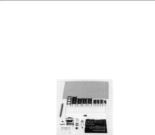
3.4Construction
Now that the parts have arrived, it is time to assemble your computer. We will start by programming the boot EPROM and the chip select PAL. Following will be a tutorial on wire-wrapping. Finally, we will lay out the components on the board and do the actual wiring.
3.4.1Programming the EPROMs
The boot ROM will give our computer a program to run every time the computer is powered up. This is possible since the boot ROM provides non-volatile storage (it doesn’t lose its memory when the power is turned off).
This step will require the use of an EPROM programmer. This might be troublesome if you don’t have access to one. Since an EPROM programmer can be an expensive item, you might want to get help from someone who owns one. The Electrical Engineering department at your local university would have one as well as your local electronics trade school. It is also possible that your local electronics repair shop would have one that you can use. If these options aren’t available to you or if you think you will be building more computers in the future, you might want to invest in your own personal EPROM programmer. Most electronics supply stores carry them. For this project, be sure that the programmer you use is able to program both EPROMs and PALs.
You can erase an EPROM by using an EPROM eraser which contains an ultraviolet lamp. The ultraviolet light is shined through the window on the chip. Never look directly at an ultraviolet lamp as it can cause serious eye damage.
Programming the Buffalo EPROM
1.Load the “buf34.s19” file into the EPROM programmer. You might have to tell it that the file is in Motorola Hex format. Specify a base address of $E000.
11
2.Program and verify the BUFFALO EPROM.
Programming the Test EPROM
1.Store the test program in Listing 1 into a text file.
Listing 1: The test program listing.
**** test.as |
**** |
|
|
RegBase |
equ |
$1000 |
|
PORTA |
equ |
$00 |
|
TCTL1 |
equ |
$20 |
|
TFLG2 |
equ |
$25 |
|
PACTL |
equ |
$26 |
|
PIA_PRA equ $A000 |
|
||
PIA_CRA equ $A001 |
|
||
PIA_PRB equ $A002 |
|
||
PIA_CRB equ $A003 |
|
||
|
org |
$E000 |
|
start |
ldx |
#RegBase |
|
|
clr |
PIA_CRA |
Initialize PIA. |
|
clr |
PIA_CRB |
|
|
ldaa |
#$FF |
|
|
staa |
PIA_PRA |
|
|
staa |
PIA_PRB |
|
|
ldaa |
#$04 |
|
|
staa |
PIA_CRA |
|
|
staa |
PIA_CRB |
|
|
ldaa |
#$80 |
|
|
staa |
PACTL,x |
|
|
clr |
TCTL1,x |
|
|
ldab |
#$38 |
Initialize test pattern. |
|
clc |
|
|
delay |
ldy |
#7 |
Wait 0.23 seconds by counting seven timer overflows. |
loop |
brclr TFLG2,x $80 loop |
Wait for timer overflow. |
|
|
ldaa |
#$80 |
|
|
staa |
TFLG2,x |
Clear timer overflow flag. |
|
dey |
|
|
|
bne |
loop |
|
|
rolb |
|
Rotate test pattern. |
|
stab |
PORTA,x |
Write test pattern. |
|
stab |
PIA_PRA |
|
|
stab |
PIA_PRB |
|
|
bra |
delay |
|
|
org |
$FFFE |
|
|
fdb |
start |
|
2.Assemble the program using the AS11 assembler.
3.Load the resulting .s19 file into the EPROM programmer as before specifying a base address of $E000.
4.Program and verify the test EPROM.
3.4.2Programming the Chip Select PAL
The Chip Select PAL (Programmable Array Logic) chip is used to perform the logic which “glues” the computer together. By using a PAL, we reduce the

12 Yerem: Build Your Own MC68HC11 Computer Trainer
number of components by eliminating many discrete logic gates. The PAL can provide much more complex designs than normally would be attempted with discrete logic. Also, if the logic needs to change, a new chip can be programmed replacing the old design.
Since all of the memory and I/O chips share the same data and address busses, they need a way to know when they are being addressed. The PAL will do this job by decoding the current value on the address bus and selecting the appropriate chip. Additionally, the PAL gates the RAM and ROM chip select signals with the E clock signal since the data bus isn’t ready until E is high. Also, the ROM chip selects are gated with the R/*W line so that the ROM is only selected during a read cycle.
Programming the PAL
1. Using a text editor, type in the program shown in Listing 2 and save i t in a text file.
Listing 2: The program listing for the Chip Select PAL.
;---------------------------------- |
|
|
Declaration Segment ------------ |
TITLE |
EVB Address Decoder |
|
|
PATTERN |
|
|
|
REVISION |
|
|
|
AUTHOR |
G. Yerem |
|
|
COMPANY |
UTK |
|
|
DATE |
|
06/19/97 |
|
CHIP |
_CSPAL PAL16L8 |
|
|
;---------------------------------- PIN Declarations --------------- |
|||
PIN |
1 |
A15 |
COMBINATORIAL ; INPUT |
PIN |
2 |
A14 |
COMBINATORIAL ; INPUT |
PIN |
3 |
A13 |
COMBINATORIAL ; INPUT |
PIN |
4 |
A12 |
COMBINATORIAL ; INPUT |
PIN |
5 |
A11 |
COMBINATORIAL ; INPUT |
PIN |
6 |
A10 |
COMBINATORIAL ; INPUT |
PIN |
7 |
RW_EN |
COMBINATORIAL ; INPUT |
PIN |
8 |
IO_EN |
COMBINATORIAL ; INPUT |
PIN |
9 |
RW |
COMBINATORIAL ; INPUT |
PIN |
10 |
GND |
; GND |
PIN |
11 |
E |
COMBINATORIAL ; INPUT |
PIN |
12 |
/RAM_SEL |
COMBINATORIAL ; OUTPUT |
PIN |
13 |
/EXTRA_SEL |
COMBINATORIAL ; OUTPUT |
PIN |
14 |
/PIA1_SEL |
COMBINATORIAL ; OUTPUT |
PIN |
15 |
/PIA2_SEL |
COMBINATORIAL ; OUTPUT |
PIN |
16 |
/RDIO_SEL |
COMBINATORIAL ; OUTPUT |
PIN |
17 |
/WRIO_SEL |
COMBINATORIAL ; OUTPUT |
PIN |
18 |
/SPARE_SEL |
COMBINATORIAL ; OUTPUT |
PIN |
19 |
/BOOT_SEL |
COMBINATORIAL ; OUTPUT |
PIN |
20 |
VCC |
; VCC |
;----- Boolean Equation Segment. ---- |
|
|
|
EQUATIONS |
|
|
|
RAM_SEL |
= (/A15)*E |
; $0000 - $7FFF |
|
EXTRA_SEL |
= ( A15*/A14*/A13)*E*RW |
; $8000 - $9FFF |
|
PIA1_SEL |
= ( A15*/A14* A13*/A12*/A11*/A10) |
; $A000 - $A3FF |
|
PIA2_SEL |
= ( A15*/A14* A13*/A12*/A11* A10) |
; $A400 - $A7FF |
|
RDIO_SEL |
= ( A15*/A14* A13*/A12* A11*/A10 + IO_EN)*(E* RW + RW_EN) |
; $A800 |
- $ABFF |
WRIO_SEL |
= ( A15*/A14* A13*/A12* A11* A10 + IO_EN)*(E*/RW + RW_EN) |
; $AC00 - $AFFF |
|
SPARE_SEL |
= ( A15* A14*/A13)*E*RW |
; $C000 |
- $DFFF |
BOOT_SEL |
= ( A15* A14* A13)*E*RW |
; $E000 |
- $FFFF |

13
2.Using PALASM or a similar program, compile the PAL program to generate a JEDEC file. (PALASM is a freeware program from AMD which runs under DOS.)
3.Using an EPROM programmer, program the PAL using the JEDEC file.
You can test your PAL by placing it in a solderless breadboard and examining the outputs for different input combinations.
3.4.3Board Layout
The next step is to lay out the components on the board.
First place the sockets and discrete components on the perfboard. The scale drawing in Appendix 2 offers a suggested layout. Keep in mind that the DIP wire-wrap sockets have an indentation which marks pin 1 of the chip. The indentation on the socket corresponds to the indentation on the chip itself.
Next label the underside of the board. This will prevent errors when you are wiring the board. It can be very frustrating to finish wiring a project, only to find out that you’ve wired the chips backwards. White adhesive correction tape, which can be found at office supply stores, works good for this purpose. Also, you can buy preprinted labels for wire-wrapping if you don’t want to make the labels yourself. For this project, Appendix 4 has some pre-printed labels that you can cut out and glue to the board.
Now remove the discrete components and carefully turn the board over. Cut out the labels in Appendix 4 and glue them underneath the appropriate sockets. A knife and tweezers are helpful for placing the labels. Also, double check to make sure you have the orientations correct.