


28 Yerem: Build Your Own MC68HC11 Computer Trainer
5.1.1Using BUFFALO
The BUFFALO monitor program will allow you to do most of your program development. In BUFFALO you can view and modify memory and registers, assemble and disassemble programs, and perform advanced debugging. The most important feature of BUFFALO is its Load command. It allows you to download Motorola Hex (.s19) files to the computer’s RAM through the serial port. Here is a procedure for using BUFFALO in your program development:
1.Write the source code.
2.Give the source code a base address somewhere in the RAM’s address space between $0000 - $7FFF (watch out for the MC68HC11’s Control Registers).
3.Cross-compile your program as an .s19 file.
4.At the BUFFALO prompt, type: load t [ENTER]. Now BUFFALO will wait to receive a .s19 byte stream over the serial port. Use your terminal emulator program to send the .s19 text file to BUFFALO.
5.If everything goes well, BUFFALO will print the message: done and provide the command prompt again.
6.You can now run your program by using the go command.
If you forget a command in BUFFALO, typing: help [ENTER] will display the list of commands. The EVB manual has detailed descriptions of the other BUFFALO commands.
5.1.2Programming Your Own ROMs
You can write your program to fit in a boot ROM. First you have to place the program in the space between $E000 - $FFFF and place a jump vector to your program in the address $FFFE. When your new ROM is programmed you must physically remove the BUFFALO ROM and replace it with your new ROM. Subsequently, your new program will run every time the computer is turned on.
Alternately, you can use the Spare ROM socket for your program. In this case you must place your program within the space $C000 - $DFFF. This time though, you won’t be able to modify the Reset jump vector to jump to your program. You can either run your program from the BUFFALO prompt, or pull the J4 jumper high to tell BUFFALO to jump to the first location of the MC68HC11’s internal EEPROM at $B600. Then you simply need to put a jump instruction at $B600 to call your new program. Keep in mind that the Spare ROM socket is for your use and can be left empty most of the time.
Most of the time though, you will be loading your program into the computer’s RAM and executing the program from there. The advantage of this is that you will be able to rapidly change your program and try it out. The disadvantage is that the program will disappear when the computer is turned off.
5.2Interfacing
In order to keep the design practical certain built-in resources of the MC68HC11 aren’t available on our computer. For example, in this design the pins PD0 and PD1 are used for the serial port and as a result aren’t readily available for use as digital I/O. Also, since the BUFFALO monitor program uses PE0 as an input

29
for the J4 jumper, PE0 shouldn’t be used for other purposes. Additionally, lines PE4 through PE7 of Port E aren’t pinned out on the MC68HC11A1P version used in this design. This is because the DIP (Dual Inline Package) version of the MC68HC11A1 used here doesn’t have enough pins to accommodate all of Port E. The pins PE4 through PE7 are only available on the PLCC (Plastic Leaded Chip Carrier) version. The PLCC version wasn’t used for this project because i t would have been harder to wire by hand. Finally, Port B, Port C, STRA and STRB are unavailable because we are operating the MC68HC11 in expanded mode as opposed to single chip mode. Expanded mode is what allows us to connect external memory like the HM62256 RAM chip and the 27C64 EPROM chip to the microprocessor.
Despite these limitations, expanded mode allows us to add as much I/O to the computer as we require, albeit with a few extra chips required. In this design, the MC68B21 chip augments the available digital I/O. The following sections will describe how to use the MC68B21 and how add even more digital I/O to the design.
5.2.1How to use the MC6821
The MC6821 Peripheral Interface Adapter (PIA) chip provides bi-directional digital I/O for the 6800 family of microprocessors with a minimum of fuss. The MC6821 has two bi-directional 8-bit data ports along with two handshaking control lines for each port. The handshaking lines allow each port to be used as parallel communication ports.
|
|
|
(U2) |
Vcc |
||
|
|
MC68B21 |
||||
|
|
|
|
|||
D7 |
2 6 |
D7 |
CS1 2 4 |
|
||
D6 |
2 7 |
|
2 2 |
|
||
D5 |
2 8 |
D6 |
CS0 3 5 |
A1 |
||
D4 |
2 9 |
D5 |
RS1 3 6 |
A0 |
||
D3 |
3 0 |
D4 |
RS0 |
2 3 |
*PIA1 ($A000) |
|
D3 |
*CS2 |
|||||
D2 |
3 1 |
2 5 |
E |
|||
E |
||||||
D1 |
3 2 |
D2 |
|
2 1 |
R/*W |
|
D0 |
3 3 |
D1 |
R/*W |
3 4 |
*RESET |
|
|
|
D0 |
*RESET |
|
|
|
CA2 |
3 9 |
CA2 |
CB2 1 9 |
CB2 |
||
CA1 |
4 0 |
CA1 |
CB1 1 8 |
CB1 |
||
PPA7 |
9 |
PA7 |
PB7 |
1 7 |
PPB7 |
|
PPA6 |
8 |
1 6 |
PPB6 |
|||
PPA5 |
7 |
PA6 |
PB6 |
1 5 |
PPB5 |
|
PA5 |
PB5 |
|||||
PPA4 |
6 |
PA4 |
PB4 |
1 4 |
PPB4 |
|
PPA3 |
5 |
PA3 |
PB3 |
1 3 |
PPB3 |
|
PPA2 |
4 |
1 2 |
PPB2 |
|||
PPA1 |
3 |
PA2 |
PB2 |
1 1 |
PPB1 |
|
PPA0 |
2 |
PA1 |
PB1 |
1 0 |
PPB0 |
|
PA0 |
PB0 |
|||||
Internally, the MC6821 has six registers for operating the chip, three registers for Port A and three registers for Port B. When RS1=0 the Port A register set is selected and when RS1=1 the Port B registers are selected. When RS0=1 the Control Register for the given port is selected. When RS0=0 the register that is accessed depends on bit 2, the DDR Access Bit, of the Control Register. If the DDR Access Bit is 0, the Data Direction Register is selected. If the DDR Access Bit is 1, the Peripheral I/O Register is selected.
The MC6821 Control Register
b7 |
b6 |
b5 |
b4 |
b3 |
b2 |
b1 |
|
b0 |
IRQ A(B) 1 |
IRQ A(B) 2 |
|
CA2 (CB2) |
|
DDR |
|
CA1 (CB1) |
|
Flag |
Flag |
|
Control |
|
Access |
|
Control |
|
30 Yerem: Build Your Own MC68HC11 Computer Trainer
The Data Direction Register for each port allows any of the lines on a port to be configured as inputs or outputs. A zero bit will configure a line as an input while a one bit will configure the line as an output. Similarly, the Peripheral I/O Register allows you to read from and write to the I/O ports.
A simple procedure for programming a port on the MC6821 is to:
1.Set the DDR Access Bit in the Control Register to 0.
2.Program the Data Direction Register.
3.Set the DDR Access Bit in the Control Register to 1.
4.Access the Peripheral I/O Register to read and write the I/O port.
This procedure applies for both Port A and Port B. Once you have programmed the Data Direction Register, you probably will want to leave the DDR Access Bit set to 1 for the rest of the program.
Here is a code snippet which demonstrates how to program the MC6821:
clr |
$A001 |
Set the DDRA Access Bit to 0. |
clr |
$A003 |
Set the DDRB Access Bit to 0. |
ldaa #FF |
|
|
staa $A000 |
Set all bits on Port A to output. |
|
ldaa #0F |
|
|
staa $A002 |
Set upper bits of Port B to input and lower bits to output. |
|
ldaa #04 |
|
|
staa $A001 |
Set the DDRA Access Bit to 1. |
|
staa $A003 |
Set the DDRB Access Bit to 1. |
|
ldaa #FF |
|
|
staa $A000 |
Turn on all of the bits on Port A. |
|
ldaa $A002 |
Read Port B. |
|
Check the |
MC6821 data sheet to find out how to use its more advanced |
|
features.
5.2.2Adding a Basic Input Port
If you need digital inputs, the following one chip circuit will do the job,
|
|
|
|
74HC244 |
||
|
|
D7 |
3 |
2Y4 |
2A4 |
|
|
Bus |
D6 |
5 |
2Y3 |
2A3 |
|
|
D5 |
7 |
||||
|
D4 |
9 |
2Y2 |
2A2 |
||
Bus |
Data |
|||||
D3 |
1 2 |
2Y1 |
2A1 |
|||
|
|
|
|
|||
Control |
|
D2 |
14 |
1Y4 |
1A4 |
|
|
D1 |
16 |
1Y3 |
1A3 |
||
|
|
D0 |
18 |
1Y2 |
1A2 |
|
|
|
1Y1 |
1A1 |
|||
|
|
|
|
|||
|
|
|
19 |
*2G |
|
|
|
*RDIO ($A800) |
1 |
|
|||
|
*1G |
|
||||
|
|
|
|
|
||
1 7
In7
1 5
In6
1 3
In5
1 1
In4
8
In3
6
In2
4
In1
2
In0
Vcc - Pin 20
Gnd - Pin 10
To read the current state of the input lines simply perform a read from the address $A800. The following line of assembly language will read the values of the eight input lines into the A register:
ldaa $A800
This circuit can apply to other type of digital input that you would want to connect to the computer, such as an analog-to-digital converter.
31
5.2.3Adding a Basic Output Port
Here is a circuit similar to the previous one which provides eight digital outputs to the computer,
|
|
|
|
74HC273 |
||
|
|
D7 |
1 8 |
8D |
8Q |
|
|
Bus |
D6 |
1 7 |
7D |
7Q |
|
|
D5 |
1 4 |
||||
|
D4 |
1 3 |
6D |
6Q |
||
Bus |
Data |
|||||
D3 |
8 |
5D |
5Q |
|||
|
|
|
|
|||
Control |
|
D2 |
7 |
4D |
4Q |
|
|
D1 |
4 |
3D |
3Q |
||
|
|
D0 |
3 |
2D |
2Q |
|
|
|
1D |
1Q |
|||
|
|
|
|
|||
|
*RESET |
1 |
*CLR |
|
||
|
*WRIO |
11 |
|
|||
|
|
|
||||
CLK
1 9
Out7
1 6
Out6
1 5
Out5
1 2
Out4
9
Out3
6
Out2
5
Out1
2
Out0
Vcc - Pin 20
Gnd - Pin 10
A simple write to the address $AC00 will change the states of the outputs. The following two lines of assembly language show how to do this:
ldaa #AA staa $AC00
You can of course use this circuit as an example for connecting other types of output devices to the computer.
5.2.4Adding More PIAs
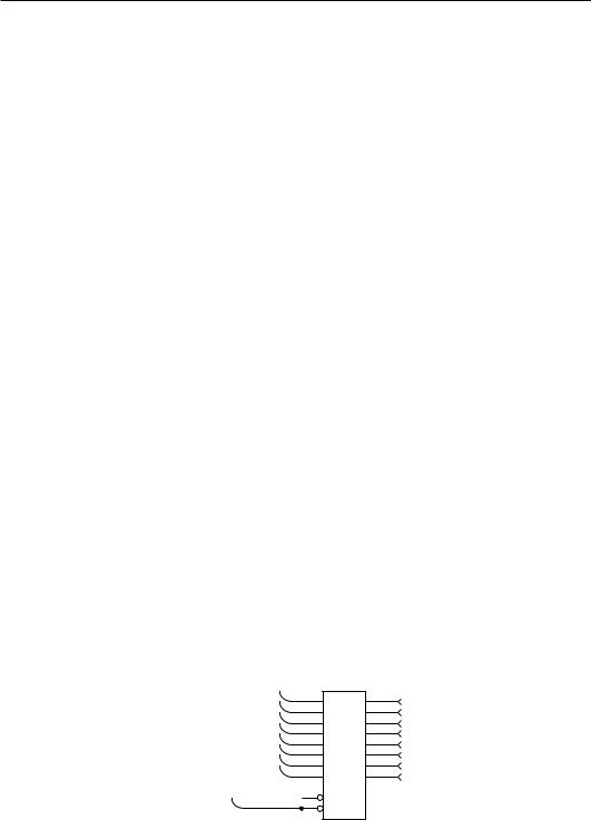
If you require more sophisticated I/O, you can add more PIAs to the computer. Simply plug the new PIA into the breadboard and wire it directly to the data bus through the terminal strip. The only difference between the second PIA and the original one is that the *CS2 pin of the new PIA is connected to the *PIA2 signal. This means that the base address of the new PIA begins at $A400 instead of $A000.
Data Bus
|
|
|
|
|
|
MC68B21 |
Vcc |
|||||||
|
|
|
|
|
|
|
|
|
|
|
|
|
||
D7 |
26 |
|
|
24 |
|
|
|
|
|
|
||||
D7 |
CS1 |
|
|
|
|
|
|
|||||||
D6 |
27 |
22 |
|
|
|
|
|
|
||||||
CS0 |
|
|
|
|
|
|
||||||||
D5 |
28 |
D6 |
35 |
|
|
A1 |
||||||||
|
|
|
||||||||||||
|
|
|
|
|
|
D5 |
RS1 |
|
|
|
|
|
|
|
D4 |
29 |
36 |
|
|
A0 |
|
||||||||
|
|
|
|
|
|
D4 |
RS0 |
|
|
|
|
|
|
|
D3 |
30 |
23 |
|
|
|
|
|
|
||||||
|
|
|
|
|
|
D3 |
*CS2 |
|
|
|
|
|
|
|
D2 |
31 |
25 |
|
|
|
|
|
|
||||||
D2 |
E |
|
|
|
|
|
|
|||||||
D1 |
32 |
R/*W |
21 |
|
|
|
|
|
|
|||||
|
|
|
|
|
|
D1 |
|
|
|
|
|
|
|
|
D0 |
33 |
34 |
|
|
|
|
|
|
||||||
|
|
|
|
|
|
|
||||||||
|
|
|
|
|
|
D0 |
*RESET |
|
|
|
|
|
|
|
|
|
|
|
|
39 |
19 |
|
|
|
|
|
|
||
|
|
|
|
|
CA2 |
CB2 |
|
|
|
|
|
|
||
|
|
|
|
|
40 |
CA1 |
CB1 |
18 |
|
|
|
|
|
|
|
|
|
|
|
|
|
|
|
|
|
||||
|
|
|
|
|
9 |
17 |
|
|
|
|
|
|
||
|
|
|
|
|
PA7 |
PB7 |
|
|
|
|
|
|
||
|
|
|
|
|
|
|
|
|
|
|
||||
|
|
|
|
|
|
|
|
|
|
|
|
|
||
|
|
|
|
|
8 |
16 |
|
|
|
|
|
|
||
|
|
|
|
|
|
|
|
|
|
|
||||
|
|
|
|
|
|
PA6 |
PB6 |
|
|
|
|
|
|
|
|
|
|
|
|
7 |
15 |
|
|
|
|
|
|
||
|
|
|
|
|
|
|
|
|
|
|
||||
|
|
|
|
|
|
PA5 |
PB5 |
|
|
|
|
|
|
|
|
|
|
|
|
6 |
14 |
|
|
|
|
|
|
||
|
|
|
|
|
PA4 |
PB4 |
|
|
|
|
|
|
||
|
|
|
|
|
|
|
|
|
|
|
||||
|
|
|
|
|
|
|
|
|
|
|
||||
|
|
|
|
|
5 |
13 |
|
|
|
|
|
|
||
|
|
|
|
|
PA3 |
PB3 |
|
|
|
|
|
|
||
|
|
|
|
|
|
|
|
|
|
|
||||
|
|
|
|
|
|
|
|
|
|
|
||||
|
|
|
|
|
4 |
12 |
|
|
|
|
|
|
||
|
|
|
|
|
PA2 |
PB2 |
|
|
|
|
|
|
||
|
|
|
|
|
|
|
|
|
|
|
||||
|
|
|
|
|
|
|
|
|
|
|
|
|
||
|
|
|
|
|
3 |
11 |
|
|
|
|
|
|
||
|
|
|
|
|
|
|
|
|
|
|
||||
|
|
|
|
|
|
PA1 |
PB1 |
|
|
|
|
|
|
|
|
|
|
|
|
2 |
10 |
|
|
|
|
|
|
||
|
|
|
|
|
|
|
|
|
|
|
||||
|
|
|
|
|
|
PA0 |
PB0 |
|
|
|
|
|
|
|
|
|
|
|
|
|
|
|
|
|
|
|
|
||
|
|
|
|
|
|
|
|
|
|
|
|
|
|
|
|
|
|
|
|
|
|
|
|
|
|
|
|
|
|
Bus Address |
Bus Control |
*PIA2 ($A400) E R/*W *RESET
Vcc - Pin 20
Gnd - Pin 1
Now you have two extra bi-directional ports to work with. Similarly, you can add as many PIAs to the computer as you need, keeping in mind that there are only a finite number of unused address locations available.