

ivchenko_bookreg
.pdf
|
|
4.3 |
Intrasubband Optical Transitions |
191 |
||||
|
|
η = |
ω |
|
W |
(4.44) |
||
|
|
I |
||||||
|
|
|
|
|
|
|
||
can be expressed in terms of current and field, and be written as |
|
|||||||
η = |
2 |
Re ,j (ω) · E (ω)' |
= |
4πe2N2Dγ |
(4.45) |
|||
|
|
. |
||||||
I |
m cnω (ω2 + γ2) |
|||||||
Here W is the photon absorption rate and I = (cnω /2π)|E (ω)|2 is the light intensity.
¯ |
|
|
|
For ω E, the expression for η can be derived by solving the kinetic |
|||
equation |
|
δfk(ω) |
|
−iω δfk(ω) + |
e |
|
|
E · kf 0(Ek) + |
τp |
= 0 |
|
for the deviation of the electron distribution function, δfk, induced by the in-plane electric field. The result coincides with (4.45) if γ−1 is set equal to the momentum scattering time.
In the limit ω τp−1 the absorption rate W (or absorbance η) can be calculated by using Fermi’s golden rule for indirect transitions. For scattering by static defects this rule reads
W = |
2π 2πe2I 2 |
|
|
R(i) |
2 |
(fk0 |
|
fk0 )δ(Ek |
|
Ek |
|
ω) |
(4.46) |
||||
|
|
|
|
|
|
|
|
|
|
||||||||
ω2cnω S |
|
| |
| |
− |
− |
− |
|||||||||||
|
k k |
k k |
|
|
|
|
|
||||||||||
|
|
|
|
|
|
i |
|
|
|
|
|
|
|
|
|
|
|
|
|
|
|
|
|
|
|
|
|
|
|
|
|
|
|
|
|
with the second-order matrix element for defect-assisted electron-photon interaction being
R(i) |
= |
(e · vk )Vk(ik) |
+ |
Vk(ik) (e · vk) |
|
|||||
k k |
|
Ek |
− |
Ek |
|
ω |
|
|||
|
|
|
|
|
|
|
|
− |
|
|
|
= |
Vk(ik) |
|
|
|
|||||
|
|
|
|
|
|
e · (k − k) . |
(4.47) |
|||
|
m |
ω |
|
|||||||
Here vk = k/m is the electron velocity, Vk(ik) is the matrix element of spin-conserving elastic scattering k → k and the index i enumerates the elementary scatterers. The corresponding momentum relaxation time that determines the mobility is given by
2π 2 = S k i
where θ is the scattering angle. Further analysis is readily performed assuming Vk(ik) is k and k independent which is valid for defects with a short-range inplane scattering potential. Then the absorbance in the high-frequency limit can be presented as
η = |
4πe2N2D γ(ω) |
, |
(4.48) |
|
m cnω ω2 |
||||
|
|
|

192 4 Intraband Optical Spectroscopy of Nanostructures
where γ is a function of the light frequency. In accordance with the kinetic-
¯
theory result, at low frequencies, i.e. for ω E, the damping γ coincides
−1 ¯
with τp , while in the high-frequency region, ω E but ω < E21, the damping constant becomes (2τp)−1.
For intrasubband optical transitions assisted by phonons, the transition
probability rate is similar to (4.46) |
|
|
|
|
|
|
|
||||||||||
W = |
2π 2πe2I 2 |
|
Rk k(q) 2 |
δ(Ek Ek ω Ωq ) |
|
(4.49) |
|||||||||||
|
|
|
|
|
|
|
|
|
| |
|
| |
− − ± |
|
|
|
|
|
|
|
ω2cnω S |
k k q, |
± |
|
|
|
|
|||||||||
|
|
|
|
|
|
|
|
+ 2 ± |
2 |
|
− fk (1 − fk) mq + 2 |
2 |
. |
||||
|
× fk(1 − fk ) mq |
|
|||||||||||||||
|
|
|
|
|
|
|
|
|
1 |
|
1 |
|
|
1 |
|
1 |
|
Here fk is the electron distribution function, the sign + or − indicates the process of phonon emission or absorption, q, Ωq and mq are the phonon wave vector, frequency and occupation number, respectively. For equilibrium phonons the latter is described by the Planck function [exp ( Ωq /kB T )−1]−1. The matrix element of the indirect electron-photon interaction is presented in the form
|
|
(e vk )Vk±k(q) |
|
Vk±k(q)(e |
|
vk) |
|||||||
Rk k(q) = |
· |
Ωq |
+ |
|
|
− ω |
· |
|
δk ±q ,k |
||||
Ek − Ek ± |
|
|
|
||||||||||
|
Vk±k |
|
|
|
|
|
|
|
|
||||
= |
|
|
|
e · (k − k) δk ±q ,k , |
|
(4.50) |
|||||||
m |
ω |
|
|||||||||||
where Vk±k(q) is the matrix element of electron-phonon interaction, and the δ-symbol describes the in-plane momentum conservation in the scattering act. The first term in the right-hand side of (4.50) corresponds to the process of electron scattering by a phonon to the virtual state k followed by absorption of a photon while the second term describes the transition where the photon absorption precedes the scattering by a phonon.
The main features of the phonon-assisted intrasubband absorption can be understood neglecting interface e ects on the phonon energy spectrum and treating the electron-phonon interaction as that between 2D electrons and conventional 3D phonons. Then for the matrix element of electron interaction with polar-optical phonons in a zinc-blende QW structure one has
k k |
± | | |
V0(q2 + qz2) |
æ∞ − æ0 |
|
1/2 |
|
|||||
V ± (q) = |
i e |
|
2π ΩLO |
1 |
|
1 |
|
J(±)(qz ) , |
(4.51) |
||
|
|
|
|
|
|
|
|
||||
where |
J(+)(qz ) = J(−) (qz ) = |
|
|
|
|
|
|||||
|
e−iqz z ϕe21(z) dz |
(4.52) |
|||||||||
and ϕe1(z) is the envelope function of a quantum-confined electron. In symmetrical QWs, J(+)(qz ) and J(−)(qz ) coincide and are real. A similar form has the matrix element for deformation-potential or piezoelectric interaction of

4.3 Intrasubband Optical Transitions |
193 |
electrons with acoustic phonons. Particularly, for the deformation-potential interaction one has
|
|
|
|
|
|
|
|
1/2 |
|
|
Vk±k(q) = |
|
|
q2 |
+ qz2 |
|
|
||||
i Ξc |
J(±)(qz ) , |
(4.53) |
||||||||
s |
|
|||||||||
|
|
|
0 |
|
LA |
|
|
|
||
where Ξc is the deformation-potential constant, ρ is the density of the semiconductor and sLA is the longitudinal sound velocity.
In a symmetric QW with infinitely high barriers, the integral (4.52) equals
to
J(±)(qz ) = x |
1 + π2 − x2 , |
||
|
sin x |
|
πx |
where x = qz a/2. Values of [J(±)(qz )]2 are close to unity for x < π/2 and become negligible for x > 3π/2. Therefore, a typical value of qz in (4.53) is π/a while
|
2 |
2m |
¯ |
|
|
|
|
|
||
|
q |
|
|
|
max E, ω . |
|
|
|
|
|
|
|
2 |
|
|
|
|
||||
This di ers from intraband optical transitions |
in a bulk semiconductor where |
|||||||||
2 |
2 |
2 |
is determined by max |
|
¯ |
|
||||
the square modulus qx + qy |
+ qz |
|
E, ω . |
|||||||
Figure 4.8 presents the calculated temperature |
dependence of the absorp- |
|||||||||
|
|
|
|
|||||||
tion coe cient of GaAs/AlGaAs MQWs, K = η/d, at the wavelength λ = 92 µm ( ω = 13 meV) [4.11]. One can see the separate contributions to indirect absorption due to scattering by optical phonons, impurities and interface imperfections as well as a sum of these contributions.
Since the LO-phonon energy ΩLO in GaAs is 36 meV and ω < ΩLO, at low temperatures the light absorption of electrons interacting with LOphonons can be ignored and the scattering by static defects is dominating. With increasing temperature the role of transitions accompanied by LOphonon absorption increases. At the same time the step-like energy distribution of the degenerate 2D electron gas is smeared, and photon absorption followed by emission of a LO phonon also becomes possible. As a result, the optical-phonon assisted absorption is dominating starting with T = 200 K.
Agethe and Vass [4.12] have calculated the LO-phonon limited intrasubband photon absorption in n-doped QWs taking into account that the actual phonon spectrum is more complicated and consists of confined, interface (symmetric and antisymmetric), half-space and bulk modes. They analyzed the contribution to the absorption from each phonon mode as a function of four controllable parameters, namely, the light frequency ω, QW thickness a, electron temperature Te and density N2D.
4.3.2 Electron Cyclotron Resonance in a Superlattice
Cyclotron resonance is the most powerful technique for measuring the e ective masses in solids. In the classical description of the cyclotron resonance

194 4 Intraband Optical Spectroscopy of Nanostructures
) |
4000 |
|
λ = 92 µm |
|
|
|
-1 |
|
|
|
|||
Κ (cm |
|
|
T = 4.2 K |
|
|
|
|
|
|
|
|
|
|
coefficient, |
3000 |
|
|
|
|
|
|
|
|
|
|
Sum |
|
|
Interface |
Nonequilibrium |
||||
|
roughness |
|||||
2000 |
|
phonons |
||||
Absorption |
|
|||||
|
|
|
||||
1000 |
Impurity |
|
|
Equilibrium |
||
|
|
|
||||
|
|
|
|
phonons |
||
|
|
|
|
|
||
|
0 |
100 |
|
200 |
300 |
400 |
|
|
|
||||
Electron temperature, Te (K)
Fig. 4.8. Calculated contributions of various scattering mechanisms to the farinfrared absorption coe cient of a biased n-doped GaAs/AlGaAs MQW structure for s-polarized light. In the calculation, interface scattering, impurity scattering, scattering by equilibrium and nonequilibrium phonons are taken into account. The sum of all contributions is shown by the solid line. From [4.11].


4.3 Intrasubband Optical Transitions |
197 |
˚
optically detected cyclotron resonance in a structure consisting of 180-A-
˚
thick GaAs wells separated by 230-A Al0.33Ga0.67As barriers [4.13]. These indirect methods for observing cyclotron and magnetic resonances, Optically Detected Cyclotron Resonance (ODCR) and Optically Detected Magnetic Resonance (ODMR), involve the monitoring of microwave-induced changes in the luminescence intensity.
In the case of SLs, coupling between wells through thin penetrable barriers transforms subbands of electron quantum-confined states into minibands of extended states. The energy dispersion of the latter has a 3D character. Therefore, the cyclotron resonance in SLs should reveal properties similar to those in a uniaxial semiconductor crystal with the longitudinal e ective mass drastically dependent on the barrier thickness. Particularly, the Landau levels are formed not only in the B z geometry as in the case of QWs but also in a magnetic field lying in the interface plane. According to (4.60), in the latter configuration the cyclotron mass is the geometric mean of the in-plane mass mt and the “superstructural” mass ml, and the spacing between Landau levels is smaller than in the former configuration. Landau levels in a SL were first observed in both configurations of the magnetic field by Belle et al. [4.14] who studied the photoluminescence excitation spectra of the structure con-
˚ |
˚ |
taining 40 periods of 39.2-A |
GaAs wells and 11.2-A Al0.4Ga0.6As barriers. |
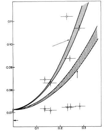
The first direct cyclotron-resonance measurements on extended states in a semiconductor SL were performed by Du eld et al. [4.15]. Figure 4.9 illustrates their measurements of the normal (ml) and in-plane (mt) e ective masses in a GaAs/AlxGa1−xAs as a function of the aluminum fraction x in the barriers. The curves bounding the shaded areas represent the ml(x) dependence calculated for a SL with rectangular wells and barriers, and for the conduction-band o set V = 0.65∆Eg or V = 0.61∆Eg using the KronigPenney boundary conditions
ϕA = ϕB , |
dϕ |
= |
dϕ |
(4.65) |
|
|
|
||||
dz |
dz |
||||
|
A |
B |
|||
|
|
|
or the Bastard boundary conditions (2.10).
The above picture of the cyclotron orbits in the geometry B x2 is valid at low magnetic fields when the magnetic length λB,z is larger than the SL period d, and an electron can complete its elliptical cyclotron orbit through several barriers. If the lattice periodicity and cyclotron orbit radius are comparable the electron energy gets dependent on the position of the cyclotron orbit along the growth axis z and one needs to solve explicitly the Schr¨odinger equation for the electron envelope function ψ(r) in a SL [4.16]. With B y and using the Landau gauge, Ax = Bz, Ay = Az = 0, this function can be sought in the form
ψ(r) = ei(kx x+ky y)ϕ(z) , |
(4.66) |
where ϕ(z) satisfies the equation
198 4 Intraband Optical Spectroscopy of Nanostructures
Bastard
Mass
Kronig-Penney
Aluminum fraction in barrier
Fig. 4.9. E ective electron mass related to the free electron mass in the lowest
˚ ≈ ˚
miniband e1 in GaAs/AlxGa1−xAs SL with a = 80 A, b 20 A vs. composition x. The experimental data were obtained from a cyclotron resonance study. Circles, the normal mass ml ≡ mzz ; triangles, the in-plane mass mt ≡ mxx = myy . The calculations performed for the boundary conditions (4.65) and (2.10) are displayed by shaded areas. The curves bounding these areas correspond to the conductionband o set V = 0.65∆Eg (top curve) and V = 0.61∆Eg (bottom curve). From [4.15].
2 |
kx − |
eB |
|
2 |
ϕ(z) − |
d 2 d |
|
|||||
z |
+ ky2 |
ϕ(z) + V (z)ϕ(z) = Eϕ(z) . |
||||||||||
2m |
c |
dz |
|
2m |
|
dz |
||||||
Here the notations x, y, z are used instead of x1, x2, x3, V (z) is the superstructure potential, and the e ective mass m is allowed to be di erent in the well and barrier materials. The position of the cyclotron orbit z0 = kxλ2B is a good quantum number. In the limit λB,z = (mt/ml)1/4λB d, the Landau levels are flat, i.e., they have the same energy for all values of z0. At

4.4 Infrared Reflection from Quantum Wells and Superlattices |
199 |
higher fields, as the cyclotron energy approaches the miniband width, λB,z and d become comparable and the interlevel energy spacing as a function of B tends to saturate. Simultaneously, the Landau levels develop dispersion, and the resonant absorption spectrum broadens [4.17].
4.4 Infrared Reflection from Quantum Wells and Superlattices
Optical phonon modes dominate the infrared absorption and spectroscopic ellipsometry in undoped bulk semiconductors and multi-layered heterostructures. Infrared reflectance can be used as a simple, contactless and nondestructive, characterization technique to provide the information on the thicknesses of the various layers, alloy composition, phonon frequencies and broadening parameters. We consider here the infrared reflection spectroscopy from an undoped SL and its description in the e ective-medium dielectric function model.
For a crystal of cubic symmetry with two di erent atoms in the unit cell, the dielectric function in the infrared region can be represented in the form
æ(ω) = æ |
ΩL2 |
− ω2 |
− 2iΓLω |
, |
(4.67) |
|
∞ ΩT2 − ω2 − 2iΓT ω |
||||||
|
|
|
||||
where ΩL and ΩT are the resonance frequencies of the LO and TO phonon, respectively, æ∞ is the high-frequency dielectric constant, and ΓL, ΓT are the phonon damping rates. In general, ΓL = ΓT but usually these constants are assumed to coincide.
Let a SL consist of alternating layers of semiconductors A and B with the isotropic dielectric functions æA(ω) and æB(ω), described by (4.67) with a given set of parameters æ∞A , ΩT 1, ΩL1 for the layer A, and æ∞B , ΩT 2, ΩL2 for the layer B. For simplicity, in the main part of this section, we neglect the phonon damping. For an arbitrary relation between the light wavelength and the SL period d = a+b, one needs to use the straightforward treatment of the normal light waves in a periodic medium presented in Chap. 2. If the light wavelength is large compared to the SL period d = a + b, then, according to (2.132), the SL may be treated as a homogeneous uniaxial medium with two linearly independent components of the dielectric tensor,
æ (ω) ≡ æxx = æyy = |
æA(ω)a + æB(ω)b |
, |
(4.68) |
||
a + b |
|||||
æ (ω) ≡ æzz = |
(a + b)æA(ω)æB(ω) |
|
|
||
|
. |
|
|
||
æA(ω)b + æB(ω)a |
|
|
|||
The function æ (ω) has poles at the points ω = ωT 1, ωT 2 and the function æ (ω) has zeros at the points ω = ωL1, ωL2. Denoting the zeroes of the function

200 4 Intraband Optical Spectroscopy of Nanostructures
æA(ω)a + æB(ω)b
by ω ,1, ω ,2 and those of the function
æA(ω)b + æB(ω)a
by ω ,1, ω ,2 we can represent the frequency dependence of the components
(4.68) |
in a factorized form |
|
|
|
|
|
|
|
||
|
æ |
(ω) = æ∞ |
(ω2 ,1 − ω2)(ω2 ,2 − ω2) |
, |
(4.69) |
|||||
|
|
|
|
(ΩT2 1 − ω2)(ΩT2 2 − ω2) |
|
|
||||
|
æ |
(ω) = æ∞ |
(ΩL2 1 − ω2)(ΩL2 2 − ω2) |
, |
|
|||||
where |
|
|
|
(ω2,1 − ω2)(ω2,2 − ω2) |
|
|
||||
|
|
æ∞a + æ∞b |
|
(a + b)æ∞æ∞ |
|
|||||
|
æ∞ = |
, æ∞ = |
(4.70) |
|||||||
|
A |
B |
|
A |
B . |
|||||
|
|
|
|
|
|
|||||
|
|
|
|
a + b |
|
æA∞b + æB∞a |
|
|||
Note that in a SL with layers of equal thicknesses, a = b, the frequencies ω ,j and ω ,j coincide.
In a uniaxial medium, solutions of the Maxwell equations split into ordinary and extraordinary waves. For the ordinary waves (s- or TE-polarization), the electric vector E is perpendicular to the plane containing the light wave vector q and the principal axis. The dispersion equation has the form
q2 =
ω 2
c
For the extraordinary waves (p- or TM-polarization), the vector E lies in the plane (q, z), and the dispersion equation is
q2 = ω 2 æ (ω)æ (ω) ,
cæ (ω) cos2 θ + æ (ω) sin2 θ
where θ is the angle between q and z. For the reflection coe cient from the boundary between the vacuum and semi-infinite SL, one obtains
Rµ = |rµ|2 , rµ = 1 − n¯µ ,
1 + n¯µ
where the index µ = s, p indicates the polarization of the incident wave,
|
æ |
sin2 θ0 |
|
1/2 |
|
1 |
|
æ − sin2 |
θ0 |
1/2 |
|
|
|
|
|
|
|
|
|||||||
n¯s = |
|
−cos θ0 |
|
|
, n¯p = |
|
|
|
|
|
, |
(4.71) |
|
cos θ0 |
æ æ |
|
|||||||||
and θ0 is the external angle of incidence.
If a SL is finite and grown on a substrate with an isotropic dielectric constant æb, one has to take into account the light reflection at the boundary