

Broadband Packet Switching Technologies
.pdf86 SHARED-MEMORY SWITCHES
Fig. 4.3 Two linked-list logical queues.
and a stream of the corresponding headers to the route decoder ŽRT DEC. for maintaining logical queues. The RT DEC then decodes the header stream one by one, accesses the corresponding tail pointer register ŽTPR., and triggers the WRITE process of the logical queue. An idle address of the cell memory is simultaneously read from an idle address FIFO ŽIAF. that holds all vacant cell locations of the shared memory.1 This is the next-address pointer in the cell memory, pointing to the address for storing the next arriving cell. This address is also put into the corresponding TPR to update the logical queue. Figure 4.3 shows two logical queues, where next pointers ŽNPs. are used to link the cells in the same logical queue. TPR 0 and head pointer register ŽHPR. 0 correspond to output port 0, where n y 1 cells are linked together. TPR 1 and HPR 1 correspond to output port 1, The end of each logical queue indicates the address into which the next cell to the output will be written.
The READ process of the switch is the reverse of the WRITE process. The cells pointed to by the HPRs Žheads of the logical queues. are read out of the memory one by one. The resulting cell stream is demultiplexed into the outputs of the switch. The addresses of the leaving cells then become idle, and will be put into the IAF.
1 Since FIFO chips are more expensive than memory chips, an alternative to implementing the IAF is to store vacant cells’ addresses in memory chips rather than in FIFO chips, and link the addresses in a logical queue. However, this approach requires more memory access cycles in each cell slot than using FIFO chips and thus can only support a smaller switch size.

LINKED-LIST APPROACH |
87 |
Fig. 4.4 Adding and deleting a cell in a logical queue for the tail pointer pointing to a vacant location.
Figure 4.4 illustrates an example of adding and deleting a cell from a logical queue. In this example, the TP points to a vacant location in which the next arriving cell will be stored. When a cell arrives, it is stored in the cell
memory at a vacant location pointed to by the TP w Ak in Fig. 4.4Ža.x. An empty location is obtained from the IAF Že.g., Al .. The NP field pointed to by the TP is changed from null to the next arriving cell’s address w Al in Fig. 4.4Žb.x. After that, the TP is replaced by the next arriving cell’s address Ž Al .. When a cell is to be transmitted, the HOL cell of the logical queue pointed to by the HP w Ai in Fig. 4.4Žb.x is accessed for transmission. The cell to which the NP points w Aj in Fig. 4.4Žb.x becomes the HOL cell. As a result, the HP is updated with the new HOL cell’s address w Aj in Fig. 4.4Žc.x. Meanwhile, the vacant location Ž Ai . is put into in the IAF for use by future arriving cells.

88 SHARED-MEMORY SWITCHES
Fig. 4.5 Adding and deleting a cell in a logical queue for the tail pointer pointing to the last cell of the queue.
Figure 4.5 illustrates an example of adding and deleting a cell in a logical queue for the tail pointer pointing to the last cell of the queue. The writing procedures are different in Figures 4.4 and 4.5, while the reading procedures are identical. While the approach in Figure 4.4 may have the advantage of better applying parallelism for pointer processing, it wastes one cell buffer for each logical queue. For a practical shared-memory switch with 32 or 64 ports, the wasted buffer space is negligible compared with the total buffer size of several tens of thousand. However, if the logical queues are arranged on a per connection basis Že.g., in packet fair queueing scheduling., the wasted buffer space can be quite large, as the number of connections can be several tens of thousands. As a result, the approach in Figure 4.5 will be a better choice in this situation.

LINKED-LIST APPROACH |
89 |
As shown in Figures 4.4 and 4.5, each write and read operation requires 5 memory access cycles.2 For an N N switch, the number of memory access cycles in each time slot is 10 N. For a time slot of 2.83 s and a memory cycle time of 10 ns, the maximum number of switch ports is 28, which is much smaller than the number obtained when considering only the time constraint on the data path. ŽFor example, it was concluded at the beginning of the chapter that using the same memory technology, the switch size can be 141. That is because we did not consider the time spent on updating the pointers of the logical queues.. As a result, pipeline and parallelism techniques are usually employed to reduce the required memory cycles in each time slot. For instance, the pointer updating and cell storageraccess can be executed simultaneously. Or the pointer registers can be stored inside a pointer processor instead of in an external memory, thus reducing the access time and increasing the parallelism of pointer operations.
Fig. 4.6 An example of a 4 4 shared-memory switch.
2 Here, we assume the entire cell can be written to the shared memory in one memory cycle. In real implementations, cells are usually written to the memory in multiple cycles. The number of cycles depends on the memory bus width and the cell size.
90 SHARED-MEMORY SWITCHES
Figure 4.6 shows an example of a 4 4 shared-memory switch. In this example, the TP points to the last cell of a logical queue. Cells A, B, and C, destined for output port 1, form a logical queue with HP s 0 and TP s 6 and are linked by NPs as shown in the figure. Cells X and Y, destined for output port 3 form another logical queue with HP s 7 and TP s 8. Assuming a new cell D destined for output 1 arrives, it will be written to memory location 1 Žthis address is provided by the IAF.. Both the NP at location 6 and TP 1 are updated with value 1. When a cell from output 1 is to be read for transmission, HP 1 is first accessed to locate the HOL cell Žcell A at location 0.. Once it is transmitted, HP 1 is updated with the NP at location 0, which is 3.
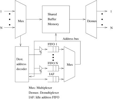
Alternatively, the logical queues can be organized with dedicated FIFO queues, one for each output port w10x. The switch architecture is shown in Figure 4.7. The performance is the same as using linked lists. The necessary amount of buffering is higher due to the buffering required for the FIFO queues, but the implementation is simpler and the multicasting and priority control easier to implement. For instance, when an incoming cell is broadcast to all output ports, it requires at least N pointer updates in Figure 4.2, while in Figure 4.7 the new address of the incoming cell can be written to all FIFO queues at the same time. The size of each FIFO in Figure 4.7 is M log M, while the size of each pointer register in Figure 4.2 is only log M, where M is the number of cells that can be stored in the shared memory. This approach
Fig. 4.7 Using FIFOs to maintain the logical queues.

CONTENT-ADDRESSABLE MEMORY APPROACH |
91 |
provides better reliability than the linked-list approach ŽFig. 4.2. in that if the cell address stored in FIFO is corrupted due to hardware failure, only one cell is affected. However, in the linked-list approach, if the pointer in the linked list is corrupted, cells in the remaining list will be either routed to an incorrect output port, or never be accessed.
4.2 CONTENT-ADDRESSABLE MEMORY APPROACH
In the CAM-based switch w14x, the shared-buffer RAM is replaced by a CAM RAM structure, where the RAM stores the cell and the CAM stores a tag used to reference the cell. This approach eliminates the need of maintaining the logical queues. A cell can be uniquely identified by its output port number and a sequence number, and these together constitute the tag. A cell is read by searching for the desired tag. Figure 4.8 shows the switch architecture. Write circuits serve input ports and read circuits serve output ports, both on a round-robin basis, as follows.
For a write:
1.Read the write sequence number WSwix from the write sequence RAM ŽWSRAM. Žcorresponding to the destination port i., and use this value Žs. for the cell’s tag {i, s}.
Fig. 4.8 Basic architecture of a CAM-based shared-memory switch.

92SHARED-MEMORY SWITCHES
2.Search the tag CAM for the first empty location, emp.
3.Write the cell into the buffer Bwempx s cell, and {i, s} into the associated tag.
4. Increment the sequence number s by one, and update WSwix with s q 1.
For a read:
1.Read the read sequence number RSw jx from the read sequence RAM ŽRSRAM. Žcorresponding to the destination port j., say t.
2.Search for the tag with the value { j, t }.
3.Read the cell in the buffer associated with the tag with the value { j, t }.
4.Increment the sequence number t by one and and update RSwix with t q 1.
This technique replaces link storage indirectly with content-addressable tag storage, and readrwrite pointersrregisters with sequence numbers. A single extra ‘‘ validity’’ bit to identify if the buffer is empty is added to each tag, effectively replacing the IAF Žand its pointers.. No address decoder is required in the CAM RAM buffer. Moreover, since the CAM does not output the address of tag matches Žhits., it requires no address encoder Žusually a source of CAM area overhead.. Both linked-list address registers and CAM-access sequence number registers must be initialized to known values on power-up. If it is necessary to monitor the length of each queue, additional counters are required for the linked-list case, while sequence numbers can simply be subtracted in the CAM-access case. Table 4.1 summa-
TABLE 4.1 Comparison of Linked List and CAM Access a
Bits |
Linked List |
CAM Access |
Cell storage |
RAM |
CAMrRAM |
Ždecoderencode. |
Ždecode. |
Žneither. |
|
256 424 s 108,544 |
256 424 s 108,544 |
lookup |
Link: RAM |
Tag:CAM |
|
256 8 s 2048 |
256 Ž4 q 7. s 2816 |
Write and read reference |
Address registers |
Sequence number registers |
Žqueue length checking. |
Žadditional counters. |
Žcompare W and R numbers. |
|
2 16 8 s 256 |
2 16 7 s 224 |
Idle address storage |
IAF |
CAM valid bit |
Žadditional overhead. |
Žpointer maintenance, |
Žnone. |
|
extra memory block. |
|
|
256 8 s 2048 |
256 1 s 256 |
|
|
|
Total |
112,896 |
111,840 |
|
|
|
aSample switch size is 16 16 with 28 s 256-cell buffer capacity; 7-bit sequence numbers are used.

SPACE TIME SPACE APPROACH |
93 |
rizes this comparison, and provides bit counts for an example single-chip configuration. Although the number of bits in the linked-list and CAM-access approaches are comparable, the latter is less attractive, due to the lower speed and higher implementation cost for the CAM chip.
4.3 SPACE–TIME–SPACE APPROACH
Figure 4.9 depicts an 8 8 example to show the basic configuration of the space time space ŽSTS. shared-memory switch w12x. Separate buffer memories are shared among all input and output ports via crosspoint space-division switches. The multiplexing and demultiplexing stages in the traditional shared-memory switch are replaced with crosspoint space switches; thus the resulting structure is referred to as STS-type. Since there is no time-division multiplexing, the required memory access speed may be drastically reduced.
The WRITE process is as follows. The destination of each incoming cell is inspected in a header detector, and is forwarded to the control block that controls the input-side space switch and thus the connection between the
Fig. 4.9 Basic configuration of STS-type shared-memory ATM switch.

94 SHARED-MEMORY SWITCHES
Fig. 4.10 Blocking in STS-type shared-memory switch.
input ports and the buffer memories. As the number of shared-buffer memories ŽSBMs. is equal to or greater than the number of input ports, each incoming cell can surely be written into an SBM as long as no SBM is full. In order to realize the buffer sharing effectively, cells are written to the least-occupied SBM first and the most-occupied SBM last. When a cell is written into an SBM, its position Žthe SBM number and the address of the cell in the SBM. is queued in the address queue. The read address selector picks out the first address from each address queue and controls the output-side space switch to connect the picked cells ŽSBMs. with the corresponding output ports.
It may occur that two or more cells picked for different output ports are from the same SBM. An example is shown in Figure 4.10. Thus, to increase the switch’s throughput it requires some kind of internal speedup to allow more than one cell to be read out from an SBM in every cell slot. Another disadvantage of this switch is the requirement of searching for the leastoccupied SBM Žmay need multiple searches in a time slot., which may cause a system bottleneck when the number of SBMs is large.
4.4 MULTISTAGE SHARED-MEMORY SWITCHES
Several proposed switch architectures interconnect small-scale shared-mem- ory switch modules with a multistage network to build a large-scale switch. Among them are Washington University gigabit switch w16x, concentratorbased growable switch architecture w4x, multinet switch w8x, Siemens switch w5x, and Alcatel switch w2x.

MULTISTAGE SHARED-MEMORY SWITCHES |
95 |
Fig. 4.11 Washington University gigabit switch. Ž 1997 IEEE..
4.4.1 Washington University Gigabit Switch
Turner proposed an ATM switch architecture called the Washington University gigabit switch ŽWUGS. w16x. The overall architecture is shown in Figure 4.11. It consists of three main components: the input port processors ŽIPPs., the output port processors ŽOPPs., and the central switching network. The IPP receives cells from the incoming links, buffers them while awaiting transmission through the central switching network, and performs the virtual-path circuit translation required to route cells to their proper outputs. The OPP resequences cells received from the switching network and queues them while they await transmission on the outgoing link. This resequencing operation increases the delay and implementation complexity. Each OPP is connected to its corresponding IPP, providing the ability to recycle cells belonging to multicast connections. The central switching network is made up of switching elements ŽSEs. with eight inputs and eight outputs and a common buffer to resolve local contention. The SEs switch cells to the proper output using information contained in the cell header, or distribute cells dynamically to provide load balancing. Adjacent switch elements employ a simple hardware flow control mechanism to regulate the flow of cells between successive stages, eliminating the possibility of cell loss within the switching network.
The switching network uses a Benes network topology.The Benes network extends to arbitrarily large configurations by way of a recursive expansion. Figure 4.11 shows a 64-port Benes network. A 512-port network can be constructed by taking 8 copies of the 64-port network and adding the first and fifth stage on either side, with 64 switch elements a copy. Output j of the ith switch element in the first stage is then connected to input i of the jth 64-port network. Similarly, output j of the ith 64-port network is connected