

Design Techniques for EMC – Part 4
Shielding
By Eur Ing Keith Armstrong CEng MIEE MIEEE
Partner, Cherry Clough Consultants, Associate of EMC-UK
This is the fourth in a series of six articles on best-practice EMC techniques in electrical/electronic/mechanical hardware design. The series is intended for the designer of electronic products, from building block units such as power supplies, single-board computers, and “industrial components” such as motor drives, through to stand-alone or networked products such computers, audio/video/TV, instruments, etc.
The techniques covered in the six articles are:
1)Circuit design (digital, analogue, switch-mode, communications), and choosing components
2)Cables and connectors
3)Filters and transient suppressors
4)Shielding
5)PCB layout (including transmission lines)
6)ESD, electromechanical devices, and power factor correction
A textbook could be written about any one of the above topics (and many have), so this magazine article format can only introduce the various issues and point to the most important best-practice techniques. Many of the techniques described in this series are also important for improving signal integrity: reducing the number of iterations during development and reducing manufacturing costs.
Table of contents for this part
4.Shielding
4.1Shielding and the commercial imperative
4.2General concepts in shielding
4.3Bigger and rectangular is better
4.4Skin effect
4.5Apertures
4.6Low frequency (magnetic field) shielding
4.7Waveguides below cutoff
4.8Gasketting
4.9Shielding of displays (and the like)
4.10Shielding ventilation apertures
4.11Shielding with painted or plated plastics
4.12Shielding without metal
4.13Failing conducted tests due to inadequate shielding
4.14Installation of shielded enclosures
4.15Using PCB-level shielding
4.16Further reading
Design techniques for EMC – Part 4 – Shielding |
Cherry Clough Consultants |
Page 1 of 23 |
4.Shielding
4.1Shielding and the commercial imperative
A complete volumetric shield is often known as a "Faraday Cage", although this can give the impression that a cage full of holes (like Mr Faraday’s original) is acceptable, which it generally isn’t.
There is a cost hierarchy to shielding which makes it commercially very important to consider shielding early in the design process. Shields may be fitted around:
• |
Individual ICs |
example cost 25p |
• Segregated areas of PCB circuitry |
example cost £1 |
|
• |
Whole PCBs |
example cost £10 |
• |
Sub-assemblies and modules |
example cost £15 |
• |
Complete products |
example cost £100 |
• Assemblies (e.g. industrial control and instrumentation cubicles) |
example cost £1,000 |
|
• |
Rooms |
example cost £10,000 |
• |
Buildings |
example cost £100,000 |
Please don’t take these example costs as more than a very rough guide to orders of magnitude for domestic, commercial and industrial products. For example the shielding used in the new MI6 building in London will have cost very much more than £100,000, and that used on a flight-critical avionics computer will cost a lot more than £100. These costs do not take account of the reengineering costs of adding shielding late in a project, which can be very much greater. They also don’t take account of the lost sales and market position which can result from delays caused by shield re-engineering late in a project.
The important point is that shielding can be very low cost if it is designed-in carefully from the start, but can be extremely expensive indeed if it has to be applied at the last minute to make a product acceptable to a customer (or to an EMC enforcement agent).
Shielding always adds cost and weight, so it is always best to use the other techniques described in this series to improve EMC and reduce the need for shielding. Even where it is hoped to avoid shielding altogether it is best to allow for Murphy’s Law and design from the start so that shielding can be added later if necessary. Mr Murphy can usually be discouraged from upsetting your product roll-out if you have a variety of shielding (and filtering) solutions ready to be dropped in when you first test your new product for EMC.
A degree of shielding can also be achieved by keeping all conductors and components very close to a solid metal sheet. Ground-planed PCBs populated entirely by low-profile surface mounted devices are therefore recommended for their EMC advantages. Even though such PCBs may require additional enclosure (volumetric) shielding, it should not need to have as high a shielding effectiveness (SE) and so will be easier to make and cost less.
A useful degree of shielding can be achieved in electronic assemblies by keeping their internal electronic units and cables very close to an earthed metal surface at all times, and bonding their earths directly to it instead of (or as well as) using a safety star earthing system based on green/yellow wires. This technique usually uses zinc-plated mounting plates or chassis, and can help avoid the need for high values of enclosure SE.
4.2General concepts in shielding
Many textbooks have been written on the subject of how shields work, and it is not intended to repeat them here. However, a few broad concepts will help. A shield puts an impedance discontinuity in the path of a propagating radiated electromagnetic wave, reflecting it and/or absorbing it. This is conceptually very similar to the way in which filters work – they put an
Design techniques for EMC – Part 4 – Shielding |
Cherry Clough Consultants |
Page 2 of 23 |
impedance discontinuity in the path of an unwanted conducted signal. The greater the impedance ratio, the greater the SE.
At thicknesses of 0.5mm or over, most normal fabrication metals provide good SE above 1MHz and excellent SE above 100MHz. Problems with metal shields are mostly caused by thin materials, frequencies below 1MHz, and apertures, and this article focuses mainly on these.
4.3Bigger and rectangular is better
It is generally best to allow a large distance between the circuits being shielded and the walls of their shield. The emitted fields outside the shield, and the fields that the devices are subjected to, will generally be more “diluted” the larger the shielded volume. This advice generally raises hollow laughter, since most product design seems to be about fitting a quart into a pint pot.
Where enclosures have parallel walls opposite each other standing waves can build up at resonant frequencies, and these can cause SE problems. Irregular shaped enclosures, or ones with curved or non-parallel walls (more hollow laughter) will help prevent resonances. Where opposing shield walls are parallel, try to prevent the resonances due to the width, height, or length from occurring at the same frequencies. So avoid cubic enclosures, use rectangular cross-sections instead of square, and try to avoid dimensions that are simple multiples of each other. E.g. if the length is 1.5 times the width, the second resonance of the width coincides with the third resonance of the length. Best to use irrationally ratio’d dimensions, such as that provided by the venerable Fibonacci series (which the Greeks knew as the Golden Mean). It is probably not worth worrying too much about this because the internal PCBs, components, and wiring alter its resonances unpredictably anyway.
4.4Skin effect
Fields come in two flavours: electric (E) and magnetic (M). Electromagnetic fields consist of E and M fields in a given ratio (giving a wave impedance E/M of 377Ω in air). Electric fields are easily stopped by thin metal foils, since the mechanism for electric field shielding is one of charge redistribution at a conductive boundary, so almost anything with a high conductivity (low resistance) will present a suitably low impedance. At high frequencies quite considerable displacement currents can result from the rapid rate of charge re-distribution, but even thin aluminium can cope with this quite nicely.
However, magnetic fields are much more difficult to stop. They need to generate eddy currents inside the shield material to create magnetic fields that oppose the impinging field. Thin aluminium is not going to be very suitable for this purpose, and the depth of current penetration required for a given SE depends on the frequency of the field, and on the characteristics of the metal used for the shield, and is known as the “skin effect”.
One skin depth is the depth in the shield material at which the “skin effect” causes the currents caused by the impinging magnetic field to be reduced by approximately 9dB. So a material which was as thick as 3 skin depths would have an approximately 27dB lower current on its opposite side and have an SE of approximately 27dB for that M field.
Skin effect is especially important at low frequencies, where the fields experienced are more likely to be predominantly magnetic with a lower wave impedance than 377Ω. The formula for skin depth is given in most textbooks, but requires knowledge of the shielding material’s conductivity and relative permeability. Figure 4A solves this for aluminium and steel, with copper thrown in for comparison. Pure zinc will have skin depths close to those of aluminium.
Design techniques for EMC – Part 4 – Shielding |
Cherry Clough Consultants |
Page 3 of 23 |
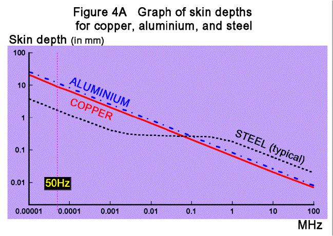
Copper and aluminium have over 5 times the conductivity of steel, so are very good at stopping electric fields, but have a relative permeability of 1 (the same as air). Typical mild steel has a relative permeability of around 300 at low frequencies, falling to 1 as frequencies increase above 100kHz, and its higher permeability gives it a reduced skin depth, making reasonable thicknesses of mild steel better than aluminium for shielding low frequencies. Different grades of steels (especially stainless) have different conductivities and permeabilities, and their skin depths will vary considerably as a result.
A good material for a shield will have high conductivity and high permeability, and sufficient thickness to achieve the required number of skin-depths at the lowest frequency of concern. 1mm thick mild steel plated with pure zinc (say, 10 microns or more) is just fine for many applications.
4.5Apertures
It is easy to achieve SE figures of 100dB or more at frequencies above 30MHz with ordinary constructional metalwork. But this assumes a perfectly enclosing shield volume with no joints or gaps, which makes assembly of the product rather difficult unless you are prepared to seam-weld it all around and also have no external cables, antennae, or sensors (rather an unusual product).
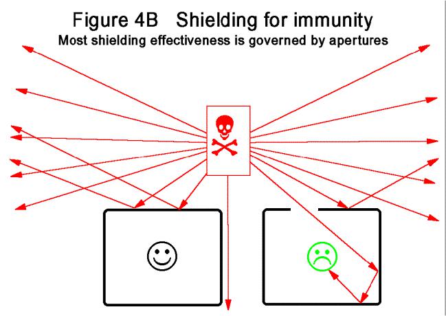
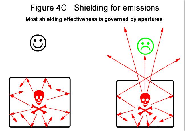
In practice, whether shielding is being done to reduce emissions or improve immunity, most shield performance is limited by the apertures in it, as these two simple figures 4B and 4C try to show.
Design techniques for EMC – Part 4 – Shielding |
Cherry Clough Consultants |
Page 4 of 23 |
Design techniques for EMC – Part 4 – Shielding |
Cherry Clough Consultants |
Page 5 of 23 |
Considering apertures as holes in an otherwise perfect shield implies that they act as half-wave resonant “slot antennae”, and this allows us to make predictions about maximum aperture sizes for a given SE: for a single aperture, SE = 20log(λ/2d) where λ is the wavelength at the frequency of interest and d is the longest dimension of the aperture. In practice this assumption may not always be accurate, but it has the virtue of being an easy design tool that is better than doing nothing. Where its predications found to be are inaccurate it may be possible to refine it following practical experiences with the technologies and construction methods used on specific products.
The resonant frequency of a slot antenna is governed by its longest dimension – its diagonal. It makes little difference how wide or narrow an aperture is, or even whether there is a line-of-sight through the aperture.
Even apertures the thickness of a paint or oxide film, formed by overlapping metal sheets, still radiate (leak) at their resonant frequency as well as if they were wide enough to poke a finger through.
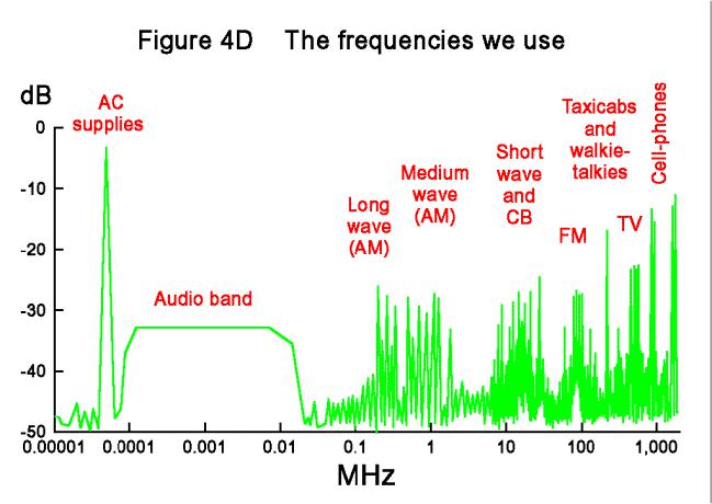
Figures 4D and 4E have been used before in this series to try to give a feel for the fact that the frequencies inside modern electronic products use the same range of frequencies as we rely on for communications and broadcasting.
Design techniques for EMC – Part 4 – Shielding |
Cherry Clough Consultants |
Page 6 of 23 |
Design techniques for EMC – Part 4 – Shielding |
Cherry Clough Consultants |
Page 7 of 23 |

One of the most important EMC issues is keeping the products’ internal frequencies inside, so they don’t pollute the radio spectrum outside.
Figure 4F shows how effective apertures in shields can be at behaving like antennas and allowing the internal frequencies to disturb the radio spectrum and cause interference.
Design techniques for EMC – Part 4 – Shielding |
Cherry Clough Consultants |
Page 8 of 23 |
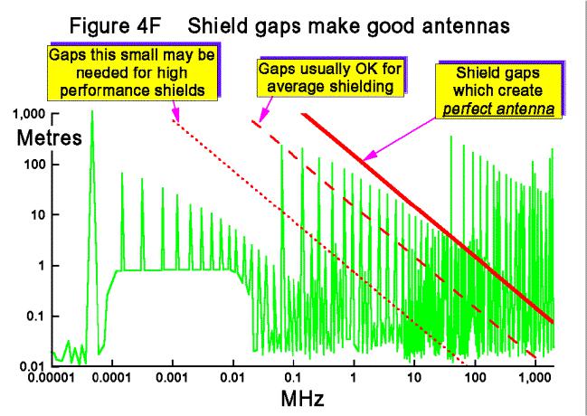
The half-wave resonance of slot antennae (expressed in the above rule of thumb: SE = 20log(λ/2d)) is the basis for the solid line in figure 4F (and for the rule-of-thumb of figure 4G) using the relationship ν = fλ (where ν is the speed of light: 3.108 metres/sec, f is the frequency in Hz, and λ
is the wavelength in metres).
We find that a narrow 430mm long gap along the front edge of a 19-inch rack unit’s front panel will be half-wave resonant at around 350MHz. At this frequency our example 19” front panel is no longer providing much shielding, and removing it entirely might not make much difference.
Figure 4G is useful when estimating the maximum size of an aperture for a given SE, and may be easily scaled to suit different dimensions.
Design techniques for EMC – Part 4 – Shielding |
Cherry Clough Consultants |
Page 9 of 23 |
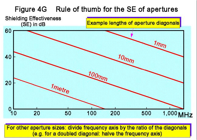
For an SE of 20dB at 1GHz (the present upper limit of testing in most standards) figure 4G suggests an aperture no larger than around 16 mm. For 40dB this would be only 1.6 mm, requiring gaskets to seal apertures and/or the use of the waveguide below cutoff techniques described later.
Actual SE in practice will depend on internal resonances between the walls of the enclosure itself, the proximity of components and conductors to apertures (keep noisy cables such as ribbon cables carrying digital busses well away from shield apertures and joints), the impedances of the fixings used to assemble the parts of the enclosure, etc.
Wherever possible, break all necessary or unavoidable apertures into a number of smaller ones. Unavoidably long apertures (covers, doors, etc) may need conductive gaskets or spring fingers (or other means of maintaining shield continuity). The SE of a number of small identical apertures nearby each other is (roughly) proportional to their number (∆SE = 20logn, where n is the number of apertures), so two apertures will be worse by 6dB, four by 12dB, 8 by 18dB, and so on. But when the wavelength at the frequency of concern starts to become comparable with the overall size of the array of small apertures, or when apertures are not near to each other (compared with the wavelength), this crude ‘6dB per doubling’ rule breaks down because of phase cancellation effects. However, at least this simple rule errs on the side of caution.
Apertures placed more than half a wavelength apart do not in general worsen the SEs that each achieves individually, but half a wavelength at 100MHz is 1.5 metres, so at such low frequencies on typical products smaller than this an increased number of apertures will tend to worsen the enclosure’s SE.
Apertures don’t merely behave as slot antennae. Currents flowing in a shield and forced to divert their path around an aperture will cause it to emit magnetic fields. Voltage differences across an aperture will cause the aperture to emit electric fields. The author has seen dramatic levels of
Design techniques for EMC – Part 4 – Shielding |
Cherry Clough Consultants |
Page 10 of 23 |