

05.Implementation technologies
.pdfChapter 5 − Implementation Technologies |
Page 21 of 27 |
w x y z
F1
F2
F3
♦
5.9Complex Programmable Logic Device (CPLD)
Using ROMs, PLAs, and PALs to implement a combinational circuit is fairly straight forward and easy to do. However, to implement a sequential circuit or a more complex combinational circuit may require more sophisticated and larger programming devices. The complex programmable logic device (CPLD) is capable of implementing a circuit with upwards of 10,000 logic gates.
The CPLD contains many PAL-like blocks connected together using a programmable interconnect to form a matrix. The PAL-like blocks in the CPLD are called macrocells as shown in Figure 21. Each macrocell has a programmable-AND-fixed-OR array similar to a PAL device for implementing combinational logic operations. The XOR gate in the macrocell circuit shown in Figure 21 will either invert or not invert the output from the combinational logic. Furthermore, a flip-flop is included to provide the capability of implementing sequential logic operations. The flip-flop can be bypassed for combinational logic operations.
Groups of 16 macrocells are connected together to form the logic array blocks. Multiple logic array blocks are linked together using the programmable interconnect array as shown in Figure 22. Logic signals are routed between the logic array blocks on the programmable interconnect array. This global bus is a programmable path that connects any signal source to any destination on the CPLD.
The I/O control block allows each I/O pin to be individually configured for input, output, or bi-directional operation. All I/O pins have a tri-state buffer that is individually controlled. The I/O pin is configured as an input port if the tri-state buffer is disabled, otherwise, it is an output port.
Figure 23 shows some of the main features of the Altera MAX 7000 CPLD. Instead of needing a separate programmer to program the CPLD, all MAX devices support in-system programmability through the IEEE JTAG interface. This allows designers to program the CPLD after it is mounted on a printed circuit board. Furthermore, the device can be reprogrammed in the field. CPLDs are non-volatile, so once they are programmed with a circuit, the circuit remains implemented in the device even when power is removed.
Microprocessor Design – Principles and Practices with VHDL |
Last updated 7/16/2003 12:29 PM |

Chapter 5 − Implementation Technologies |
Page 22 of 27 |
D |
Q |
Clk |
|
D |
Q |
Clk |
|
Figure 21. Circuit for the logic array block with two macrocells.
|
|
|
|
|
|
|
|
|
|
I/O |
|
|
|
|
|
|
I/O |
||||
|
|
|
|
|
|
|
|
|
Block |
|
|
|
|
|
Block |
||||||
|
|
|
|
|
|
|
|
|
|
|
|
|
|
|
|
|
|
|
|
|
|
|
|
|
|
|
|
|
|
|
|
|
|
|
|
|
|
|
|
|
|
|
|
|
|
|
|
|
|
|
|
|
|
|
|
|
|
|
|
|
|
|
|
|
|
|
|
|
|
|
|
|
|
|
|
|
|
|
|
|
|
|
|
|
|||
I/O |
|
|
|
|
|
|
|
|
|
|
|
|
|
|
|
|
|
|
|
||
|
|
|
|
Programmable Interconnect |
|
|
|
|
|||||||||||||
Block |
|
|
|
|
|
|
|
|
|
|
|
||||||||||
|
|
|
|
|
|
|
|
|
|
|
|
|
|
|
|
|
|
|
|||
|
|
|
|
|
|
|
|
|
|
|
|
|
|
|
|
|
|
|
|
|
|
|
|
|
|
|
|
|
|
|
|
|
|
|
|
|
|
|
|
|
|
|
|
|
|
|
|
|
Logic |
|
|
Programmable |
|
|
Logic |
|
|
Programmable |
|
||||||
|
|
|
|
|
Array |
|
|
|
|
Array |
|
|
|
||||||||
|
|
|
|
|
|
|
|
|
|
|
|
|
|
|
|
||||||
|
|
|
|
|
Block |
|
|
|
|
|
|
Block |
|
|
|
|
|
||||
|
|
|
|
|
|
|
|
|
|
|
|
|
|
|
|
|
|
|
|
|
|
|
|
|
|
|
|
|
|
|
|
|
|
|
|
|
|
|
|
|
|
|
|
I/O |
|
|
|
|
|
|
|
|
|
|
|
|
|
|
|
|
|
|
|
|
|
|
|
|
|
|
|
Interconnect |
|
|
|
|
|
Interconnect |
|||||||||
Block |
|
|
|
|
Logic |
|
|
Logic |
|
||||||||||||
|
|
|
|
|
|
|
|
|
|
|
|
|
|
|
|
|
|
|
|
|
|
|
|
|
|
|
|
|
|
|
|
|
|
|
|
|
|
|
|
|
|
|
|
|
|
|
|
|
|
|
|
|
|
|
|
|
|
|
|
|
|
|
|
|
|
|
|
|
|
|
Array |
|
|
|
|
|
|
Array |
|
|
|
|
|
||||
|
|
|
|
|
Block |
|
|
|
|
|
|
Block |
|
|
|
|
|
||||
|
|
|
|
|
|
|
|
|
|
|
|
|
|
|
|
|
|
|
|
|
|
|
|
|
|
|
|
|
|
|
|
|
|
|
|
|
|
|
|
|
|
|
|
|
|
|
|
|
|
|
|
|
|
|
|
|
|
|
|
|
|
|
|
|
|
|
|
|
|
|
|
|
|
|
|
|
|
|
|
|
|
|
|
|
|
|
|
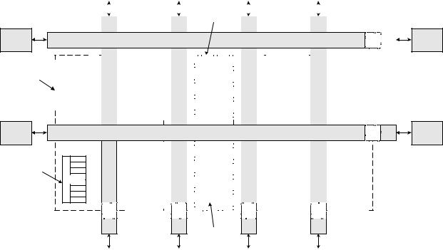
I/O |
|
I/O |
Block |
|
Block |
Figure 22. Internal circuit for a complex programmable logic device (CPLD).
Microprocessor Design – Principles and Practices with VHDL
I/O
Block
I/O
Block
Last updated 7/16/2003 12:29 PM
Chapter 5 − Implementation Technologies |
|
Page 23 of 27 |
|
|
|
|
|
Feature |
|
MAX7000 CPLD |
FLEX10K FPGA |
Usable logic gates |
|
10,000 |
250,000 |
Macrocells |
|
512 |
N/A |
Logic array blocks |
|
32 |
1,520 |
User I/O pins |
|
212 |
470 |
Figure 23. Features of the Altera MAX 7000 CPLD and the FLEX10K250 FPGA.
5.10 Field-Programmable Gate Array (FPGA)
Field-programmable gate arrays (FPGAs) are complex programmable logic devices that are capable of implementing up to 250,000 logic gates and up to 40,960 RAM bits as featured by the Altera FLEX10K250 FPGA chip. See Figure 23. The internal circuitry of the FLEX10K FPGA is shown in Figure 24. The device contains an embedded array and a logic array. The embedded array is used to implement memory functions and complex logic functions such as microcontroller and digital signal processing. The logic array is used to implement general logic such as counters, arithmetic logic units, and state machines.
I/O
Block
|
|
|
|
LE |
||
|
|
|||||
Logic Array |
|
|
|
LE |
||
|
|
|
|
|
|
|
|
|
|
|
LAB |
|
|
|
|
|
|
|
|
|
|
|
|
|
|
|
|
|
|
|
|
|
|
|
|
|
|
|
|
|
|
|
|
|
|
|
|
|
I/O
Block
Logic Array
Block
LAB
|
|
I/O |
|
|
|
|
|
|
|
|
|
|
|
|
|
|
|
I/O |
|
|
|
|
|
|
I/O |
|
|
|
|
|
|
|
|
|
|
|
|
|
I/O |
|
|
|
|
|
|
|
||||||||||||||||||||||
|
Block |
|
|
|
|
|
|
|
|
|
|
|
|
|
|
Block |
|
|
|
|
|
Block |
|
|
|
|
|
|
|
|
|
|
|
|
Block |
|
|
|
|
|
|
|
||||||||||||||||||||||||||
|
|
|
|
|
|
|
|
|
|
|
|
|
|
|
|
|
|
|
|
|
|
|
Embedded |
|
|
|
|
|
|
|
|
|
|
|
|
|
|
|
|
|
|
|
|
|
|
|
|
|
|
|
|
|
|
|
|
|
|
|
|
|||||||||
|
|
|
|
|
|
|
|
|
|
|
|
|
|
|
|
|
|
|
|
|
|
|
|
|
|
|
|
|
|
|
|
|
|
|
|
|
|
|
|
|
|
|
|
|
|
|
|
|
|
|
|
|
|
|
|
|||||||||||||
|
|
|
|
|
|
|
|
|
|
|
|
|
|
|
|
|
|
|
|
|
|
|
|
Array |
|
|
|
|
|
|
|
|
|
|
|
|
|
|
|
|
|
|
|
|
|
|
|
|
|
|
|
|
|
|
|
|
|
|
|
|
|
|
||||||
|
|
|
|
|
|
|
|
|
|
|
|
|
|
|
|
|
|
|
|
|
|
|
|
|
|
|
|
|
|
|
|
|
|
|
|
|
|
|
|
|
|
|
|
|
|
|
|
|
|
|
|
|
|
|
|
|
|
|
|
|
|
|
||||||
|
|
|
|
|
|
|
|
|
|
|
|
|
|
|
|
|
|
|
|
|
|
|
|
|
|
|
|
|
|
|
|
|
|
|
|
|
|
|
|
|
|
|
|
|
|
|
|
|
|
|
|
|
|
|
|
|
|
|
|
|
|
|
||||||
|
|
|
|
|
|
|
Row Interconnect |
|
|
|
|
|
|
|
|
|
|
|
|
|
|
|
|
|
|
|
|
|
|
|
|
|
|
|
|
|
|
|
|
|
|
|
|
|
|
|
|
|
|
|
|
|
|
|||||||||||||||
|
|
Column |
|
|
|
|
|
|
|
|
|
|
|
|
|
|
|
|
Column |
|
|
|
|
|
|
|
|
|
|
|
|
|
|
|
|
|
|
|
|
|
|
|
|
|
|
|
|
|
|
|
|
|
|
|
|
|
|
|
|
|
|
|
|
|
|
|
||
|
|
|
|
|
|
|
|
|
|
|
|
|
|
|
|
|
|
|
|
|
|
|
|
|
|
|
|
|
|
|
|
|
|
|
|
|
|
|
|
|
|
|
|
|
|
|
|
|
|
|
|
|
|
|
|
|
|
|
|
|
|
|||||||
|
|
|
|
|
|
|
|
|
|
|
|
|
|
|
|
|
|
|
|
|
|
|
|
|
|
|
|
|
|
|
|
|
|
|
|
|
|
|
|
|
|
|
|
|
|
|
|
|
|
|
|
|
|
|
|
|
|
|
|
|
|
|||||||
|
|
|
|
|
|
|
|
|
|
|
|
|
|
|
|
|
|
|
|
|
|
|
|
|
|
|
|
|
|
|
|
|
|
|
|
|
|
|
|
|
|
|
|
|
|
|
|
|
|
|
|
|
|
|
|
|
|
|
|
|
|
|
|
|
||||
|
|
Interconnect |
|
|
|
|
|
|
|
LAB |
|
|
|
|
|
|
Interconnect |
|
|
EAB |
|
|
|
|
|
|
|
|
|
|
|
LAB |
|
|
|
|
|
|
|
|
|
|
|
|
|
|
|
|
|
LAB |
|
|
|
|
|
|
|
|||||||||||
|
|
|
|
|
|
|
|
|
|
|
|
|
|
|
|
|
|
|
|
|
|
|
|
|
|
|
|
|
|
|
|
|
|
|
|
|
|
|
|
|
|
|
|
|
|
|
|
|
|
|
|
|
|
|
|
|
|
|
|
|
|
|
|
|
|
|
|
|
|
|
|
|
|
|
|
|
|
|
|
|
|
|
|
|
|
|
|
|
|
|
|
|
|
|
|
|
|
|
|
|
|
|
|
|
|
|
|
|
|
|
|
|
|
|
|
|
|
|
|
|
|
|
|
|
|
|
|
|
|
|
|
|
|
|
|
|
|
|
|
|
|
|
|
|
|
|
|
|
|
|
|
|
|
|
|
|
|
|
|
|
|
|
|
|
|
|
|
|
|
|
|
|
|
|
|
|
|
|
|
|
|
|
|
|
|
|
|
|
|
|
|
|
|
|
|
|
|
|
|
|
|
|
|
|
|
|
|
|
|
|
|
|
|
|
|
|
|
|
|
|
|
|
|
|
|
|
|
|
|
|
|
|
|
|
|
|
|
|
|
|
|
|
|
|
|
|
|
|
|
|
|
|
|
|
|
|
|
|
|
|
|
|
|
|
|
|
|
|
|
|
|
|
|
|
|
|
|
|
|
|
|
|
|
|
|
|
|
|
|
|
|
|
|
|
|
|
|
|
|
|
|
|
|
|
|
|
|
|
|
|
|
|
|
|
|
|
|
|
|
|
|
|
|
|
|
|
|
|
|
|
|
|
|
|
|
|
|
|
|
|
|
|
|
|
Row Interconnect
|
|
|
|
|
|
|
|
|
|
|
|
|
|
|
|
|
|
|
|
|
|
|
|
|
|
|
|
|
|
|
|
|
|
|
|
|
|
|
|
|
|
|
|
|
|
|
|
|
|
|
|
|
|
|
|
|
|
|
|
|
|
|
|
|
|
|
|
|
|
|
|
|
|
|
|
|
|
|
|
|
|
|
|
|
|
|
|
|
|
|
|
|
|
|
|
|
|
|
|
|
|
|
|
|
|
|
|
|
|
|
|
|
|
|
|
|
|
|
|
|
|
|
|
|
|
|
|
|
|
|
|
|
|
|
|
|
|
|
|
|
|
|
|
|
|
|
|
|
|
|
|
|
|
|
|
|
|
|
|
|
|
|
|
|
|
|
|
|
|
|
|
|
|
|
|
|
|
|
|
|
|
|
|
|
|
|
|
|
|
|
|
|
|
|
|
|
|
|
|
|
|
|
|
|
|
|
|
|
|
|
|
|
|
|
|
|
|
|
|
|
|
|
|
|
|
|
|
|
|
|
|
|
|
|
|
|
|
|
|
|
|
|
|
|
|
|
|
|
|
|
|
|
|
|
|
|
|
LAB |
|
|
|
|
|
|
|
|
|
|
EAB |
|
|
|
|
|
|
|
|
|
LAB |
|
|
|
|
|
|
|
|
|
|
|
|
|
LAB |
|
|
||||||||||
|
|
|
|
|
|
|
|
|
|
|
|
|
|
|
|
|
|
|
|
|
|
|
|
|
|
|
|
|
|
|
|
|
|
|
|
|
||||||||||||||
|
|
|
|
|
|
|
|
|
|
|
|
|
|
|
|
|
|
|
|
|
|
|
|
|
|
|
|
|
|
|
|
|
|
|
|
|
|
|
|
|
|
|
|
|
|
|
|
|
|
|
|
|
|
|
|
|
|
|
|
|
|
|
|
|
|
|
|
|
|
|
|
|
|
|
|
|
|
|
|
|
|
|
|
|
|
|
|
|
|
|
|
|
|
|
|
|
|
|
|
|
|
|
|
|
|
|
|
|
|
|
|
|
|
|
|
|
|
|
|
|
|
|
|
|
|
|
|
|
|
|
|
|
|
|
|
|
|
|
|
|
|
|
|
|
|
|
|
|
|
|
|
|
I/O
Block
I/O
Block
Embedded
Array Block
I/O |
|
I/O |
|
I/O |
|
I/O |
Block |
|
Block |
|
Block |
|
Block |
Figure 24. FLEX 10K FPGA circuit.
The embedded array consists of a series of embedded array blocks (EABs). When implementing memory functions, each EAB provides 2,048 bits, which can be used to create RAM, dual-port RAM, or ROM. EABs can be used independently, or multiple EABs can be combined to implement larger functions.
The logic array consists of logic array blocks (LABs). Each LAB contains eight logic elements (LE) and a local interconnect. The LE shown in Figure 25 is the smallest logical unit in the FLEX 10K architecture. Each LE consists of a 4-input look-up table (LUT) and a programmable flip-flop. The 4-input LUT is a function generator made from a 16-to-1 multiplexer that can quickly compute any function of four variables. Refer to section 4.8 on how multiplexers are used to implement Boolean functions. The four input variables are connected to the four select lines
Microprocessor Design – Principles and Practices with VHDL |
Last updated 7/16/2003 12:29 PM |

Chapter 5 − Implementation Technologies |
Page 24 of 27 |
of the multiplexer. Depending on the values of these four variables, the value from one of the 16 multiplexer inputs is passed to the output. There are 16 1-bit registers connected to the 16 multiplexer inputs to supply the multiplexer input values. Depending on the function to be implemented, the content of the 1-bit registers is set to a 0 or a 1. It is set to a 1 for all the 1-minterms of the four variable function, and to a 0 for all the 0-minterms. The LUT in the figure implements the four variable function F(w,x,y,z) = Σ (0, 3, 5, 6, 7, 12, 13, 15). The programmable flip-flop can be configured for D, T, JK, or SR operation, and is used for sequential circuits. For combinational circuits, the flipflop can be bypassed.
4-input LUT
1 |
0 |
1 |
1 |
0 |
0 |
0 |
0 |
1 |
1 |
1 |
0 |
1 |
0 |
0 |
1 |
variable 1 |
|
|
|
|
|
|
|
|
|
|
|
|
|
|
|
|
|
|
|
|
|
Register bypass |
|
|
|
|
|
|
||||||||
|
|
|
15 14 13 12 11 10 9 |
8 |
7 |
6 |
5 |
4 |
3 |
2 |
1 |
0 |
|
|
|
|
|
|
|
|
|
|
|
|
|
|
||||||||||
variable 2 |
|
|
|
|
|
|
16-to-1 mux |
|
|
|
|
|
|
|
|
|
|
|
|
|
|
|
|
|
|
|||||||||||
|
|
|
|
|
|
|
|
|
|
|
|
|
|
|
|
|
|
|
|
|
|
|
|
|
||||||||||||
|
|
|
|
|
|
|
|
|
|
|
|
|
|
|
|
|
|
|
|
|
|
|
|
|||||||||||||
variable 3 |
|
|
|
|
|
|
|
|
|
|
|
|
|
|
|
|
|
|
|
|
|
|
|
|
|
|||||||||||
|
|
|
|
|
|
|
|
|
|
|
|
|
|
|
|
|
|
|
|
|
|
|
|
|
|
|
|
|
|
|
|
|
|
|
|
|
variable 4 |
|
|
|
|
|
|
|
|
|
|
|
|
|
|
|
|
|
|
|
|
|
|
|
|
|
|
|
|
|
|
|
|
|
|
|
To interconnect |
|
|
|
|
|
|
|
|
|
|
|
|
|
|
|
|
|
|
|
|
|
|
|
|
|
|
|
|
|
|
|
|
|
|
|
||
|
|
|
|
|
|
|
|
|
|
|
|
|
|
|
|
|
|
|
|
|
|
|
|
|
|
|
|
|
|
|
|
|
|
|
|
|
|
|
|
|
|
|
|
|
|
|
|
|
|
|
|
|
|
|
|
|
|
|
|
|
|
|
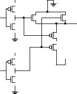
D |
Set |
Q |
|
|
|
|||||
|
|
|
|
|
|
|
|
|
|
|
|
|
|
|
|
|
|
|
|
|
|
|
|
|
|
|
|
|
|
|
|
|||||
|
|
|
|
|
|
|
|
|
|
|
|
|
|
|
|
|
|
|
|
|
|
|
Clock |
|
|
|
|
|
|
|
|
|
|
|||
|
|
|
|
|
|
|
|
|
|
|
|
|
|
|
|
|
|
|
|
|
|
|
|
|
|
|
|
|
|
|
|
|
|
|
||
|
|
|
|
|
|
|
|
|
|
|
|
|
|
|
|
|
|
|
|
|
|
|
|
|
Clear |
|
Register bypass |
|||||||||
|
|
|
|
|
|
|
|
|
|
|
|
|
|
|
|
|
|
|
|
|
|
|
|
|
|
|
|
|||||||||
|
|
|
|
|
|
|
|
|
|
|
|
|
|
|
|
|
|
|
|
|
|
|
|
|
|
|
|
|
select |
|||||||
|
|
|
|
|
|
|
|
|
|
|
|
|
|
|
|
|
|
|
|
|
|
|
|
|
|
|
|
|
|
|
|
|
|
|
|
|
Programmable
flip-flop
Figure 25. Logic element circuit with a 4-input LUT and a programmable register.
All the EABs and LABs, along with the I/O elements are connected together via the FastTrack Interconnect, which is a series of fast row and column buses that run the entire length and width of the device. The interconnect contains programmable switches so that the output of any block can be connected to the input of any other block.
Each I/O pin in an I/O element is connected to the end of each row and column of the interconnect and can be used as either an input, output, or bi-directional port.
5.11Summary Checklist
Voltage levels
weak-0, weak-1
NMOS
NMOS truth table
PMOS
PMOS truth table
High-impedance Z
Transistor circuits for basic gates
PLD
ROM circuit implementation
PLA circuit implementation
PAL circuit implementation
CPLD
FPGA
5.12References
www.altera.com
www.xilinx.com
Microprocessor Design – Principles and Practices with VHDL |
Last updated 7/16/2003 12:29 PM |
Chapter 5 − Implementation Technologies |
Page 25 of 27 |
5.13 Exercises
5.1.Draw the CMOS circuit for the AND gate by using two NMOS transistors for the 0 half of the circuit and two PMOS transistors for the 1 half of the circuit.
Answer
Vcc
A
Output
Vcc
Vcc
B
5.2. d
Microprocessor Design – Principles and Practices with VHDL |
Last updated 7/16/2003 12:29 PM |
Chapter 5 − Implementation Technologies
Index
A
Analysis
CMOS circuits, of, 12
AND
CMOS circuit, 7
C
CMOS, 2, 4 AND gate, 7 circuit, 5 inverter, 5 logic, 4 multiplexer, 10 NAND gate, 6 NOR gate, 9 OR gate, 9
Transmission gate, 9 XNOR gate, 12 XOR gate, 12
Combinational circuit
PAL implementation of, 19 PLA implementation of, 16 ROM implementation of, 13
Complementary metal oxide semiconductor. See CMOS
Complex programmable logic device, 21 CPLD. See Complex programmable logic device
E
EPROM. See Erasable programmable read-only memory
Erasable programmable read-only memory, 14
F
Field-programmable gate array, 23 FPGA. See Field-programmable gate array
H
High impedance, 4, 5
M
MOSFET, 3
Multiplexer
CMOS circuit, 10
N
NAND
CMOS circuit, 6
Page 26 of 27
n-channel, 3, 4 NMOS, 4 NOR
CMOS circuit, 9 NOT
CMOS circuit, 5
O
OR
CMOS circuit, 9
P
PAL. See Programmable array logic p-channel, 3, 4
PLA. See Programmable logic array PMOS, 4, 5
Programmable array logic, 19 Programmable logic array, 16 Programmable read-only memory, 14
PROM. See Programmable read-only memory
R
Read-only memory, 13
ROM. See read-only memory
S
Short. See Short circuit
Short circuit, 5, 6
T
Transistor technologies, 2 bipolar logic, 2
complementary metal oxide semiconductor logic (CMOS), 2
diode-transistor logic, 2 transistor-transistor logic (TTL), 2
Transmission gate, 9
W
weak 0, 2, 5 weak 1, 2, 4, 5
X
XNOR
CMOS circuit, 12
XOR
CMOS circuit, 12
Microprocessor Design – Principles and Practices with VHDL |
Last updated 7/16/2003 12:29 PM |
Chapter 5 − Implementation Technologies |
Page 27 of 27 |
Z |
Z. See High impedance |
Microprocessor Design – Principles and Practices with VHDL |
Last updated 7/16/2003 12:29 PM |