

06.Latches and flip-flops
.pdfChapter 6 – Latches and Flip-Flops Page 1 of 27
Table of Content
Table of Content ........................................................................................................................................................... |
1 |
|||
6 |
Latches and Flip-Flops.......................................................................................................................................... |
2 |
||
|
6.1 |
Bistable Element ........................................................................................................................................... |
2 |
|
|
6.2 |
SR Latch........................................................................................................................................................ |
4 |
|
|
6.3 |
SR Latch with Enable.................................................................................................................................... |
6 |
|
|
6.4 |
D Latch.......................................................................................................................................................... |
7 |
|
|
6.5 |
D Latch with Enable...................................................................................................................................... |
7 |
|
|
6.6 |
Clock ............................................................................................................................................................. |
8 |
|
|
6.7 |
D Flip-Flop.................................................................................................................................................. |
10 |
|
|
6.8 |
D Flip-Flop with Enable.............................................................................................................................. |
12 |
|
|
6.9 |
Asynchronus Inputs..................................................................................................................................... |
13 |
|
|
6.10 |
Description of a Flip-Flop ........................................................................................................................... |
13 |
|
|
6.10.1 |
Characteristic Table ............................................................................................................................ |
13 |
|
|
6.10.2 |
Characteristic Equation ....................................................................................................................... |
14 |
|
|
6.10.3 |
State Diagram...................................................................................................................................... |
14 |
|
|
6.10.4 |
Excitation Table .................................................................................................................................. |
14 |
|
|
6.11 |
Timing Issues .............................................................................................................................................. |
15 |
|
|
6.12 |
Example: Car Security System – Version 2 ................................................................................................ |
16 |
|
|
6.13 |
VHDL for Latches and Flip-Flops .............................................................................................................. |
16 |
|
|
6.13.1 |
Implied Memory Element ................................................................................................................... |
16 |
|
|
6.13.2 |
VHDL Code for a D Latch with Enable.............................................................................................. |
17 |
|
|
6.13.3 |
VHDL Code for a D Flip-Flop ............................................................................................................ |
18 |
|
|
6.13.4 |
VHDL Code for a D Flip-Flop with Enable and Asynchronous Set and Clear................................... |
21 |
|
|
6.14 |
* Flip-Flop Types........................................................................................................................................ |
22 |
|
|
6.14.1 |
SR Flip-Flop........................................................................................................................................ |
22 |
|
|
6.14.2 |
JK Flip-Flop ........................................................................................................................................ |
23 |
|
|
6.14.3 |
T Flip-Flop .......................................................................................................................................... |
23 |
|
|
6.15 |
Summary Checklist ..................................................................................................................................... |
25 |
|
|
6.16 |
Exercises ..................................................................................................................................................... |
26 |
|
|
Index |
....................................................................................................................................................................... |
|
27 |
Microprocessor Design – Principles and Practices with VHDL |
Last updated 7/21/2003 12:48 PM |
Chapter 6 – Latches and Flip-Flops |
Page 2 of 27 |
6 Latches and Flip-Flops |
|
|
|
We have so far been looking at combinational |
|
|
|
circuits in which their output values are computed |
Control |
Data |
|
entirely from their current input values. We will now |
Inputs |
Inputs |
|
|
|
|
|
study the behavior of sequential circuits where their |
Control unit |
|
'0' Datapath |
output values are dependent not only on their current |
|
||
ff |
1 |
0 |
|
but also on their past input values. |
s |
y |
|
|
|
||
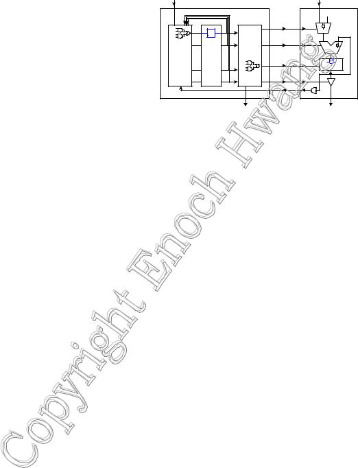
The car security system example from section 2.8 is an example of a combinational circuit. In the example, the siren is turned on when the master switch is on and someone opens the door. If you close the door then the siren will turn off immediately. For a more realistic car security system, we would like the
siren to remain on even after you close the door back after it is first triggered. In order for this modified
system to work correctly, the siren must be dependent not only on the master switch and the door switch, but also on whether the siren is currently on or off. In other words, this modified system is a sequential circuit that is dependent on both the current and past inputs.
The dependence of past input values implies the need for memory elements in order to remember this history of inputs. Sequential circuits, however, are just like combinational circuits in the sense that they are made up of the same basic logic gates. What makes them different is in the way these logic gates are connected. In order for the circuit to “remember” its current value, we have to connect the output of a logic gate directly or indirectly back to the input of that same gate. We call this a feedback loop circuit and it forms the basis for all memory elements. Combinational circuits do not have any feedback loops.
Latches and flip-flops are the basic elements for storing information. They are the fundamental building blocks for all sequential circuits. A latch or flip-flop can store one bit of information. The main difference between latches and flip-flops is that for latches, their outputs are constantly affected by their inputs as long as the enable signal is asserted. In other words, when they are enabled, their content changes immediately when their inputs change. Flipflops, on the other hand, have their content change only either at the rising or falling edge of the enable signal. After the rising or falling edge of the enable signal and during the time when the signal is at a constant 1 or 0, the flipflop’s content remains constant even if the input changes. This enable signal is usually the controlling clock signal. In this chapter, we will look at how latches and flip-flops are designed and how they work. There are also different variations of flip-flops that enhance their operations.
Historically, there are basically four main types of flip-flops: SR, D, JK, and T. The major differences between them are the number of inputs they have and how their contents change. Any given sequential circuit can be built using any of these types of flip-flops or combinations of them. However, selecting one type of flip-flop over another type to use in a particular circuit can affect the overall size of the circuit. Today, sequential circuits are designed with only D flip-flops because of their ease of use. We will thus focus only on the D flip-flop. Discussion on the other types of flip-flops can be found at the end of this chapter.
6.1 Bistable Element
Let us look at the inverter. If you provide the inverter input with a 1, the inverter will output a 0. If you remove the input, the inverter will not output a value. If you want to construct a memory circuit using the inverter, you would want the inverter to continue to output a 0 even after you remove the input. In order for the inverter to continue to output a 0, you need the inverter to self provide its own input. In other words, you want the output to feed back the 0 to the input. However, you cannot connect the output of the inverter directly to its input because you will have a 0 connected to a 1, and so creating a short circuit. The solution is to connect two inverters as shown in Figure 1 (a). This circuit is called a bistable element and is the simplest memory circuit.
Microprocessor Design – Principles and Practices with VHDL |
Last updated 7/21/2003 12:48 PM |
Chapter 6 – Latches and Flip-Flops |
Page 3 of 27 |
Q
|
|
|
|
Q' |
|
|
|
|
|
(a) |
|
Vout1 |
5 |
stable |
|
|
|
|
|
|
metastable |
||
= Vin2 |
|
metastable |
|
||
|
|
|
|
|
|
|
|
|
stable |
stable |
stable |
|
0 |
|
|
|
|
|
|
|
|
|
|
|
0 |
Vin1 |
5 |
|
|
|
|
= Vout2 |
|
(c) |
|
|
|
|
|
|
|
(b)
Figure 1. Bistable element: (a) circuit; (b) analog analysis; (c) ball and hill analogy for metastable behavior.
The bistable element has no primary inputs. It has two outputs labeled Q and Q’. Since the circuit has no inputs, we cannot change the values of Q and Q’. However, Q will take on whatever value it happens to be when the circuit is first powered up. Assume that Q = 0 when we switch on the power. Since Q is also the input to the bottom inverter, Q’, therefore, is a 1. A 1 going to the input of the top inverter will produce a 0 at the output Q, which is what we started off with. Similarly, if we start the circuit with Q = 1, we will get Q’ = 0, and again we get a stable situation.
A bistable element has memory in the sense that it can remember the content (or state) of the circuit indefinitely. Using the signal Q as the state variable, we say that the state of the circuit is the value that is stored in Q. Thus, the circuit has two stable states: Q = 0, and Q = 1; hence the name “bistable.”
An analog analysis of a bistable element, however, reveals that it has three equilibrium points and not just two stable states as found from the above digital analysis. Assuming again that Q = 1, and we plot the output voltage
(Vout1) versus the input voltage (Vin1) of the top inverter, we get the solid line in Figure 1 (b) The dotted line shows the operation of the bottom inverter where Vout2 and Vin2 are the output and input voltages respectively for that
inverter.
Figure 1 (b) shows that there are three intersection points, two of which correspond to the two stable states of the circuit where Q is either 0 or 1. The third intersection point labeled metastable, is at a voltage that is neither a logical 1 nor a logical 0 voltage. Nevertheless, if we can get the circuit to operate at this voltage, then it can stay at that point indefinitely. Practically, however, we can never operate a circuit precisely at a certain voltage. A slight deviation from the metastable point as cause by noise in the circuit or other stimulants will cause the circuit to go to one of the two stable points. Once at the stable point, a slight deviation, however, will not cause the circuit to go away from the stable point but rather back towards the stable point because of the feedback effect of the circuit.
An analogy of the metastable behavior is a ball on top of a symmetrical hill as depicted in Figure 1 (c). The ball can stay indefinitely in that precarious position as long as there is absolutely no movement whatsoever. With any slight force, the ball will roll down to either of the two sides. Once at the bottom of the hill, the ball will stay there until an external force is applied to it. The strength of this external force will cause the ball to do one of three things. If a small force is applied to the ball, it will go partly up the hill and then rolls back down to the same side. If a big enough force is applied to it, it will go over the top and down the other side of the hill. We can also apply a force that is just strong enough to push the ball to the top of the hill. Again at this precarious position, it can roll down either side.
We will find that all latches and flip-flops have this metastable behavior. In order for the element to change state, we need to apply a strong enough pulse satisfying a given minimum time requirement. Otherwise, the element will either remain at the current state or go into the metastable state in which case unpredictable results can occur. A
Microprocessor Design – Principles and Practices with VHDL |
Last updated 7/21/2003 12:48 PM |
Chapter 6 – Latches and Flip-Flops |
Page 4 of 27 |
study in the electrical characteristics of digital circuits is beyond the scope of this book. The interested reader is referred to the references.
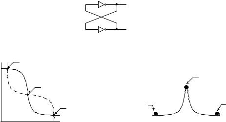
6.2 SR Latch
The bistable element is able to remember or store one bit of information. However, because it does not have any external inputs, we cannot change the bit that is stored in it. Whatever value Q contains when power is first applied to the circuit, the circuit will remain in that state indefinitely until power is removed. We cannot simply connect an external input to one of the inverter inputs because we can create a short circuit by connecting a 0 to a 1. For example, lets assume that the external input is connected to the input of the top inverter in Figure 1 (a) and that the current state of the circuit is 1, i.e. Q = 1. This implies that the input to the top inverter must be a 0. If we want to change the state to 0, then we must set the external input, which is connected to the input of the top inverter, to a 1. By doing this, the input to the top inverter will be momentarily shorted.
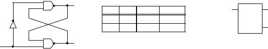
In order to change the information bit, we need to add external inputs to the circuit. The simplest way to add inputs is to replace the two inverters with two NAND gates as shown in Figure 2 (a). This circuit is called a SR latch. In addition to the two outputs Q and Q’, there are two inputs S' and R' for set and reset respectively. The SR latch can be in one of two states: a set state when Q = 1, or a reset state when Q = 0. Following the convention, the primes in S and R denote that these inputs are active low, i.e. a 0 asserts them and a 1 de-asserts them.
To make the SR latch go to the set state, we simply assert the S' input by setting it to 0. It doesn’t matter what the other NAND gate input is because 0 NAND anything gives a 1, hence Q = 1 and the latch is set. If S' remains at a 0 so that Q (which is connected to one input of the bottom NAND gate) remains at a 1, if we now de-assert R', i.e. R' = 1, then the output of the bottom NAND gate will be a 0, and so Q' = 0. This situation is shown in Figure 2 (d) at time t0. From this current situation, if we now de-assert S' so that S' = R' = 1, the latch will remain in the set state because Q', the second input to the top NAND gate, is 0 which will keep Q = 1 as shown at time t1. At time t2 we reset the latch by making R' = 0. With R' being a 0, Q' will go to a 1. At the top NAND gate, 1 NAND 1 is 0, thus forcing Q to go to a 0. If we de-assert R' so that again we have S' = R' = 1, this time the latch will remain in the reset state as shown at time t3.
Notice the two times (at t1 and t3) when both S' and R' are de-asserted (S' = R' = 1). At t1, Q is at a 1, whereas, at t3, Q is at a 0. Why is this so? What is different between these two times? The difference is in the value of Q immediately before those times. The value of Q right before t1 is a 1, whereas the value of Q right before t3 is a 0. When both inputs are de-asserted, the SR latch remembers its previous state. Previous to t1, Q has the value 1, so at t1, Q remains at a 1. Similarly, previous to t3, Q has the value 0, so at t3, Q remains at a 0.
S'
R'
Figure 2. SR latch:
|
|
|
|
|
|
|
|
Q |
|
S' |
R' |
|
Q |
|
Qnext |
Qnext' |
|
||||
|
|
|
|
|
|
|
|
||||||||||||||
|
|
|
|
|
|
|
|
|
0 |
|
0 |
× |
|
1 |
1 |
|
|||||
|
|
|
|
|
|
|
|
|
|
|
|
|
|||||||||
|
|
|
|
|
|
|
|
|
|
0 |
|
1 |
× |
|
1 |
0 |
|
||||
|
|
|
|
|
|
|
|
|
|
1 |
|
0 |
× |
|
0 |
1 |
|
||||
|
|
|
|
|
|
|
|
Q' |
|
1 |
|
1 |
0 |
|
0 |
1 |
|
||||
|
|
|
|
|
|
|
|
||||||||||||||
|
|
|
|
|
|
|
|
|
1 |
|
1 |
1 |
|
1 |
0 |
|
|||||
|
|
|
(a) |
|
|
|
|
|
|
|
|
||||||||||
|
|
|
|
|
|
|
|
|
|
|
|
|
|
(b) |
|
|
|
||||
|
|
|
|
|
|
|
|
|
S' |
|
|
|
|
|
|
|
|
|
|
|
|
|
|
|
|
|
|
|
|
|
|
|
|
|
|
|
|
|
|
|
|
||
|
|
S' |
Q |
|
|
|
|
|
|
|
|
|
|
|
|
|
|
|
|||
|
|
|
|
|
|
|
|
|
|
|
|
|
|
|
|
||||||
|
|
|
|
R' |
|
|
|
|
|
|
|
|
|
|
|||||||
|
|
|
|
|
|
|
|
|
|
|
|
|
|
|
|
|
|
|
|||
|
|
|
|
|
|
|
|
|
|
|
|
|
|
|
|
|
|
|
|
|
|
|
|
R' |
Q' |
|
|
Q |
|
|
|
|
|
|
|
|
Undefined |
||||||
|
|
|
|
|
|
|
|
|
|
||||||||||||
|
|
|
|
Q' |
|
|
|
|
|
|
|
|
|
|
|||||||
|
|
|
|
|
|
|
|
|
|
|
|
|
|
|
|
|
|
||||
|
|
|
|
|
|
|
|
|
|
|
|
|
|
|
|
|
|
||||
|
|
|
|
|
|
|
|
|
|
|
|
|
|
|
|
|
Undefined |
||||
|
|
|
(c) |
|
|
|
|
t0 t1 |
t2 |
t3 |
t4 t5 |
t6 |
|||||||||
(d)
(a) circuit using NAND gates; (b) truth table; (c) logic symbol; (d) timing diagram.
Microprocessor Design – Principles and Practices with VHDL |
Last updated 7/21/2003 12:48 PM |
Chapter 6 – Latches and Flip-Flops |
Page 5 of 27 |
If both S' and R' are asserted (set to a 0), then both Q and Q' are equal to a 1 as shown at time t4, since 0 NAND anything gives a 1. Note that there is nothing wrong with having Q equals to Q'. It is just because we named these two points Q and Q' that we don’t like them to be equal. But we could have used the name P instead of Q'.
If one of the input signals is de-asserted earlier than the other, the latch will end up in the state forced by the signal that is de-asserted later as shown at time t5. At t5, R' is de-asserted first, so the latch goes into the set state with Q = 1 and Q' = 0.
A problem exists if both S' and R' are de-asserted at exactly the same time as shown at time t6. Let us assume for a moment that both gates have exactly the same delay and that the two wire connections between the output of one gate to the input of the other gate also have exactly the same delay. Currently, both Q and Q' are at a 1. If we set S' and R' to a 1 at exactly the same time, then both NAND gates will perform a 1 NAND 1, and will both output a 0 at exactly the same time. The two zeros will be fed back to the two gate inputs at exactly the same time because the two wire connections have the same delay. This time round, the two NAND gates will perform a 1 NAND 0, and will both produce a 1, again at exactly the same time. This time, two ones will be fed back to the inputs, which again will produce a 0 at the outputs, and so on and on. This oscillating behavior, called the critical race, will continue forever until one out paces the other. If the two gates do not have exactly the same delay then the situation is similar to de-asserting one input before the other, and so the latch will go into one state or the other. However, since we do not know which is the faster gate, therefore, we do not know which state the latch will end up in. Thus, the latch’s next state is undefined.
Of course, in practice, it is next to impossible to manufacture two gates and make the two connections with precisely the same delay. In addition, both S' and R' need to be de-asserted at exactly the same time. Nevertheless, if this circuit is used in controlling the space shuttle, we don’t want even this slim chance to happen.
In order to avoid this non-deterministic behavior, we must make sure that the two inputs are never de-asserted at the same time. Note that we do want the situation when both of them are de-asserted as in times t1 and t3 so that the circuit can remember its current content. We want to de-assert one input after de-asserting the other, but just not deasserting both of them at exactly the same time. In practice, it is very difficult to guarantee that these two signals are never de-asserted at the same time, so we relax the condition slightly by not having both of them asserted together. In other words, if one is asserted, then the other one cannot be asserted. So if both of them are never asserted, then they can’t be de-asserted at the same time. A minor side benefit for not having both of them asserted together is that Q and Q' are never equal to each other. Recall that from the names that we have given these two nodes, we do want them to be inverses of each other.
From the above analysis, we obtain the truth table in Figure 2 (b) for the NAND implementation of the SR latch.
In the truth table, Q and Qnext actually represent the same point in the circuit. The difference is that Q is the current state or the current content of the latch and Qnext is the value to be updated in the next state or next time period. Q is the input to a gate and is the output from a gate. So the value of Q goes into a gate, and after this signal
propergates through the two gates and arrives back at Q then this new signal is referred to as Qnext. Figure 2 (c) shows the logic symbol for the SR latch.
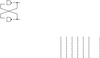
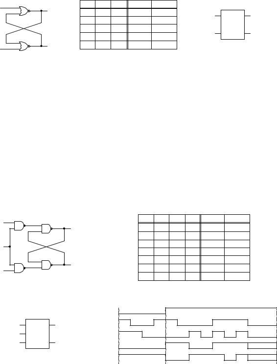
The SR latch can also be implemented using NOR gates as shown in Figure 3 (a). The truth table for this implementation is shown in Figure 3 (b). From the truth table, we see that the main difference between this implementation and the NAND implementation is that for the NOR implementation, the S and R inputs are active high, so that setting S to 1 will set the latch and setting R to 1 will reset the latch. However, just like the NAND implementation, the latch is set when Q = 1 and reset when Q = 0. The latch remembers its previous state when S = R = 0. When S = R = 1, both Q and Q' are 0. The logic symbol for the SR latch using NOR implementation is shown in Figure 3 (c).
Microprocessor Design – Principles and Practices with VHDL |
Last updated 7/21/2003 12:48 PM |
Chapter 6 – Latches and Flip-Flops
R |
Q |
S |
R |
Q |
Qnext |
Qnext' |
|
0 |
0 |
0 |
0 |
1 |
|||
|
|||||||
|
|
0 |
0 |
1 |
1 |
0 |
|
|
|
0 |
1 |
× |
0 |
1 |
|
|
|
1 |
0 |
× |
1 |
0 |
|
S |
Q' |
1 |
1 |
× |
0 |
0 |
|
|
|
|
|
|
|
||
|
(a) |
|
|
|
(b) |
|
|
|
|
|
|
|
|
Figure 3. SR latch: (a) circuit using NOR gates; (b) truth table; (c) logic symbol.
Page 6 of 27
S Q
R Q'
(c)
6.3 SR Latch with Enable
The SR latch is sensitive to its inputs all the time. In other words, Q will always change when either S or R is asserted. It is sometimes useful to be able to disable the inputs so that asserting them will not cause the latch to change state, but to keep its current state. Of course, this is achieved by de-asserting both S and R. So what we want is just one enable signal that will de-assert both S and R. The SR latch with enable (also known as a gated SR latch) shown in Figure 4 (a) accomplishes this by adding two extra NAND gates to the original NAND gate implementation of the latch. These two new NAND gates are controlled by the enable input, E, which determines whether the latch is enabled or disabled. When E = 1, the circuit behaves like the normal NAND implementation of the SR latch except that the new S and R inputs are active high rather than active low. When E = 0, then S' = R' = 1, and the latch will remain in its previous state regardless of the S and R inputs. The truth table for the SR latch with enable is shown in Figure 4 (b), and its logic symbol in Figure 4 (c).
A typical operation of the latch is shown in the timing diagram in Figure 4 (d). Between t0 and t1, E = 0 so changing the S and R inputs do not affect the output. Between t1 and t2, E = 1 and the trace is similar to the trace of Figure 2 (d) except that the input signals are inverted.
S |
S' |
|
E |
S |
R |
Q |
Qnext |
Qnext' |
|
Q |
0 |
× |
× |
0 |
0 |
1 |
|||
|
|
||||||||
|
|
|
0 |
× |
× |
1 |
1 |
0 |
|
E |
|
|
1 |
0 |
0 |
0 |
0 |
1 |
|
|
|
1 |
0 |
0 |
1 |
1 |
0 |
||
|
|
|
|||||||
|
|
Q' |
1 |
0 |
1 |
× |
0 |
1 |
|
R |
|
1 |
1 |
0 |
× |
1 |
0 |
||
R' |
|
||||||||
|
1 |
1 |
1 |
× |
1 |
1 |
|||
|
|
|
|||||||
|
|
(a) |
|
|
|
(b) |
|
|
|
|
|
|
|
|
|
|
|
||
|
|
|
E |
|
|
|
|
|
|
|
S |
Q |
S |
|
|
|
|
|
|
|
E |
|
R |
|
|
|
|
|
|
|
R |
Q' |
Q |
|
|
|
|
Undefined |
|
|
|
|
|
|
|
|
|||
|
|
(c) |
Q' |
|
|
|
|
Undefined |
|
|
|
t0 |
|
t1 |
|
|
t2 |
||
|
|
|
|
|
|
(d)
Figure 4. SR latch with enable: (a) circuit using NAND gates; (b) truth table; (c) logic symbol; (d) sample timing diagram.
Microprocessor Design – Principles and Practices with VHDL |
Last updated 7/21/2003 12:48 PM |
Chapter 6 – Latches and Flip-Flops |
Page 7 of 27 |
6.4 D Latch
Recall from section 6.2 that the disadvantage with the SR latch is that we need to ensure that the two inputs, S and R, are never de-asserted at exactly the same time and we said that we can guarantee this by not having both of them asserted. This situation is prevented in the D latch by adding an inverter between the original S' and R' inputs. This way, S' and R' will always be inverses of each other, and so they will never be both asserted. The circuit using NAND gates and the inverter is shown in Figure 5 (a). There is now only one input D (for data). When D = 0, then S' = 1 and R' = 0, so this is like resetting the SR latch by making Q = 0. Similarly, when D = 1, then S' = 0 and R' = 1,
and Q will be set to a 1. From this observation, we see that Qnext always gets the same value as the input D, and is independent of the current value of Q. Hence, we obtain the truth table for the D latch as shown in Figure 5 (b).
Comparing the truth table for the D latch shown in Figure 5 (b) with the truth table for the SR latch shown in Figure 2 (b), it is obvious that we have eliminated not just one, but three rows where S' = R'. The reason for adding the inverter to the SR latch circuit was to eliminate the row where S' = R' = 0. However, we still need to have the other two rows where S' = R' = 1 in order for the circuit to remember its current value. By not being able to set both
S' and R' to 1, this D latch circuit has now lost its ability to remember. Qnext cannot remember the current value of Q but will always follow D.
S'
|
|
Q |
D |
Q |
Qnext |
Qnext' |
D Q |
|
|
|
|||||
|
|
|
0 |
× |
0 |
1 |
|
|
|
|
1 |
× |
1 |
0 |
Q' |
D |
R' |
Q' |
|
|
(b) |
|
(c) |
|
|
|
|
|
|
(a)
Figure 5. D latch: (a) circuit using NAND gates; (b) truth table; (c) logic symbol.
6.5 D Latch with Enable
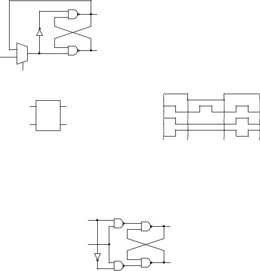
In order to make the D latch remember the current value, we need to loop back the current value of Q to the D input. Another way of looking at it is like adding the enable input to the SR latch so that when the latch is disabled, the inputs will not affect the current value in Q, but rather the latch will maintain its current value. To achieve this, we can use a 2-input multiplexer to select whether to pass the external D input or loop back the current value of Q to the circuit at the point of the original D. The output of the multiplexer is connected to the original D input, and the select line of the multiplexer is connected to the enable input E. The D latch with enable circuit is shown in Figure 6 (a).
When the enable input E is asserted (E = 1), the D input passes through the multiplexer and so the Q output follows the D input. On the other hand, when E is de-asserted (E = 0), the current value of Q loops back as the input to the circuit and so Qnext (i.e., the output Q) retains its last value independent of the D input.
When the latch is enabled, the latch is said to be open and the path from the input D to the output Q is transparent. In other words, Q follows D. Because of this characteristic, the D latch with enable circuit is often referred to as a transparent latch. When the latch is disabled, it is closed, and the latch remembers its current state. The truth table and the logic symbol for the D latch with enable are shown in Figure 6 (b) and (c). A sample timing diagram for the operation of the D latch with enable is shown in Figure 6 (d). Between t0 and t1, the latch is enabled with E = 1 so the output Q follows the input D. Between t1 and t2, the latch is disabled, so Q remains stable even when D changes.
Microprocessor Design – Principles and Practices with VHDL |
Last updated 7/21/2003 12:48 PM |
Chapter 6 – Latches and Flip-Flops |
Page 8 of 27 |
|
|
S' |
|
Q |
|
|
|
|
|
|
0 |
R' |
|
Q' |
D |
1 sy |
|
|
|
|
E |
(a) |
|
|
|
|
|
|
|
|
|
|
|
E |
|
|
D |
Q |
D |
|
|
E |
Q' |
Q |
|
|
|
||
|
|
|
|
Q' |
E |
D |
Q |
Qnext |
Qnext' |
0 |
× |
0 |
0 |
1 |
0 |
× |
1 |
1 |
0 |
1 |
0 |
× |
0 |
1 |
1 |
1 |
× |
1 |
0 |
(b)
(c) |
t0 |
t1 |
t2 |
t3 |
(d)
Figure 6. D latch with enable: (a) circuit; (b) truth table; (c) logic symbol; (d) sample timing diagram.
An alternative way for constructing the D latch with enable circuit is shown in Figure 7. Instead of using the 2- input multiplexer as in Figure 6 (a), we start with the SR latch with enable circuit of Figure 4 (a) and connect the S and R inputs together with an inverter. The functional operations of these two circuits are identical.
D |
S |
S' |
|
||
|
|
Q |
E |
|
|
Q'
R R'
Figure 7. D latch with enable circuit using four NAND gates.
6.6 Clock
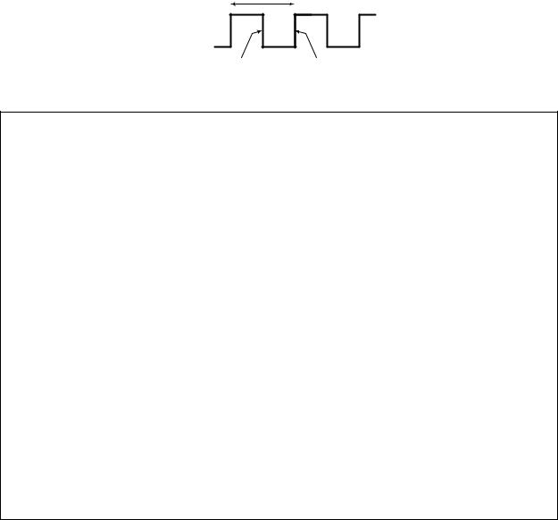
Latch circuits are known as level-sensitive because their outputs are affected by their inputs as long as they are enabled. Their memory state can change during this entire time when the enable signal is asserted. In a computer circuit, however, we do not want the memory state to change at various times when the enable signal is asserted. Instead we like to synchronize all the state changes to happen at precisely the same moment and at regular intervals. In order to achieve this, two things are needed: 1) a synchronizing signal, and 2) a memory circuit that is not levelsensitive. The synchronizing signal, of course, is the clock, and the non-level-sensitive memory circuit is the flipflop.
The clock is simply a very regular square wave signal as shown in Figure 8. We call the portion of the clock signal when it changes from a 0 to a 1 the rising edge. Conversely, the falling edge of the clock is the portion when the signal changes from a 1 to a 0. We will use the symbol to denote the rising edge and for the falling edge. In a computer circuit, either the rising edge or the falling edge of the clock is used as the synchronizing signal for writing data into a memory element. This edge signal is referred to as the active edge of the clock. In all our examples where needed, we will use the rising edge of the clock as the active edge. So at every rising edge, data will
Microprocessor Design – Principles and Practices with VHDL |
Last updated 7/21/2003 12:48 PM |
Chapter 6 – Latches and Flip-Flops |
Page 9 of 27 |
be clocked or stored into the memory element.
A clock cycle is the time from one rising edge to the next rising edge or from one falling edge to the next falling edge. The speed of the clock, measured in hertz (Hz), is the number of cycles per second. Typically, the clock speed for a microprocessor in an embedded system runs between 4MHz to 20MHz, while the microprocessor in a personal computer runs upwards of 2GHz. A clock period is the time for one clock cycle (seconds per cycle) so it is just the inverse of the clock speed.
The speed of the clock is determined by how fast a circuit can produce valid results. For example, a two-level combinational circuit will have valid result at its output much sooner than say an ALU can. Of course, we want the clock speed to be as fast as possible, but it can only be as fast as the slowest circuit in the entire system. We want the clock period to be the time it takes for the slowest circuit to get its input from a memory element, operate on the data, and then writes the data back into a memory element. More will be said on this in section 8.3.
Figure 9 shows a VHDL description of a clock divider circuit that roughly cuts a 25MHz clock down to 1Hz.
one clock cycle
Falling edge |
Rising edge |
Figure 8. Clock signal.
LIBRARY IEEE;
USE IEEE.STD_LOGIC_1164.all;
ENTITY clockdiv IS PORT ( clock_25Mhz: IN STD_LOGIC; clk: OUT STD_LOGIC);
END clockdiv;
ARCHITECTURE Behavior OF clockdiv IS CONSTANT max: INTEGER := 25000000; CONSTANT half: INTEGER := max/2; SIGNAL count: INTEGER RANGE 0 TO max; SIGNAL toggle: STD_LOGIC;
BEGIN PROCESS BEGIN
WAIT UNTIL clock_25Mhz'EVENT and clock_25Mhz = '1'; IF count < max THEN
count <= count + 1; ELSE
count <= 0; END IF;
IF count < half THEN toggle <= '0';
ELSE
toggle <= '1'; END IF;
clk <= toggle; END PROCESS;
END Behavior;
Figure 9. VHDL behavioral description of a clock divider circuit.
Microprocessor Design – Principles and Practices with VHDL |
Last updated 7/21/2003 12:48 PM |
Chapter 6 – Latches and Flip-Flops |
Page 10 of 27 |
6.7 D Flip-Flop
Unlike the latch, a flip-flop is not level-sensitive, but rather edge-triggered. In other words, data gets stored into a flip-flop only at the active edge of the clock. An edge-triggered flip-flop achieves this by combining in series a pair of latches. Figure 10 (a) shows a positive-edge-triggered D flip-flop where two D latches are connected in series. A clock signal Clk is connected to the E input of the two latches, one directly, and one through an inverter.
The first latch is called the master latch. The master latch is enabled when Clk = 0 because of the inverter, and so QM follows the primary input D. However, the value of QM cannot pass over to the primary output Q because the second latch is disabled when Clk = 0. When Clk = 1, the master latch is disabled but the second latch, called the slave latch, is enabled so that the output from the master latch QM is transferred to the slave latch at Q. The slave latch is enabled all the while that Clk = 1, but its content changes only at the rising edge of the clock because once Clk is 1, the master latch is disabled and so the input to the slave latch QM will be stable. So when Clk = 1 and the slave latch is enabled, the output Q will not change because the input QM is not changing.
The circuit of (a) is called a positive edge-triggered D flip-flop because the primary output Q on the slave latch changes only at the rising edge of the clock. If the slave latch is enabled when the clock is low (i.e., with the inverter output connected to the E of the slave latch), then it is referred to as a negative edge-triggered flip-flop. The circuit is also referred to as a master-slave D flip-flop because of the two latches used in the circuit.
Figure 10 (b) shows the truth table for the D flip-flop. The symbol signifies the rising edge of the clock.
When Clk is either at a 0 or a 1, the flip-flop retains its current value, i.e., Qnext = Q. Qnext changes and follows the primary input D only at the rising edge of the clock. The logic symbol for the positive-edge-triggered D flip-flop is
shown in (c). The small triangle at the clock input indicates that the circuit is triggered by the edge of the signal and so it is a flip-flop. Without the small triangle, the symbol would be for a latch. If there is a circle in front of the clock line, then the flip-flop is triggered by the falling edge of the clock making it a negative-edge-triggered flip-flop. Figure 10 (d) shows a sample trace diagram for the D flip-flop. Notice that when Clk = 0, QM follows D and the output of the slave latch Q remains constant. On that other hand, when Clk = 1, Q follows QM and the output of the master latch QM remains constant.
|
|
|
|
|
|
|
|
|
|
|
|
|
|
|
|
|
Clk |
|
D |
|
|
Q |
|
|
Qnext |
|
|
Qnext' |
||||||||||||||
|
|
|
|
|
|
|
QM |
|
|
|
|
|
|
0 |
|
|
× |
|
|
0 |
|
|
0 |
|
|
1 |
|
|||||||||||||||
D |
|
|
D |
Q |
|
D |
Q |
|
Q |
|
0 |
|
|
× |
|
|
1 |
|
|
1 |
|
|
0 |
|
||||||||||||||||||
|
|
|
|
|
|
|
|
|
|
|
|
|
|
|
|
|
|
|||||||||||||||||||||||||
|
|
|
E |
Q' |
|
|
|
|
E |
Q' |
|
Q' |
|
1 |
|
|
× |
|
|
0 |
|
|
0 |
|
|
1 |
|
|||||||||||||||
|
|
|
|
|
|
|
|
|
1 |
|
|
× |
|
|
1 |
|
|
1 |
|
|
0 |
|
||||||||||||||||||||
|
|
|
|
|
|
|
||||||||||||||||||||||||||||||||||||
|
|
|
|
|
|
|
||||||||||||||||||||||||||||||||||||
Clk |
|
|
Master |
|
|
|
|
|
|
|
Slave |
|
|
|
|
0 |
|
|
× |
|
|
|
0 |
|
|
1 |
|
|||||||||||||||
|
|
|
|
|
|
|
|
|
|
|
||||||||||||||||||||||||||||||||
|
|
|
|
|
|
|
|
|
|
|
|
|
|
|
|
|
1 |
|
|
× |
|
|
|
1 |
|
|
0 |
|
||||||||||||||
|
|
|
|
|
|
|
|
|
|
|
|
|
|
|
|
|
|
|
|
|
|
|
|
|
||||||||||||||||||
|
|
|
|
|
|
(a) |
|
|
|
|
|
|
|
|
|
|
|
|
|
|
|
|
|
|
|
|
|
(b) |
|
|
|
|
|
|
|
|
|
|
|
|||
|
|
|
|
|
|
|
|
|
|
|
|
|
|
|
|
|
|
|
|
|
|
|
|
|
|
|
|
|
|
|
|
|
|
|
|
|
|
|
|
|||
|
|
|
|
|
|
|
|
|
|
|
|
|
|
|
|
Clk |
|
|
|
|
|
|
|
|
|
|
|
|
|
|
|
|
|
|
|
|
|
|
|
|
||
|
|
|
|
|
|
|
|
|
|
|
|
|
|
|
|
|
|
|
|
|
|
|
|
|
|
|
|
|
|
|
|
|
|
|
|
|
|
|
||||
|
|
|
|
|
|
|
|
|
|
|
|
|
|
|
|
|
|
|
|
|
|
|
|
|
|
|
|
|
|
|
|
|
|
|
|
|
|
|
|
|
|
|
|
|
|
|
|
D |
|
|
Q |
|
|
|
|
|
|
|
D |
|
|
|
|
|
|
|
|
|
|
|
|
|
|
|
|
|
|
|
|
|
|
|
|
||
|
|
|
|
|
|
|
|
|
|
|
|
|
|
|
|
|
|
|
|
|
|
|
|
|
|
|
|
|
|
|
|
|
|
|
|
|
|
|||||
|
|
|
|
|
Clk Q' |
|
|
|
|
|
|
QM |
|
|
|
|
|
|
|
|
|
|
|
|
|
|
|
|
|
|
|
|
|
|
|
|
||||||
|
|
|
|
|
|
|
|
|
|
|
|
|
|
|
|
|
|
|
|
|
|
|
|
|
|
|
|
|
|
|
|
|
|
|||||||||
|
|
|
|
|
|
|
|
|
|
|
|
Q |
|
|
|
|
|
|
|
|
|
|
|
|
|
|
|
|
|
|
|
|
|
|
|
|
||||||
|
|
|
|
|
|
|
|
|
|
|
|
|
|
|
|
|
|
|
|
|
|
|
|
|
|
|
|
|
|
|
|
|
|
|
|
|||||||
|
|
|
|
|
|
|
|
|
|
|
|
|
|
|
|
|
|
|
|
|
|
|
|
|
|
|
|
|
|
|
|
|
|
|
|
|
|
|
|
|
||
|
|
|
|
|
|
|
|
|
|
|
|
|
|
|
|
|
|
|
|
|
|
|
|
|
|
|
|
|
|
|
|
|
|
|
|
|
|
|
|
|
||
|
|
|
|
|
|
(c) |
|
|
|
|
|
|
|
|
|
t0 |
|
t1 |
|
|
|
|
|
|
|
t2 |
|
|
|
|
t3 |
|||||||||||
|
|
|
|
|
|
|
|
|
|
|
|
|
|
|
|
|
|
|
|
|
|
|
|
|
|
|
|
|
(d) |
|
|
|
|
|
|
|
|
|
|
|
||
Figure 10. Master-slave positive-edge triggered D flip-flop: (a) circuit using D latches; (b) truth table; (c) logic symbol; (d) trace diagram.
Another way of constructing a positive-edge-triggered flip-flop is to use three interconnected SR latches rather than a master and a slave D latch. The circuit is shown in Figure 11. The advantage of this circuit is that it uses only 6 NAND gates (26 transistors) as opposed to 10 gates (46 transistors) for the master-slave D flip-flop of Figure 10
(a). The operation of the circuit is as follows. When Clk = 0, the outputs of gates 2 and 3 are high (0 NAND x = 1).
Microprocessor Design – Principles and Practices with VHDL |
Last updated 7/21/2003 12:48 PM |