

06.Transmission line transformers
.pdfBALUNS 115
The SPICE net list used to analyze this circuit makes use of the conversion of voltages to S parameters:
Analysis of a circuit for S11 and S21
*
*R01 and R02 are input and output resistance levels.
*RL is the load resistance. The load may be supplemented
*with additional elements.
*.PARAM R01=50, R02=50. RLOAD=50. IN1=-1/R01
.PARAM R01=50, |
R02=200. RLOAD=200. IIN=-1/R01 |
||||
.FUNC |
N(R01,R02) SQRT(R02/R01) |
||||
R01 |
1 |
0 |
R01 |
|
|
VIN |
10 |
11 |
AC |
1 |
|
GI1 |
1 |
0 |
VALUE=-V(10,11)/R01 |
||
*GI1 |
1 |
0 |
10 |
11 |
”-1/R01” |
E11 |
10 |
0 |
1 |
0 |
2 |
R11 |
11 |
0 |
1 |
|
|
Xcircuit |
1 |
2 |
TLTCKT |
||
RL |
2 |
0 |
RLOAD |
|
|
E21 |
21 |
0 |
VALUE=V(2)*2/N(R01,R02) |
||
*n = SQRT(R02/R01)
*E21 |
21 |
0 |
2 |
0 |
”2/n” |
R21 |
21 |
0 |
1 |
|
|
* |
|
|
|
|
|
.SUBCKT TLTCKT |
1 |
4 |
|
||
*Input side
*4 cm = .1333 wavelength at 1 GHz
TLT4 |
1 |
0 |
4 |
1 |
Z0=200 F=1GHz NL=.1333 |
* Output |
side |
|
|
|
|
.ENDS |
|
TLTCKT |
|
|
|
* Code for S11 |
and |
S21 |
|
||
*.AC DEC |
”num” |
”f1” |
”f2” |
||
.AC |
LIN |
301 |
.1MEG |
2GHZ |
|
.PROBE V(11) |
V(21) |
|
|
||
.END |
|
|
|
|
|
6.5BALUNS
A balun (balanced–unbalanced) is a circuit that transforms a balanced transmission line to an unbalanced transmission. An example of a balanced line is the two-wire transmission line. An unbalanced line is one where one of the lines is grounded, such as in coaxial line or microstrip. One situation where this is important is in feeding a dipole antenna with a coaxial line where the antenna

116 TRANSMISSION LINE TRANSFORMERS
is balanced and the coaxial line is unbalanced. One simple structure is shown in Fig. 6.11 where the difference between the inputs of the antenna is forced to be 180° by addition of a half wavelength line between them. At RF frequencies, a more practical way to perform this same function is to use a transmission line transformer as shown in the example of the 1 : 1 balun in Fig. 6.12a. There is no specified ground on the right-hand side of this circuit, but since the voltage difference on the input side is V, the voltage across the load must also be V.
Dipole Antenna |
+V |
–V |
|
Balun
Coax
Feed
Coax
λ /2 Line
FIGURE 6.11 Balun example used for dipole antenna.
|
|
+ |
V |
+ |
V |
|
||
– |
|
|
|
– |
|
|
|
(a )
+V |
Dipole Antenna |
–V |
Feed Line
(b )
FIGURE 6.12 (a) Transmission line transformer implementation of a 1 : 1 balun, and (b) grounding one side gives a CV and V to the two sides of the dipole antenna.

DIVIDERS AND COMBINERS |
117 |
|
|
|
|
|
|
|
|
|
|
|
|
|
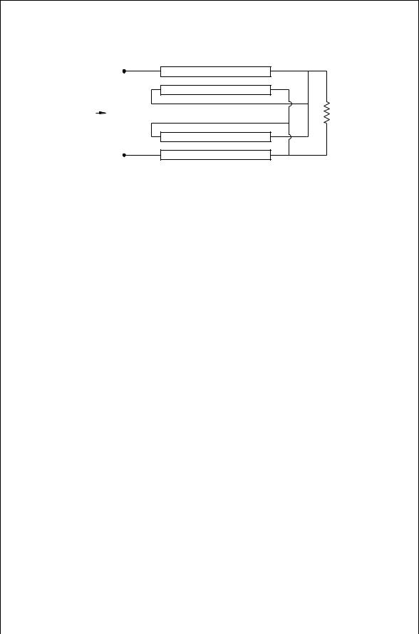
R G R L
FIGURE 6.13 A balun with a RG : RL D 1 : 4 impedance ratio.
For the dipole application, where a CV is needed on one side and V on the other side, one of the output sides can be grounded as indicated in Fig. 6.12b. The (RG : RL D 1 : 4) balun in Fig. 6.13 shows that impedance matching and changing to a balanced line can be accomplished with a balun. Analysis of this circuit may be aided by assuming some voltage, Vx, at the low side of RL. When the voltage at the upper side of RL is found, it also contains Vx. The difference between the lower and upper sides of RL removes the Vx.
6.6DIVIDERS AND COMBINERS
Transmission lines can be used to design power dividers and power combiners. These are particularly important in design of high-power solid state RF amplifiers where the input can be split between several amplifiers or where the outputs of several amplifiers may be effectively combined into one load. A very simple two-way power divider is shown in Fig. 6.14. In this circuit RL D 2RG, and the
V 1 |
2V 1 – V x |
I 1 / 2 |
I 1 |
|
|
|
|
|
R G |
|
R L |
V x |
V 1 |
R n |
|
|
|
|
|
R L |
|
|
I 1 / 2 |
FIGURE 6.14 A two-way power divider.

118 TRANSMISSION LINE TRANSFORMERS
p transmission line characteristic impedance is designed to be Z0 D 2RG. The
current in Rn ordinarily would be 0 because of equal voltages on either side of that resistance. Under unbalanced load conditions, Rn can absorb some of the unbalanced power and thus protect whatever the load is. When the two loads are both 2RG. The input voltage is V1 on the top conductor, and the voltage on the lower conductor is Vx on the left side. On the right-hand side the lower conductor is V1, and so the top conductor must be 2V1 Vx to ensure that both sides of the transmission line have the same voltage across the terminals, that is, V1 Vx. Since the current flowing through the upper load resistor and the lower load resistor must be the same, the voltage on either side of Rn is the same. Consequently 2V1 Vx D Vx or Vx D V1, so the voltage to current ratio at the
load is |
|
|
V1 |
D 2RG |
6.19 |
RL D I1/2 |
A two-way 180° power combiner shown in Fig. 6.15 makes use of a hybrid coupler and a balun. The resistor Rn is used to dissipate power when the two inputs are not exactly equal amplitude or exactly 180° out of phase so that matched loading for the two sources is maintained. For example, consider when I1 D I2, as shown in Fig. 6.15, so that I1 is entering the hybrid and I2 is leaving the hybrid. The current flowing through the load, RL, is I0. The current flowing into the hybrid transmission line from the top is I1 I0, while the current
V1 |
I o |
I 1 |
I 1 – I o |
I o
R L
R n
V 2  I o – I 2
Io
I 2
FIGURE 6.15 A two-way 180° power combiner.

DIVIDERS AND COMBINERS |
119 |
flowing from the bottom is I0 I2. The odd-mode current in the transmission line forces is
I1 I0 D I0 I2
or
I0 D I1 |
6.20 |
All the current goes through the balun, and no current flows through the hybrid. The current through Rn is therefore 0 leading to Vx D 0. The voltage difference between the two ends of the transmission lines of the hybrid is the same, which implies that
V1 Vx D Vx V2 |
|
||
or |
|
||
|
V1 D V2 |
6.21 |
|
and |
|
||
V0 D V1 V2 D 2V1 |
6.22 |
||
The matching load resistance is then |
|
||
|
V0 |
|
|
|
|
D RL D 2RG |
6.23 |
|
I0 |
||
When I1 and I2 are both entering the circuit so that I1 D I2, and V1 D V2, then voltages across the top and bottom of the transmission line in the hybrid circuit of Fig. 6.15 are
V1 Vx D Vx V2
or
Vx D V1 |
6.24 |
The voltage across the load is V0 D 0 and I0 D 0. The current in the hybrid transmission line is I1, so the current flowing through Rn is 2I1:
Rn D |
Vx |
|
V1 |
1 |
RG |
6.25 |
|
|
D |
|
D |
|
|||
2I1 |
2I1 |
2 |
|||||
The choices for RL and Rn ensure impedance matching for an arbitrary phase relationship between I1 and I2. Optimum performance would be expected if the characteristic impedances of the transmission lines were
p
Z0-balun D 2RG |
6.26 |
||
RG |
6.27 |
||
Z0-hybrid D p |
|
|
|
2 |
|||

120 TRANSMISSION LINE TRANSFORMERS
Rn |
Va |
|
Vd |
Rn |
Vb |
|
Va |
|
Vc |
Rn |
|
|
Vb |
|
Vd |
Rn |
|
|
Vc |
– |
+ |
+
R L V o
–
+
R L V o
–
+
R L V o
–
+
R L V o
–

 V 1 R G I 1
FIGURE 6.16 A four-way power divider.
The four-way power divider illustrated in Fig. 6.16 has some similarities with the Wilkinson power divider used at microwave frequencies. In the Wilkinson divider, matching impedances between the input and output is done by choosing
the quarter wavelength transmission lines to have a characteristic impedance p
Z0 D NRG, where N is the power division ratio, and Rn D RG. In the present circuit, impedance matching is done using an impedance transformer at the voltage source (not shown in Fig. 6.16). If it is desired that all the output loads and voltages be equal to one another, then it follows that the current in the Rn resistors is 0. This can be shown easily as follows: The voltage difference between the conductors on the right-hand side in each of the transmission lines is Vo V1. Then, for the left-hand side,
Vo V1 D Va Vd D Vb Va D Vc Vb D Vd Vc |
6.28 |
Combining the second and third expressions, then the third and fourth expressions, and so on, leads to the following:
2Va D Vb C Vd |
6.29 |
2Vb D Vc C Va |
6.30 |
2Vc D Vb C Vd |
6.31 |
REFERENCES 121
R in |
R L |
FIGURE 6.17 Transmission line transformer for Problem 6.1.
Equations (6.29) and (6.31) clearly show that Va D Vc, and Eq. (6.30) shows that Vb D Va and finally that Vd D Va. This means that there is no current flowing in the Rn resistors and that on the right-hand side, Vo D V1. The current entering each transmission line must then be I1/4, where I1 is the input current from the source. The load currents are also I1/4, so the impedance transformation at the input requires that RG D RL/4.
PROBLEMS
6.1Indicate the direction of the currents in the transmission line transformer shown in Fig. 6.17. Determine the value of Rin in terms of Rout.
6.2For the 4 : 1 transformer shown in Fig. 6.2, calculate the output power, Po D 1/2jI2j2RL, where the frequency dependence of the transmission lines is used. You will have three equations in the three unknowns I1, I2, and V2. The final answer was given by Eq. (6.15).
6.3Design a transmission line transformer that matches a 200 " load to a 50 " source impedance. The transmission lines are to be 4 cm long, but the transmission line characteristic impedance can be chosen to give an acceptable match by not deviating from 50 " by more than 25 " to at least 2.5 GHz. Using SPICE, plot the return loss at the input side as a function of frequency. What is the return loss at 1 GHz?
6.4Repeat Problem 6.3 for a transmission line transformer that matches 800 " to 50 ". The SPICE analysis should again show the return loss versus frequency. For this circuit, what is the return loss at 1 GHz?
REFERENCES
1.P. L. D. Abrie, The Design of Impedance-Matching Networks for Radio-Frequency and Microwave Amplifiers, Dedham, MA: Artech House, 1985.
2.H. L. Krauss, C. W. Bostian, and F. H. Raab, Solid State Radio Engineering, New York: Wiley, pp. 371–382, 1980.
3.E. Rotholz, “Transmission Line Transformers,” IEEE Trans. Microwave Theory Tech. Vol. MTT-29, pp. 327–331, 1981.