

07.Sequential circuits
.pdfChapter 7 − Sequential Circuits Page 1 of 36
Table of Content
Table of Content ........................................................................................................................................................... |
1 |
|||
7 |
Sequential Circuits ................................................................................................................................................ |
2 |
||
|
7.1 |
Finite-State-Machine (FSM) Model.............................................................................................................. |
2 |
|
|
7.2 |
Analysis of Sequential Circuits ..................................................................................................................... |
3 |
|
|
7.2.1 |
Excitation Equation............................................................................................................................... |
4 |
|
|
7.2.2 |
Next-state Equation............................................................................................................................... |
5 |
|
|
7.2.3 |
Next-state Table .................................................................................................................................... |
5 |
|
|
7.2.4 |
Output Equation .................................................................................................................................... |
6 |
|
|
7.2.5 |
Output Table ......................................................................................................................................... |
6 |
|
|
7.2.6 |
State Diagram........................................................................................................................................ |
6 |
|
|
7.2.7 |
Example: Analysis of a Moore FSM..................................................................................................... |
7 |
|
|
7.2.8 |
Example: Analysis of a Mealy FSM ..................................................................................................... |
9 |
|
|
7.3 |
Synthesis of Sequential Circuits.................................................................................................................. |
11 |
|
|
7.3.1 |
State Diagram, Next-state and Output Tables ..................................................................................... |
11 |
|
|
7.3.2 |
Implementation Table ......................................................................................................................... |
11 |
|
|
7.3.3 |
Examples: Synthesis of Moore FSMs ................................................................................................. |
12 |
|
|
7.3.4 |
Example: Synthesis of a Mealy FSM .................................................................................................. |
17 |
|
|
7.4 |
* ASM Charts and State Action Tables....................................................................................................... |
19 |
|
|
7.4.1 |
ASM Charts......................................................................................................................................... |
19 |
|
|
7.4.2 |
State Action Tables ............................................................................................................................. |
21 |
|
|
7.5 |
Example: Car Security System – Version 3 ................................................................................................ |
22 |
|
|
7.6 |
VHDL for Sequential Circuits..................................................................................................................... |
23 |
|
|
7.7 |
* Optimization for Sequential Circuits........................................................................................................ |
27 |
|
|
7.7.1 |
State Reduction ................................................................................................................................... |
27 |
|
|
7.7.2 |
State Encoding .................................................................................................................................... |
28 |
|
|
7.7.3 |
Choice of Flip-Flops ........................................................................................................................... |
28 |
|
|
7.8 |
Exercises ..................................................................................................................................................... |
32 |
|
|
7.9 |
Selected Answers ........................................................................................................................................ |
33 |
|
Index |
........................................................................................................................................................................... |
|
37 |
|
Microprocessor Design – Principles and Practices with VHDL |
Last updated 7/18/2003 1:19 PM |

Chapter 7 − Sequential Circuits |
Page 2 of 36 |
7 |
Sequential Circuits |
|
|
|
|
|
|
|
The main difference between combinational |
Control |
|
|
Data |
||
circuits and sequential circuits is that combinational |
|
|
|||||
Inputs |
|
|
Inputs |
||||
circuits are dependent only on current inputs, whereas |
|
|
|
|
'0' Datapath |
||
in addition to the current inputs, sequential circuits |
|
|
Control unit |
s |
|||
are also dependent on the past inputs. This history of |
|
|
|
y |
|||
|
|
|
|
|
1 |
0 |
|
past inputs is remembered in the state memory, which |
|
ff |
|
|
|
||
|
State |
Output |
|
|
|||
is made up of one or more flip-flops. The contents of |
state |
Control |
ALU |
||||
Memory |
Logic |
||||||
|
|
Next- |
|
|
|
||
the |
state memory flip-flops at any instant of time |
Logic |
register |
|
Signals |
ff |
|
represent the current state of the circuit. The circuit |
|
|
|
|
register |
||
|
|
|
|
|
|||
changes from one state to the next when the contents |
|
|
|
|
|
||
of the state memory change. |
|
|
|
Status |
|
||
|
|
|
|
|
Signals |
|
|
A sequential circuit operates by stepping through |
Control |
Data |
a sequence of states. Since the state memory is finite, |
Outputs |
Outputs |
|
|
therefore the total number of different possible states is also finite. For this reason, a sequential circuit is also referred to as a finite-state machine (FSM). Although there is only a finite number of different states, the FSM can go to any of these states as many times as necessary. Hence, the sequence of states that the FSM goes through can be infinitely long.
In addition to the state memory, a finite-state machine contains two combinational parts: the next-state logic and the output logic. Depending on the current state of the machine and the input signals, the next-state logic determines what the next state ought to be by changing the contents of the state memory. Given the current state and inputs, the next-state logic generates a new value that represents the next state of the machine. By changing the flip-flop input values, the next-state circuit causes (or excites) the state memory to change to a new state. The new value for the next state is written into the state memory at the next active edge of the clock.
The speed in which the finite-state machine sequences through the states is determined by the clock signal. At each active edge of the clock signal, the state memory register is enabled and the next-state value is stored into the flip-flops. The limiting factor for the clock speed is in the time that it takes to perform all the data operations assigned to a particular state. All data operations assigned to a state must finish their operations within one clock period so that the results can be written into the registers at the next active clock edge.
The second combinational part in a FSM is the output logic. The output logic generates the necessary output signals for the FSM. The output signals are dependent on the current state of the machine and may or may not be dependent on the input signals. Whether or not the output signal is dependent on the input gives rise to two types of FSMs. A Moore FSM is one where the output of the machine is dependent only on the current state and not on the input signals, whereas a Mealy FSM is one where the output is dependent on both the current state and the input signals.
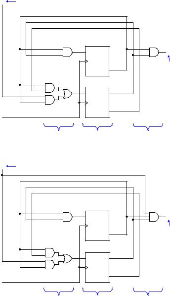
7.1Finite-State-Machine (FSM) Model
Figure 2 (a) shows the general schematic for the Moore FSM where its outputs are dependent only on its current state. Figure 2 (b) shows the general schematic for the Mealy FSM where its outputs are dependent on both the current state of the machine and also the inputs. In both figures, we see that the inputs to the next-state logic are the primary input signals and the current state of the machine. The next-state logic generates excitation values to change the state memory. The one difference in the two figures is that for the Moore FSM, the output logic only has the current state as its input, whereas, for the Mealy FSM, the output logic has both the current state and the input signals as its inputs.
Figure 2 (a) and (b) show a sample circuit of a Moore and Mealy FSM respectively. The two circuits are identical except for their outputs. For the Moore FSM, the output circuit is a 2-input AND gate that gets its input value from the outputs of the two D flip-flops. Remember that the state of the FSM is represented by the content of the state memory, which are the contents of the flip-flops. The content (or state) of a flip-flop is represented by the value at the Q (or Q' ) output. Hence, this circuit is only dependent on the current state of the machine.
Microprocessor Design – Principles and Practices with VHDL |
Last updated 7/18/2003 1:19 PM |

Chapter 7 − Sequential Circuits |
Page 3 of 36 |
For the Mealy FSM, the output circuit is a 3-input AND gate. In addition to getting its two inputs from the flipflops, the third input to this AND gate is connected to the primary input C. With this one extra connection, this output circuit is dependent on both the current state and the input.
For both circuits, the state memory consists of two D flip-flops. Having two flip-flops, four different combinations of values can be represented. Hence, this finite-state machine can be in any one of four different states. The state that this FSM will go to next depends on the value at the D inputs of the flip-flops.
Every flip-flop in the state memory requires a combinational circuit to generate a next-state value for its input(s). Since we have two D flip-flops, each having one input (D), therefore, the next-state logic circuit consists of two combinational circuits; one for input D0 and one for D1. The inputs to these two combinational circuits are the Q’s, which represent the current state of the flip-flops and the primary input C. Notice that it is not necessary for the input C to be an input to all the combinational circuits. In the sample circuit, only the bottom combinational circuit is dependent on the input C.
7.2Analysis of Sequential Circuits
Very often we are given a sequential circuit and need to know its operation. The analysis of sequential circuits is the process in which we are given a sequential circuit and we want to obtain a precise description of the operation of the circuit. The description of a sequential circuit can be in the form of a next-state / output table, or a state diagram. The steps for the analysis of sequential circuits are as follows:
1.Derive the excitation equations from the next-state logic circuit.
2.Derive the next-state equations by substituting the excitation equations into the flip-flop’s characteristic equations.
3.Derive the next-state table from the next-state equations.
4.Derive the output equations (if any) from the output logic circuit.
5.Derive the output table (if any) from the output equations.
6.Draw the state diagram from the next-state table and the output table.
|
|
|
|
Next-state |
|
|
|
State |
|
Output |
|
|
||
input signals |
|
|
|
|
|
|||||||||
|
|
|
|
Logic |
|
|
|
Memory |
current state |
Logic |
|
|
||
excitation |
|
output signals |
||||||||||||
|
|
|
|
Circuit |
Clock |
|
register |
|
|
|
Circuit |
|
|
|
|
|
|
|
|
|
|
|
|||||||
|
|
|
|
|
|
|
|
|
|
|
|
|
||
|
|
|
|
|
|
|
|
|
|
|
|
|
|
|
|
|
|
|
|
|
|
|
|
|
|
|
|
|
|
|
|
|
|
|
|
|
|
|
|
|
|
|
|
|
(a)
|
|
|
|
|
|
|
|
|
|
|
|
|
|
|
|
|
|
|
|
|
|
|
|
|
|
|
|
|
|
|
|
|
|
|
|
|
|
|
|
|
|
Output |
|
|
|
|
|
|
|
|
|
|
|
|
|
|
|
|
|
|
|
|
|
|
|
|
|
|
|
|
|
|
|
|
|
|
|
|
|
|
|
|
|
|
|
|
|
|
|
input signals |
|
Next-state |
|
|
State |
|
|
|
|
|
|
|||
|
|
|
|
Logic |
|
|
||||||||
|
|
|
|
Logic |
|
|
Memory |
|
|
|
|
|
|
|
|
|
|
|
excitation |
|
current state |
output signals |
|
||||||
|
|
|
|
|
Circuit |
|
||||||||
|
|
|
|
Circuit |
Clock |
|
register |
|
|
|
|
|
|
|
|
|
|
|
|
|
|
|
|
|
|
||||
|
|
|
|
|
|
|
|
|
|
|
||||
|
|
|
|
|
|
|
|
|
|
|
|
|
|
|
|
|
|
|
|
|
|
|
|
|
|
|
|
|
|
|
|
|
|
|
|
|
|
|
|
|
|
|
|
|
|
|
|
|
|
|
|
|
|
|
|
|
|
|
|
(b)
Figure 1. Finite-state machine models: (a) Moore FSM; (b) Mealy FSM.
Microprocessor Design – Principles and Practices with VHDL |
Last updated 7/18/2003 1:19 PM |
Chapter 7 − Sequential Circuits |
Page 4 of 36 |
C |
Input |
|
|
|
D1 |
Q1 |
Y |
|
Clk |
|
Output |
|
|
Q'1 |
|
|
D0 |
Q0 |
|
|
Clk |
|
|
Clk |
|
Q'0 |
|
|
|
|
Next-state logic State memory |
Output logic |
|
(a) |
|
|
C |
Input |
|
|
|
D1 |
Q1 |
Y |
|
Clk |
|
Output |
|
|
Q'1 |
|
|
D0 |
Q0 |
|
|
Clk |
|
|
Clk |
|
Q'0 |
|
|
|
|
Next-state logic State memory |
Output logic |
(b) Figure 2. Sample finite-state machine circuits: (a) Moore; (b) Mealy.
7.2.1 Excitation Equation
The excitation equations are the equations for the next-state logic circuit in the FSM. Since the next-state logic is a combinational circuit, therefore, deriving the excitation equations is just an analysis of a combinational circuit as discussed in Section 3.1.2. The next-state circuit that is derived by these equations “excites” the flip-flops by causing them to change states. These equations provide the signals to the inputs of the flip-flops, and are expressed as a function of the current state and the inputs to the FSM. The current state is determined by the current contents of the flip-flops, that is, the flip-flops’ output signal Q (and Q' ). There is one equation for each flip-flop’s input.
Microprocessor Design – Principles and Practices with VHDL |
Last updated 7/18/2003 1:19 PM |
Chapter 7 − Sequential Circuits |
Page 5 of 36 |
The following are two sample excitation equations for the two D flip-flops of Figure 2. The first equation provides the next-state circuit for the D input for flip-flop 1, and the second equation provides the circuit for the D input for flip-flop 0.
D1 |
= Q1'Q0 |
(1) |
D0 |
= Q1'Q0' + CQ1' |
(2) |
7.2.2 Next-state Equation
The next-state equations specify what the flip-flops’ next state is going to be depending on three things: 1) the current state of the flip-flops, 2) the functional behavior of the flip-flops, and 3) the inputs to the flip-flops. The current state of the flip-flops is just the Q outputs of the flip-flops. The functional behavior of a flip-flop, as you recall from Section 6.10.2, is described formally by its characteristic equation. The characteristic equation tells us
what Qnext ought to be, that is, what the next state ought to be. The inputs to the flip-flops are provided by the excitation equations as discussed in Section 7.2.1 above. Thus, to derive the next-state equations, we substitute the
excitation equations into the corresponding flip-flop’s characteristic equations. For example, the characteristic equation for the D flip-flop is
Qnext = D
Therefore, substituting the two excitation equations (1) and (2) from the previous sub-section into the characteristic equation for the D flip-flop will give us the following two next-state equations
Q1next = D1 |
= Q1'Q0 |
(3) |
Q0next = D0 |
= Q1'Q0' + CQ1' |
(4) |
7.2.3 Next-state Table
The next-state table is simply the truth table as derived from the next-state equations. It lists for every
combination of the current state (the Q) values and input values, what the next state (the Qnext) values should be. These next state values are obtained by substituting the current state and input values into the appropriate next-state
equations.
Figure 3 shows a sample next-state table with current states Q1Q0 equals to 00, 01, 10, and 11, and one input
signal C. The entries in the table are the next state values Q1next Q0next. These next state values are obtained from substituting the current state values Q1Q0 and input value C into the next-state equations (3) and (4) from Section
7.2.2 above.
For example, the top left entry tells us that if the current state is 00 and the input condition C = 0 is true then the next state that the FSM will go to is 01. Since 01 is also the next state from the current state 00 and the condition C = 1 is true, this means that the transition from state 00 to 01 does not depend on the input condition C, so this is an unconditional transition. From state 01, there are two conditional transitions: the FSM will transition to state 10 if the condition C = 0 is true, otherwise if C = 1, it will transition to state 11. Both states 10 and 11 go to state 00 unconditionally.
Current State |
Next State |
||
Q1next Q0next |
|||
Q1Q0 |
|||
C = 0 |
C = 1 |
||
|
|||
00 |
01 |
01 |
|
01 |
10 |
11 |
|
10 |
00 |
00 |
|
11 |
00 |
00 |
|
Figure 3. A next-state table with four states and one input signal C.
Microprocessor Design – Principles and Practices with VHDL |
Last updated 7/18/2003 1:19 PM |
Chapter 7 − Sequential Circuits |
Page 6 of 36 |
7.2.4 Output Equation
The output equations are the equations derived from the combinational output logic circuit in the FSM. Depending on the type of FSM (Moore or Mealy), the output equations can be dependent on just the current state or on both the current state and the inputs.
For the Moore circuit of Figure 2 (a), the output equation is |
|
Y = Q1'Q0 |
(5) |
For the Mealy circuit of Figure 2 (b), the output equation is |
|
Y = CQ1'Q0 |
(6) |
A typical FSM will have many output signals, and so there will be one equation for every output signal. |
|
7.2.5 Output Table
Like the next-state table, the output table is the truth table that is derived from the output equations. The output tables for the Moore and Mealy FSMs are slightly different from each other. For the Moore FSM, the output table lists for every combination of the current state what the output values should be. Whereas for the Mealy FSM, the output table lists for every combination of the current state and input values what the output values should be. These output values are obtained by substituting the current state and input values into the appropriate output equations.
Figure 4 (a) and (b) show sample output tables for the Moore and Mealy FSMs as derived from the output equations (5) and (6) respectively from Section 7.2.4 above. For the Moore FSM, the output signal Y is dependent only on the current state value Q1Q0, whereas, for the Mealy FSM, the output signal Y is dependent on both the current state and input C.
Current State |
Output |
|
Current State |
Output |
||
|
|
Y |
||||
Q1Q0 |
Y |
|
Q1Q0 |
|
||
|
C = 0 |
|
C = 1 |
|||
|
|
|
|
|
||
00 |
0 |
|
00 |
0 |
|
0 |
01 |
1 |
|
01 |
0 |
|
1 |
10 |
0 |
|
10 |
0 |
|
0 |
11 |
0 |
|
11 |
0 |
|
0 |
(a) |
|
|
|
(b) |
|
|
Figure 4. Output table: (a) for Moore FSM; (b) for Mealy FSM.
7.2.6 State Diagram
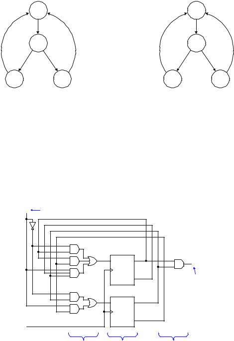
A state diagram is a graph with nodes and directed edges connecting the nodes. The state diagram graphically portraits the operation of the FSM. There is one node for every state of the FSM and these nodes are labeled with the state in which they represent. For every state transition of the FSM there is a directed edge connecting two nodes. The directed edge originates from the node that represents the current state that the FSM is transitioning from, and goes to the node that represents the next state that the FSM is transitioning to. Edges may or may not have labels on them. Edges for unconditional transitions from one state to another will not have a label. In this case, only one edge can originate from that node. Conditional transitions from a state will have two outgoing edges. The two edges from this state have the corresponding input signal conditions labeled on them – one edge with the label for when the condition is true and the other edge with the label for when the condition is false.
Figure 5 (a) shows a small state diagram with four states, 00, 01, 10, and 11, and one input signal C. This state diagram is derived from the next-state table shown in Figure 3 and the output table from Figure 4 (a). There are three unconditional transitions, 00 to 01, 10 to 00, and 11 to 00, and one conditional transition from 01 to 10 or 11. For the conditional transition from 01, if the condition C = 0 is true then the transition from 01 to 10 is made. Otherwise, if the condition C = 0 is false, that is C = 1 is true, then the transition from 01 to 11 is made.
Microprocessor Design – Principles and Practices with VHDL |
Last updated 7/18/2003 1:19 PM |
Chapter 7 − Sequential Circuits |
Page 7 of 36 |
The output signal Y in Figure 5 (a) is labeled inside each node denoting that the output is dependent only on the current state. For example, when the FSM is in state 01, the output Y is 1, whereas, in state 11, Y is 0. Hence, this state diagram is for the Moore FSM.
In Figure 5 (b), the output signal Y is labeled on the edges denoting that the output is dependent on both the current state and the input signal C. For example, when the FSM is in state 01, if the FSM takes the left edge for C = 0 to state 10, then it will output a 0 for Y. However, if the FSM takes the right edge for C = 1 to state 11, then it will output a 1 for Y. Hence, this state diagram is for the Mealy FSM.
|
00 |
|
00 |
|
|
Y = 0 |
|
||
|
|
|
||
|
|
Y = 0 |
||
|
01 |
Y = 0 |
Y = 0 |
|
|
|
01 |
||
|
Y = 1 |
|
||
|
|
|
||
C = 0 |
C = 1 |
C = 0 |
C = 1 |
|
Y = 0 |
Y = 1 |
|||
|
|
|||
10 |
11 |
10 |
11 |
|
Y = 0 |
Y = 0 |
|||
|
|
|||
|
(a) |
|
(b) |
|
Figure 5. A state diagram with four states and one input signal: (a) Moore FSM using actual state encodings; (c) Mealy FSM using actual state encodings.
7.2.7 Example: Analysis of a Moore FSM
We will now illustrate the complete process of analyzing a Moore FSM with an example.
Example 7.1
Figure 6 shows a simple sequential circuit. Comparing this circuit with the general FSM schematic in Figure 1, we conclude that this is a Moore type FSM since the output logic consists of a 2-input AND gate that is dependent only on the current state Q1Q0. We will follow the above six steps to do a detail analysis of this circuit.
C |
Input |
|
|
|
D1 |
Q1 |
Y |
|
Clk |
|
|
|
|
Output |
|
|
|
Q'1 |
|
|
|
|
|
|
D0 |
Q0 |
|
|
Clk |
|
|
|
|
Q'0 |
|
Clk
Next-state logic State memory |
Output logic |
Figure 6. A simple Moore finite-state machine.
Microprocessor Design – Principles and Practices with VHDL |
Last updated 7/18/2003 1:19 PM |
Chapter 7 − Sequential Circuits |
Page 8 of 36 |
Step 1 is to derive the excitation equations, which are the equations for the next-state logic circuit. These equations are dependent on the current state of the flip-flops Q1 and Q0, and the input C. One equation is needed for every data input of all the flip-flops in the state memory. Our sample circuit has two flip-flops having the two inputs D1, and D0, so we get the two excitation equations as shown in Figure 7 (a). These two equations are obtained from analyzing the two combinational circuits that provide the inputs D1 and D0 to the two flip-flops. For this particular example, both of these combinational circuits are simple two level sum-of-products circuits.
Step 2 is to derive the next-state equations. These equations tell us what the next-state is going to be given the current state of the state memory, the functional behavior of the flip-flops and the inputs to the flip-flops. One equation is needed for every flip-flop. The functional behavior of the flip-flop is described by its characteristic
equation, which for the D flip-flop, is Qnext = D. The inputs to the flip-flops are just the excitation equations derived from step 1. Hence, we simply substitute the excitation equation into the characteristic equation for each flip-flop to
obtain the next-state equation for that flip-flop. With two flip-flops in the example, we get two next-state equations, one for Q1next and one for Q0next. Figure 7 (b) shows these two next-state equations.
Step 3 is to derive the next-state table. The next-state values in the table are obtained by substituting every combination of current state and input values into the next-state equations obtained in step 2. In our example, there are two flip-flops, Q1 and Q0, and input C. Hence the table will have eight next-state entries. There are two bits for every entry – the first bit for Q1next, and the second for Q0next.
D1 = C'Q1 + Q1Q0' + CQ1'Q0
D0 = C'Q0 + CQ0'
|
|
(a) |
|
|
Q1next = D1 = C'Q1 + Q1Q0' + CQ1'Q0 |
|
|||
Q0next = D0 = C'Q0 + CQ0' |
|
|
||
|
|
(b) |
|
|
|
Current State |
Next State |
||
|
Q1next |
Q0next |
||
|
Q1Q0 |
|
||
|
C = 0 |
C = 1 |
||
|
|
|||
|
00 |
|
00 |
01 |
|
01 |
|
01 |
10 |
|
10 |
|
10 |
11 |
|
11 |
|
11 |
00 |
|
|
(c) |
|
|
C = 0 |
Q 1 Q 0 = 00 |
C = 1 |
Q 1 Q 0 = 01 |
|
|
Y = 0 |
|
|
Y = 0 |
|
C = 1 |
|
|
C = 1 |
C = 0 |
Q 1 Q 0 = 11 |
|
Q |
1 Q 0 = 10 |
|
Y = 1 |
C = 1 |
Y = 0 |
|
(f)
Y = Q1Q0
(d)
Current State |
Output |
Q1Q0 |
Y |
00 |
0 |
01 |
0 |
10 |
0 |
11 |
1 |
(e)
C = 0 |
Clk |
|
|
|
|
|
|
|
|
|
|
|
|
|
|
|
|
|
|
|
|
|
|
|
|
|
|
|
|
|
|
|
|
|
|
C |
|
|
|
|
|
|
|
|
|
|
|
|
|
||||
|
|
|
|
|
|
|
|
|
|
|
|
|
|
||||
|
|
|
|
|
|
|
|
|
|
|
|
|
|
||||
|
Q |
1 |
|
|
|
|
|
|
|
|
|
|
|
|
|
|
|
|
|
|
|
|
|
|
|
|
|
|
|
|
|
|
|
||
C = 0 |
Q0 |
|
|
|
|
|
|
|
|
|
|
|
|
|
|||
|
|
|
|
|
|
|
|
|
|
|
|
|
|||||
Y |
|
|
|
|
|
|
|
|
|
|
|
|
|
||||
|
|
|
|
|
|
|
|
|
|
|
|
|
|||||
|
|
|
|
|
|
|
|
|
|
|
|
|
|
|
|
|
|
t0 |
t1 t2 |
t3 |
t4 |
t5 |
t6 t7 |
(g)
Figure 7. Analysis of a Moore FSM: (a) excitation equations; (b) next-state equations; (c) next-state table; (d) output equation; (e) output table; (f) state diagram; (g) timing diagram.
Microprocessor Design – Principles and Practices with VHDL |
Last updated 7/18/2003 1:19 PM |
Chapter 7 − Sequential Circuits |
Page 9 of 36 |
For example, to find the Q1next value for the current state Q1Q0 = 00 and C = 1 (the blue entry), we substitute the
values Q1 = 0, Q0 = 0 and C = 1 into the equation Q1next = C'Q1 + Q1Q0' + CQ1'Q0 = (1' • 0) + (0 • 0' ) + (1 • 0' • 0) to get the value 0. Similarly, we get Q0next by substituting the same values for Q1, Q0, and C into the equation Q0next =
C'Q0 + CQ0' = (1' • 0) + (1 • 0' ) to get the value 1. The resulting next-state table for our example is shown in Figure 7 (c).
Step 4 is to derive the output equations from the output logic circuit. One output equation is needed for every output signal. For our example, there is only one output signal Y that is dependent only on the current state of the machine. The output equation for Y as derived from the sample circuit diagram is shown in Figure 7 (d).
Step 5 is to derive the output table. Just like the next-state table, the output table is obtained by substituting all possible combinations of the current state values into the output equation(s) for the Moore FSM. The output table for our Moore FSM example is shown in Figure 7 (e).
Step 6 is to draw the state diagram, which is derived directly from the next-state and output tables. Every state in the next-state table will have a corresponding node labeled with the state encoding in the state diagram. For every next state entry in the next-state table, there will be a corresponding directed edge. This edge originates from the node labeled with the current state and ends at the node labeled with the next state entry. The edge is labeled with the corresponding input conditions.
For example, in the next-state table, when the current state Q1Q0 is 00, the next state Q1next Q0next is 01 for the input C = 1. Hence, in the state diagram, there is a directed edge from node 00 to node 01 with the label C = 1. For a
Moore FSM, the outputs are dependent only on the current state, thus the output values from the output table are included inside each node of the state diagram. The complete state diagram for our example is shown in Figure 7 (f).
A sample timing diagram for the execution of the circuit is shown in Figure 7 (g). The two D flip-flops used in the circuit are positive edge-triggered flip-flops so they change their states at each rising clock edge. Initially, we assume that these two flip-flops are both in state 0. The first rising clock edge is at time t0. Normally, the flip-flops will change state at this time, however, since C is a 0, the flip-flops’ values remain constant. At time t1, C changes to a 1, so that at the next rising clock edge at time t2, the flip-flop values Q1Q0 changes to 01. At the next two rising clock edges, t3 and t4, the value for Q1Q0 changes to 10, then 11 respectively. At time t4 when Q1Q0 = 11, the output Y also changes to a 1 since Y = Q1 • Q0. At time t5, input C drops back down to a 0 but the output Y remains at a 1. Q1Q0 remains the same at 11 through the next rising clock edge since C is 0. At time t6, C changes back to a 1 and so at the next rising clock edge at time t7, Q1Q0 increments again to 00 and the cycle repeats.
When C = 1, the FSM cycles through the four states in order repeatedly. When C = 0, the FSM stops at the current state until C is asserted again. If we interpret the four state encodings as a decimal number, then we can conclude that the circuit of Figure 6 is for a modulo-4 up counter that cycles through the four values 0, 1, 2, and 3. The input C enables or disables the counting. ♦
7.2.8 Example: Analysis of a Mealy FSM
Example 7.2 illustrates the process for performing an analysis on a Mealy FSM.
Example 7.2
Figure 8 shows a simple Mealy FSM. This circuit is exactly like the one in Figure 6 except that the output circuit, which in this example is just one 3-input AND gate, is dependent on not only the current state Q1Q0, but also on the input C.
The analysis for this circuit goes exactly like the one for the Moore FSM in Example 7.1 up to creating the nextstate table in step 3. The only difference is in deriving the output equation and output table for steps 4 and 5. For a Mealy FSM, the output equation is dependent on both the current state and the input value. Since the circuit has only one output signal, we obtain the output equation that is dependent on C as shown in Figure 9 (a). Figure 9 (b) shows the resulting output table obtained by substituting all possible values for Q1, Q0, and C into the output equation.
For the state diagram, we cannot put the output value inside a node since the output value is dependent on the current state and the input value. Thus, the output value is placed on the edge that corresponds to the current state value and input value as shown in Figure 9 (c). Output signal Y is 0 for all edges except for the one originating from state 11 having the input condition C = 1. On this one edge, Y is a 1.
Microprocessor Design – Principles and Practices with VHDL |
Last updated 7/18/2003 1:19 PM |

Chapter 7 − Sequential Circuits |
Page 10 of 36 |
A sample timing diagram is shown in Figure 9 (d). This diagram is exactly the same as the one for the Moore FSM shown in Figure 7 (g) up to time t5. At time t5, input C drops to a 0, and so output Y also drops to a 0 since Y = C • Q1 • Q0. At time t6, C rises back up to a 1, and so Y also rises to a 1 immediately. Since the output circuit is a combinational circuit, Y does not change at the active edge of the clock, but changes immediately when the inputs change. At time t7 when Q1Q0 changes to 00, Y again changes back to a 0.
Except for the difference in how this circuit generates the output signal Y, this Mealy FSM behaves exactly the same as the Moore FSM from Example 7.1 in the way that it changes from one state to the next. This, of course, is due to the fact that both next-state tables are identical. Thus, this Mealy FSM circuit is also a modulo-4 up counter.♦
C |
Input |
|
|
|
|
|
D1 |
Q1 |
Y |
|
|
Clk |
|
Output |
|
|
|
Q'1 |
|
|
|
D0 |
Q0 |
|
|
|
Clk |
|
|
Clk |
|
|
Q'0 |
|
|
|
|
|
|
|
Next-state logic |
State memory |
Output logic |
|
Figure 8. A simple Mealy finite-state machine.
Y= CQ1Q0
(a)
Current State |
Output |
||
|
Y |
||
Q1Q0 |
|
||
C = 0 |
|
C = 1 |
|
|
|
||
00 |
0 |
|
0 |
01 |
0 |
|
0 |
10 |
0 |
|
0 |
11 |
0 |
|
1 |
(b)
Microprocessor Design – Principles and Practices with VHDL |
Last updated 7/18/2003 1:19 PM |