

08.Noise
.pdf164 NOISE
Replacing the power levels in Eq. (8.98) with their explicit expression gives the value for the overall efficiency of a chain of unilateral amplifiers:
, |
|
|
|
|
|
|
|
G1G2G3 . . . Gn 1 |
|
|
8.99 |
||
T D G1 |
1 G1 |
G2 |
|
G1G2 . . . Gn 1 Gn 1 |
|||||||||
|
1 |
|
|
||||||||||
|
|
,1 |
C |
|
,2 |
|
C Ð Ð Ð C |
|
,n |
|
|
||
When each amplifier stage has a gain sufficiently greater than one, the overall efficiency becomes
,T ³ |
|
1 |
|
8.100 |
1 |
1 |
1 |
C Ð Ð Ð C C
G2G3 . . . Gn,1 Gn,n 1 ,n
This final equation illustrates that it is important to make the final stage the most efficient one
8.11AMPLIFIER DESIGN FOR OPTIMUM GAIN AND NOISE
The gain for a nonunilateral amplifier was previously given as Eq. (7.15) is repeated here:
G |
|
jS21j2 1 j Gj2 1 j Lj2 |
8.101 |
|
T D j 1 GS11 1 LS22 S12S21 G Lj2 |
||||
|
|
|||
If S12 is set to zero, thereby invoking the unilateral approximation for the amplifier gain, then
G |
|
1 j Gj2 |
S |
21j |
2 |
1 j Lj2 |
8.102 |
|
|
|
j 1 LS22j2 |
||||
|
T ³ j1 GS11j2 j |
|
|
||||
This approximation of course removes the possibility of analytically determining the transistor stability conditions. Using this expression, a set of constant gain circles can be drawn on a Smith chart for a given transistor. That is, for a given set of device scattering parameters and for a fixed load impedance, a set of constant gain circles can be drawn for a range of generator impedances expressed here in terms of G.
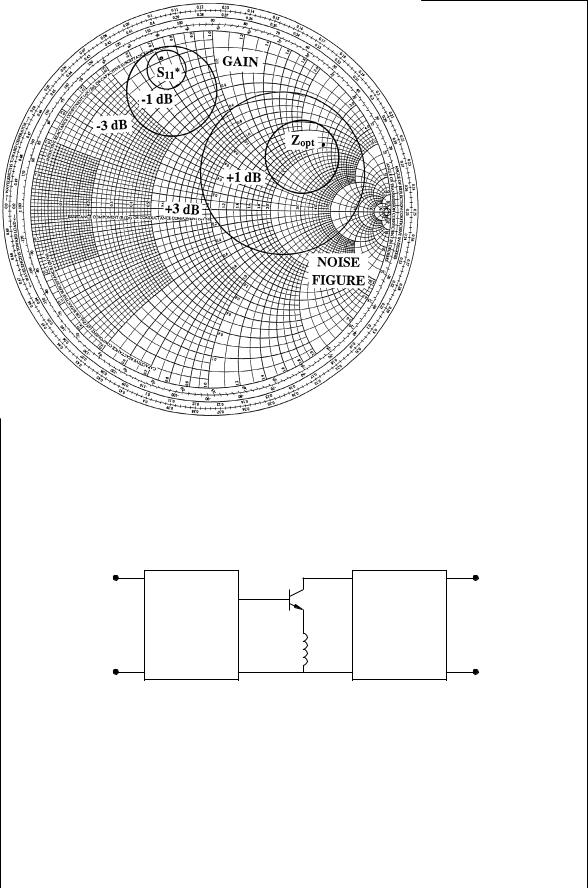
The noise figure was previously found in Eq. (8.40). As was done for the constant gain circles, constant noise figure circles can be drawn for a range of values for the generator admittance, YG D GG C jBG. The optimum gain occurs when G D S11Ł , and the minimum noise figure occurs when YG D Yopt. These two source impedances are rarely the same, but a procedure is available that at least optimizes both of these parameters simultaneously [15]. As seen on the Smith chart in Fig. 8.9, it appears that the least damage to either the gain or the noise figure is obtained if the actual chosen generator impedance lies on a
AMPLIFIER DESIGN FOR OPTIMUM GAIN AND NOISE |
165 |
FIGURE 8.9 Constant gain and noise figure circles.
Input |
Output |
Match |
Match |
Circuit |
Circuit |
FIGURE 8.10 Series inductive feedback can be used to lower noise figure.
line between S11Ł and Yopt. It has been found that addition of series inductance, such as shown in Fig. 8.10, will lower the minimum noise figure of the circuit because it lowers the effective Fmin and rn. This series inductance also increases the real part of the input impedance. The output impedance does not affect the noise figure, but it can be manipulated to adjust the gain.
166 NOISE
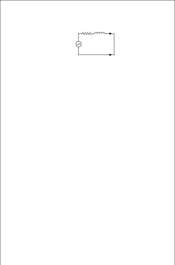
R L
+
< v 2 >
–
FIGURE 8.11 Noise current developed by a series RL circuit.
PROBLEMS
8.1What is the noise voltage at the output of Fig. 8.2 when the capacitor is removed from the circuit?
8.2What is the noise current from a noise voltage source in a series RL circuit shown in Fig. 8.11.
8.3Derive Eqs. (8.80) to (8.83).
8.4 A MESFET has a base width W D 300 m and at 2 GHz with a given bias is found to have gm D 75 mS, Rg D 1 -, Rd D 5 -, Rs D 3 -, and Cgs D 0.4 pF. What are the four noise parameters Fmin, Rn, Ropt, and Xopt? If the base width is changed to W0 D 200 m and the number of base fingers remains unchanged, what are the four noise parameters?
8.5A three-stage amplifier consists of three individual unilateral amplifiers. The first one (the input stage) has a gain G1 D 10 dB, a noise figure F1 D 1.5, and an efficiency ,1 D 1%. For stage 2, G2 D 20 dB, F2 D 10, and ,2 D 5%. For stage 3, G3 D 5 dB, F3 D 15, and ,3 D 50%. What is the overall total noise figure for the cascaded amplifier? What is the overall total efficiency for the cascaded amplifier?
REFERENCES
1.J. L. Plumb and E. R. Chenette, “Flicker Noise in Transistors,” IEEE Trans. Electron Devices, Vol. 10, pp. 304–308, 1963.
2.A. Messiah, Quantum Mechanics, Amsterdam: North-Holland 1964, ch. 12.
3.W. A. Davis, Microwave Semiconductor Circuit Design, New York: Van Nostrand, 1984, chs. 8, 9.
4.A. E. Siegman, “Zero-Point Energy as the Source of Amplifier Noise,” Proc. IRE, Vol. 49, pp. 633–634, 1961.
5.H. Nyquist, “Thermal Agitation of Electronic Charge in Conductors,” Physical Rev., Vol. 32, p. 110, 1928.
6.K. Kurokawa, “Actual Noise Measure of Linear Amplifiers,” Proc. IRE, Vol. 49, pp. 1391–1397, 1961.
7.H. A. Haus, “IRE Standards on Methods of Measuring Noise in Linear Twoports,” Proc. IRE, Vol. 47, pp. 66–68, 1959.

REFERENCES 167
8. H. Rohte and W. Danlke, “Theory of Noisy Fourpoles,” Proc. IRE, Vol. 44,
pp. 811–818, 1956.
9.H. A. Haus, “Representation of Noise in Linear Twoports,” Proc. IRE, Vol. 48,
pp. 69–74, 1960.
10.H. Fukui, “Design of Microwave GaAs MESFETs for Broad-Band Low-Noise Amplifiers,” IEEE Trans. Electron Devices, Vol. 26, pp. 1032–1037, 1979.
11.J. M. Golio, Microwave MESFETs and HEMTs, Norwood, MA: Artech House, 1991, ch. 2.
12.H. Fukui, “The Noise Performance of Microwave Transistors,” IEEE Trans. Electron Devices, Vol. 13, pp. 329–341, 1966.
13.R. J. Hawkins, “Limitations of Nielsen’s and Related Noise Equations Applied to Microwave Bipolar Transistors, and a New Expression for the Frequency and Current Dependent Noise Figure,” Solid State Electronics, Vol. 20, pp. 191–196, 1977.
14.H. T. Friis, “Noise Figures of Radio Receivers,” Proc. IRE, Vol. 32, pp. 419–422, 1944.
15.R. E. Lehmann and D. D. Heston, “X-Band Monolithic Series Feedback LNA,” IEEE Trans. Microwave Theory Tech., Vol. 33, pp. 1560–1566, 1985.