

10.Oscillators and harmonic generators
.pdfRadio Frequency Circuit Design. W. Alan Davis, Krishna Agarwal
Copyright 2001 John Wiley & Sons, Inc.
Print ISBN 0-471-35052-4 Electronic ISBN 0-471-20068-9
CHAPTER TEN
Oscillators and Harmonic
Generators
10.1OSCILLATOR FUNDAMENTALS
An oscillator is a circuit that converts energy from a power source (usually a dc power source) to ac energy. In order to produce a self-sustaining oscillation, there necessarily must be feedback from the output to the input, sufficient gain to overcome losses in the feedback path, and a resonator. There are number of ways to classify oscillator circuits, one of those being the distinction between one-port and two-port oscillators. The one-port oscillator has a load and resonator with a negative resistance at the same port, while the two-port oscillator is loaded in some way at the two ports. In either case there must be a feedback path, although, in the case of the one-port, this path might be internal to the device itself.
An amplifier with positive feedback is shown in Fig. 10.1. The output voltage of this amplifier is
Vo D aVi C aˇVo
which gives the closed loop gain |
|
|
|
|
A D |
Vo |
D |
a |
10.1 |
Vi |
1 aˇ |
|||
The positive feedback allows an increasing output voltage to feedback to the input side until the point is reached where
aˇ D 1 |
10.2 |
This is called the Barkhausen criterion for oscillation and is often described in terms of its magnitude and phase separately. Hence oscillation can occur
195

196 OSCILLATORS AND HARMONIC GENERATORS
Vi |
+ + |
a |
Vo |
 +
+
β
FIGURE 10.1 Circuit with positive feedback.
+
Vi
–
Ii
+
Vi
–
Ii
Na
Nf
Na
Nf
Na
Nf
Na
Nf
|
|
|
|
Io |
[Z ] |
Io |
||||
|
|
|
|
|||||||
|
|
|
|
|
|
|
|
|||
|
|
|
|
|
|
|
|
|||
|
|
|
|
|
|
|
|
A = |
||
|
|
|
|
|
|
|
|
Vi |
||
|
|
|
|
|
|
|
|
|
|
|
|
|
|
|
|
|
|
|
|
|
|
|
|
|
|
|
|
|
|
|
|
|
|
|
|
|
|
|
|
|
|
|
|
|
+ |
|
|
|
|
|
|
|||
|
|
Vo |
[Y ] |
Vo |
||||||
|
|
|||||||||
|
|
|||||||||
|
|
A = |
||||||||
|
|
– |
Ii |
|
||||||
|
|
|||||||||
|
|
|
|
|
||||||
|
|
|
|
|
|
|
|
|
|
|
|
|
|
|
|
|
|
|
|
|
|
|
|
|
|
|
|
|
|
|
|
|
|
+ |
|
|
|
|
|
|
|||
|
|
Vo |
[H ] |
Vo |
|
|||||
|
|
|||||||||
|
|
A = |
||||||||
|
|
– |
Vi |
|||||||
|
|
|
|
|
||||||
|
|
|
Io |
[G ] |
Io |
|
||||
|
|
|
||||||||
|
|
|
||||||||
|
|
|
|
|
|
|
|
|||
|
|
|
|
|
|
|
|
|||
|
|
|
|
|
|
|
|
|||
|
|
|
|
|
|
|
|
A = |
||
|
|
|
|
|
|
|
|
Ii |
||
|
|
|
|
|
|
|
|
|
|
|
|
|
|
|
|
|
|
|
|
|
|
FIGURE 10.2 Four possible ways to connect the amplifier and feedback circuit. The composite circuit is obtained by adding the designated two-port parameters. The units for “gain” are as shown.

TWO-PORT OSCILLATORS WITH EXTERNAL FEEDBACK |
197 |
when jaˇj D 1 and 6aˇ D 360°. An alternate way of determining conditions for oscillation is determining when the value k < 1 for the stability circle as described in Chapter 7. Still a third way will be considered later in Section 10.4.
10.2FEEDBACK THEORY
The active amplifier part and the passive feedback part of the oscillator can be considered as a pair of two two-port circuits. Usually the connection of these two-ports occurs in four different ways: series–series, shunt–shunt, series–shunt, and shunt–series (Fig. 10.2). A linear analysis of the combination of these two two-ports begins by determining what type of connection exists between them. If, for example, they are connected in series–series, then the best way to describe each of the two-ports is in terms of their z parameters. A description of the composite of the two two-ports is found by simply adding the z parameters of the two circuits together. Thus, if [za] and [zf] represent the amplifier and feedback circuits connected in series–series, then the composite circuit is described by [zc] D [za] C [zf]. The form of the feedback circuit itself can take a wide range of forms, but being a linear circuit, it can always be reduced to a set of z, y, h or g parameters, any one of which can be represented by k for the present. The term that feeds back to the input of the amplifier is k12f. The k12f term, though small, is a significant part of the small incoming signal, so it cannot be neglected. The open loop gain, a, of the composite circuit is found by setting k12f D 0. Then, using the normal circuit analysis, the open loop gain is determined. The closed loop gain is found by including k12f in the closed loop gain given by Eq. (10.1). The Barkhausen criterion for oscillation is satisfied when ak12f D aˇ D 1.
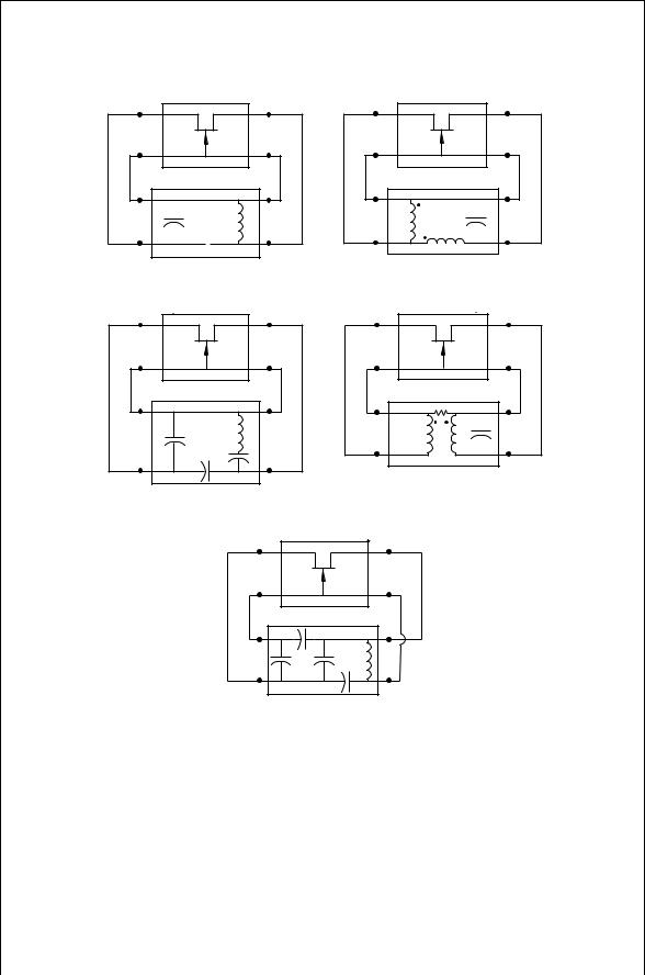
10.3TWO-PORT OSCILLATORS WITH EXTERNAL FEEDBACK
There are a wide variety of two-port oscillator circuits that can be designed. The variety of oscillators results from the different ways the feedback circuit is connected to the amplifier and the variety of feedback circuits themselves. Five of these shown in Fig. 10.3 are known as the Colpitts, Hartley, ClappGouriet [1,2], Armstrong, and Vackar [2,3] oscillators. The Pierce oscillator is obtained by replacing the inductor in the Colpitts circuit with a crystal that acts like a high Q inductor. As shown the first four of these feedback circuits are drawn in a series–series connection, while the Vackar is drawn as a series–shunt configuration. Of course a wide variety of connections and feedback circuits are possible. In each of these oscillators, there is a relatively large amount of energy stored in the resonant reactive circuit. If not too much is dissipated in the load, sustained oscillations are possible.
The Colpitts is generally favored over that of the Hartley, because the Colpitts circuit capacitors usually have higher Q than inductors at RF frequencies and come in a wider selection of types and sizes. In addition the inductances in the Hartley circuit can provide a means to generate spurious frequencies because it
198 OSCILLATORS AND HARMONIC GENERATORS
C 2 L C1 
L 2 |
L1 |
C |
|
(a ) |
(b ) |
|
|
L |
C1 |
C2 |
C 3 |
(c )
C
L1 |
L2 |
|
|
|
(d ) |
C x |
C v |
L |
|
|
C1 |
C 2 |
|
|
|
|
(e ) |
|
|
|
FIGURE 10.3 Oscillator types: (a) |
Colpitts, |
(b) Hartley, (c) Clapp-Gouriet, (d) |
||
Armstrong, and (e) Vackar. |
|
|
|
|
is possible to resonate the inductors with parasitic device capacitances. Because the first element in the Colpitts circuit is a shunt capacitor, it can be said to be a low-pass circuit. For similar reasons the Hartley is a high-pass circuit and the Clapp-Gouriet is a bandpass circuit. There is an improvement in the frequency stability of the tapped capacitor circuit over that of a single LC tuned circuit [1].

TWO-PORT OSCILLATORS WITH EXTERNAL FEEDBACK |
199 |
In a voltage-controlled oscillator application, it is often convenient to vary the capacitance to change the frequency. This can be done using a reverse biased varactor diode as the capacitor. If the capacitance shown in Fig. 10.4a changes because of say a temperature shift, the frequency will change by
df |
dC0 |
10.3 |
|
|
D |
|
|
|
|
||
f2C0
However, the tapped circuit in Fig. 10.4b in which C2 is used for tuning a Colpitts circuit has a frequency stability given by
df |
D |
C0 |
|
dC2 |
10.4 |
|
f |
C2 C2 |
|||||
|
|
|||||
This has an improved stability by the factor of C0/C2. Furthermore, by increasing C0 so that C1 and C2 are increased by even more while adjusting the inductance to maintain the same resonant frequency, the stability can be further enhanced. The Clapp-Gouriet circuit exhibits even better stability than the Colpitts [2]. In this circuit, C1 and C2 are chosen to have large values compared to the tuning capacitor C3. The minimum transistor transconductance, gm, required for oscillation for the Clapp-Gouriet circuit increases / ω3/Q. While the Q of a circuit often rises with frequency, it would not be sufficient to overcome the cubic change in frequency. For the Vackar circuit, the required minimum gm to maintain oscillation is / ω/Q. This would tend to provide a slow drop in the amplitude of the oscillations as the frequency rises [2].
The oscillator is clearly a nonlinear circuit, but nonlinear circuits are difficult to treat analytically. In the interest of trying to get a design solution, linear analysis is used. It can be said that a circuit can be treated by small signal linear mathematics to just prior to it’s breaking into oscillation. In going through the transition between oscillation and linear gain, the active part of the circuit does not change appreciably. As a justification for using linear analysis, the previous statement certainly has some flaws. Nevertheless, linear analysis does give remarkably close answers. More advanced computer modeling using methods like harmonic balance will give more accurate results and provide predictions of output power.
L |
|
C2 |
C0 |
L |
|
|
|
C1 |
|
(a ) |
(b ) |
FIGURE 10.4 (a) Simple LC resonant circuit and (b) tapped capacitor LC circuit used in the Colpitts oscillator.

200 OSCILLATORS AND HARMONIC GENERATORS
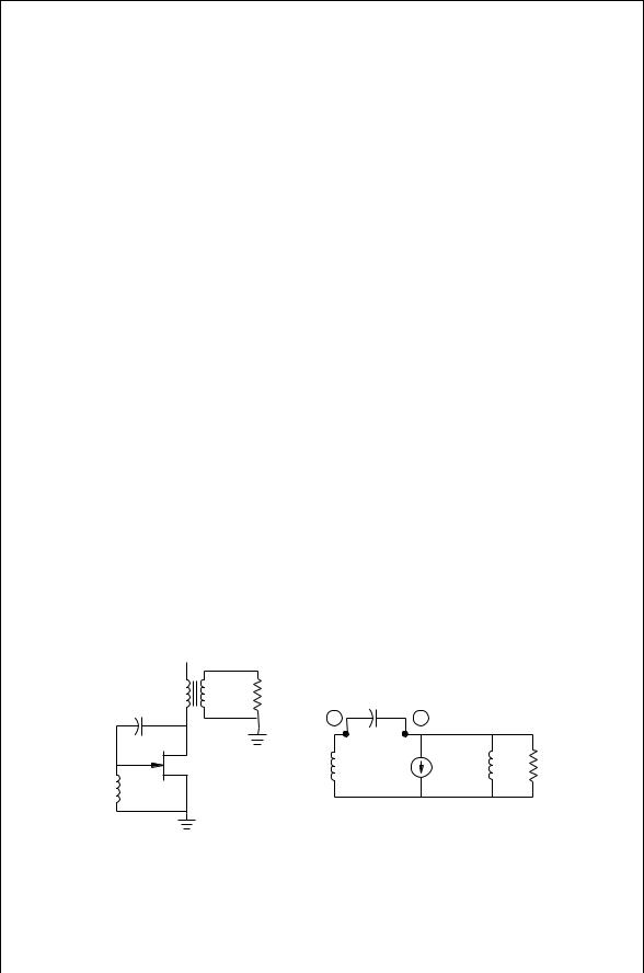
As an example, consider the Colpitts oscillator in Fig. 10.5. Rather than drawing it as shown in Fig. 10.3a as a series–series connection, it can be drawn in a shunt–shunt connection by simply rotating the feedback circuit 180° about its x-axis. The y parameters for the feedback part are
y11f |
D sC1 |
1 |
10.5 |
||||
C |
|
||||||
sL |
|||||||
y22f |
D sC2 |
1 |
10.6 |
||||
C |
|
||||||
sL |
|||||||
y |
|
|
1 |
|
|
|
10.7 |
12f |
D sL |
|
|
||||
|
|
|
|
||||
The equivalent circuit for the y parameters now may be combined with the equivalent circuit for the active device (Fig. 10.6). The open loop gain, a, is found by setting y12f D 0.
vo |
|
gm C y12f |
10.8 |
|
vgs |
D 1/RD C y22f |
|||
|
||||
In the usual feedback amplifier theory described in electronics texts, the y21f term would be considered negligible, since the forward gain of the feedback circuit would be very small compared to the amplifier. This cannot be assumed here.
R D
C 1 L
C 2
FIGURE 10.5 Colpitts oscillator as a shunt–shunt connection.
+ |
|
|
|
|
+ |
Vgs y 11f |
y 12fV o |
gmV gs |
y 21fVgs |
y 22f |
1 / R D Vo |
– |
|
|
|
|
– |
FIGURE 10.6 Equivalent circuit of the Colpitts oscillator.

TWO-PORT OSCILLATORS WITH EXTERNAL FEEDBACK |
201 |
The open loop gain, a, for the shunt–shunt configuration is
a |
|
vo |
|
vo |
|
gm C y12f |
10.9 |
|
D ii |
D vgsy11f |
D y11f[ 1/RD C y22f] |
||||||
|
|
|||||||
The negative sign introduced in getting ii is needed to make the current go north rather than south as made necessary by the usual sign convention. Finally, by the Barkhausen criterion, oscillation occurs when ˇa D 1:
1 |
D |
ay |
|
y12f gm C y12f |
10.10 |
|
12f D y11f[ 1/RD C y22f] |
||||||
|
|
|
||||
Making the appropriate substitutions from Eqs. (10.5) through (10.7) results in the following:
|
gm sL D sL sC1 |
C sL R1D |
C sC1 |
C sL sC2 |
C sL |
10.11 |
|||||
|
1 |
|
1 |
|
|
|
1 |
|
1 |
|
|
Both the real and imaginary parts of this equation must be equal on both sides. Since s D jω0 at the oscillation frequency, all even powers of s are real and all odd powers of s are imaginary. Since gm in Eq. (10.11) is associated with the real part of the equation, the imaginary part should be considered first:
sL D sL s2C1C2 C |
L1 |
C |
L2 |
C s2L2 |
10.12 |
||
1 |
|
C |
|
C |
1 |
|
|
When this is solved, the oscillation frequency is found to be
0 |
D |
|
|
LC1C2 |
|
|
ω |
|
|
|
C1 C C2 |
|
10.13 |
|
|
|
|
|||
Solving the real part of Eq. (10.11) with the now known value for ω0 gives the required value for gm:
C1 |
10.14 |
gm D RDC2 |
The value for gm found in Eq. (10.14) is the minimum transconductance the transistor must have in order to produce oscillations. The small signal analysis is sufficient to determine conditions for oscillation assuming the frequency of oscillation does not change with current amplitude in the active device. The large signal nonlinear analysis would be required to determine the precise frequency of oscillation, the output power, the harmonic content of the oscillation, and the conditions for minimum noise.
202 OSCILLATORS AND HARMONIC GENERATORS
An alternative way of looking at his example involves simply writing down the node voltage circuit equations and solving them. The determinate for the two nodal equations is zero, since there is no input signal:
|
|
|
sC |
|
|
|
1 |
|
|
1 |
|
|
|
|
|
||||
|
D |
1 |
C sL |
sL |
1 |
10.15 |
|||||||||||||
|
|
|
|
||||||||||||||||
|
|
|
|
1 |
|
|
|
1 |
|
|
|
||||||||
|
|
|
|
|
|
|
|
gm sC2 |
|
|
|
|
|
|
|
|
|||
|
|
sL |
C |
C sL |
C RD |
|
|||||||||||||
|
|
|
|
|
|
|
|
||||||||||||
|
|
|
|
|
|
|
|
|
|
|
|
|
|
|
|
|
|
|
|
|
|
|
|
|
|
|
|
|
|
|
|
|
|
|
|
|
|
|
|
|
|
|
|
|
|
|
|
|
|
|
|
|
|
|
|
|
|
|
|
This gives the same equation as Eq. (10.11) and of course the same solution. Solving nodal equations can become complicated when there are several amplifying stages involved or when the feedback circuit is complicated. The method shown here based on the theory developed for feedback amplifiers can be used in a wide variety of circuits.
10.4PRACTICAL OSCILLATOR EXAMPLE
The Hartley oscillator shown in Fig. 10.7 is one of several possible versions for this circuit [4]. In this circuit the actual load resistance is RL D 50 . Directly loading the transistor with this size resistance would cause the circuit to cease to oscillate. Hence the transformer is used to provide an effective load to the transistor of
R D RL |
n3 |
2 |
||
10.16 |
||||
|
|
n2 |
|
|
and at the same time L2 acts as one of the tapped inductors. By solving the network in Fig. 10.7b in the same way describe for the Colpitts oscillator, the
VDD
L 2 |
L 3 |
R L |
|
C |
|
|
C |
|
1 |
|
2 |
|
|
|
|
|
|
|
||
|
|
|
+ |
|
|
|
|
|
L1 |
Vg |
gmVg |
L2 |
R |
L1 |
|
|
– |
|
|
|
|
(a ) |
|
|
(b) |
|
|
FIGURE 10.7 (a) Practical Hartley oscillator and (b) equivalent circuit.

|
|
|
PRACTICAL OSCILLATOR EXAMPLE |
203 |
|
frequency of oscillation and minimum transconductance can be found: |
|
||||
1 |
|
10.17 |
|||
ω0 D |
p |
|
|
|
|
C L1 C L2 |
|
||||
gm D |
L2 |
10.18 |
|||
L1R |
|
||||
For a 10 MHz oscillator biased with VDD D 15 V, the inductances, L1 and L2 are chosen to be both equal to 1 H. The capacitance from Eq. (10.17) is 126.6 pF. If the minimum device transconductance for a 2N3819 JFET is 3.5 mS, then from Eq. (10.18), R > 285 . Choosing the resistance R to be 300 will require the transformer turns ratio to be
|
n3 |
D |
|
|
RL |
D 2.45 |
|
|
|
|
|||
|
n2 |
|
|
|
R |
|
|
|
|
|
|
|
|
and |
|
|
|
|
|
|
|
|
|
|
|
|
|
|
L3 |
D L2 |
|
n2 |
|
2 |
|
2.45 |
|
2 |
|||
|
|
D 1 Ð |
D 0.1667 !H |
||||||||||
|
|
|
|
|
|
n3 |
|
|
|
1 |
|
|
|
These circuit values can be put into SPICE to check for the oscillation. However, SPICE will give zero output when there is zero input. Somehow a transient must be used to start the circuit oscillating. If the circuit is designed correctly, oscillations will be self-sustaining after the initial transient. One way to initiate a start up transient is to prevent SPICE from setting up the dc bias voltages prior to doing a time domain analysis. This is done by using the SKIPBP (skip bias point) or UIC (use initial conditions) command in the transient statement. In addition it may be helpful to impose an initial voltage condition on a capacitance or initial current condition on an inductance. A second approach is to use the PWL (piecewise linear) transient voltage somewhere in the circuit to impose a short pulse at t D 0 which forever after is turned off. The first approach is illustrated in the SPICE net list for the Hartley oscillator.
Hartley |
Oscillator Example. 10 MHz, RL = 50. |
||||
* This will |
take some time. |
||||
L1 |
1 |
16 |
1u |
|
|
VDC |
16 |
0 |
DC |
-1.5 |
|
C |
1 |
2 |
126.7p |
IC=-15 |
|
L2 |
3 |
2 |
1u |
|
|
L3 |
4 |
0 |
.1667u |
|
|
K23 |
L2 |
L3 |
.9999 |
;Unity coupling not allowed |
|
RL |
4 |
0 |
50. |
|
|
J1 |
2 |
1 |
0 |
J2N3819 |
|
.LIB |
EVAL.LIB |
|
|
|
|
VDD |
3 |
0 |
15 |
|
|
204
Load Voltage
OSCILLATORS AND HARMONIC GENERATORS
1.50 
Steady State
1.00
Start Transient
0.50
0.00
–0.50
–1.00
–1.50 |
0.500 |
1.000 |
1.500 |
2.000 |
2.500 |
3.000 |
0.000 |
||||||
|
|
|
Time, ( s) |
|
|
|
|
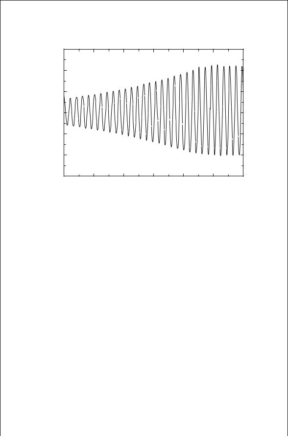
FIGURE 10.8 10 MHz Hartley oscillator time domain response. |
|||
*.TRAN |
step> <final |
time> <no print> |
||
>step ceiling> |
SKIPBP |
|
|
|
.TRAN |
2n 3uS |
0 |
7nS |
SKIPBP |
.PROBE |
|
|
|
|
.OP
.END
The result of the circuit analysis in Fig. 10.8 shows the oscillation building up to a steady state output after many oscillation periods.
10.5MINIMUM REQUIREMENTS OF THE REFLECTION COEFFICIENT
The two-port oscillator has two basic configurations: (1) a common source FET that uses an external resonator feedback from drain to gate and (2) a common gate FET that produces a negative resistance. In both of these the dc bias and the external circuit determine the oscillation conditions. When a load is connected to an oscillator circuit and the bias voltage is applied, noise in the circuit or start up transients excites the resonator at a variety of frequencies. However, only the resonant frequency is supported and sent back to the device negative resistance. This in turn is amplified and so the oscillation begins building up.
Negative resistance is merely a way of describing a power source. Ohm’s law says that the resistance of a circuit is the ratio of the voltage applied to the current