

12.General-purpose microprocessors
.pdfChapter 12 − General-Purpose Microprocessors Page 1 of 25
Table of Content
Table of Content ........................................................................................................................................................... |
1 |
||
12 |
General-Purpose Microprocessors .................................................................................................................... |
2 |
|
12.1 |
Overview of the CPU Design........................................................................................................................ |
2 |
|
12.2 |
Instruction Set ............................................................................................................................................... |
2 |
|
12.2.1 |
Two Operand Instructions..................................................................................................................... |
3 |
|
12.2.2 |
One Operand Instructions...................................................................................................................... |
3 |
|
12.2.3 Instructions Using a Memory Address.................................................................................................. |
3 |
||
12.2.4 |
Jump Instructions .................................................................................................................................. |
3 |
|
12.3 |
Datapath ........................................................................................................................................................ |
5 |
|
12.3.1 |
Input multiplexer................................................................................................................................... |
6 |
|
12.3.2 |
Conditional Flags .................................................................................................................................. |
6 |
|
12.3.3 |
Accumulator.......................................................................................................................................... |
6 |
|
12.3.4 |
Register File .......................................................................................................................................... |
6 |
|
12.3.5 |
ALU ...................................................................................................................................................... |
6 |
|
12.3.6 |
Shifter / Rotator..................................................................................................................................... |
7 |
|
12.3.7 |
Output Buffer ........................................................................................................................................ |
7 |
|
12.3.8 |
Control Word ........................................................................................................................................ |
7 |
|
12.3.9 VHDL Code for the Datapath ............................................................................................................... |
8 |
||
12.4 |
Control Unit .................................................................................................................................................. |
9 |
|
12.4.1 |
Reset.................................................................................................................................................... |
10 |
|
12.4.2 |
Fetch.................................................................................................................................................... |
10 |
|
12.4.3 |
Decode ................................................................................................................................................ |
10 |
|
12.4.4 |
Execute................................................................................................................................................ |
10 |
|
12.4.5 VHDL Code for the Control Unit........................................................................................................ |
11 |
||
12.5 |
CPU |
............................................................................................................................................................. |
20 |
12.6 |
Top-level Computer .................................................................................................................................... |
22 |
|
12.6.1 |
Input .................................................................................................................................................... |
22 |
|
12.6.2 |
Output ................................................................................................................................................. |
22 |
|
12.6.3 |
Memory............................................................................................................................................... |
22 |
|
12.6.4 |
Clock ................................................................................................................................................... |
23 |
|
12.6.5 VHDL Code for the Complete Computer ........................................................................................... |
23 |
||
12.7 |
Examples..................................................................................................................................................... |
24 |
|
Microprocessor Design – Principles and Practices with VHDL |
Last updated 3/18/2003 8:01 PM |

Chapter 12 − General-Purpose Microprocessors |
Page 2 of 25 |
12 General-Purpose Microprocessors
Unlike a dedicated or custom microprocessor that is capable of performing only one function, a general-purpose microprocessor is capable of performing many different functions under the direction of instructions. Given a different instruction set or program, the general-purpose microprocessor will perform a different function. On the other hand, a general-purpose microprocessor can also be viewed as a dedicated microprocessor because it is made to perform only one function, and that is to execute the software instructions. In this sense, we can design and construct our general-purpose microprocessor in the same way that we constructed our dedicated microprocessors as discuss in the previous chapter.
Control |
Data |
|
Inputs |
Inputs |
|
Control unit |
|
'0' Datapath |
|
1 |
0 |
ff |
s |
y |
|
|
|
Next- |
State |
Output |
|
ALU |
|
Memory |
Logic |
Control |
|||
state |
|
||||
Logic |
register |
|
Signals |
ff |
|
|
|
|
|
register |
Status
Signals
Control |
Data |
Outputs |
Outputs |
12.1 Overview of the CPU Design
A general-purpose microprocessor is often referred to as the central processing unit (CPU). The CPU is simply a dedicated microprocessor that only executes software instructions. In designing a CPU, we must first define its instruction set and how the instructions are encoded and executed. We need to answer questions such as how many instructions do we want? What are the instructions? What operation code (opcode) do we assign to each of the instructions? How many bits do we use to encode an instruction?
Once we have decided on the instruction set, we can proceed to designing a datapath that can execute all the instructions in the instruction set. In this step we are creating a custom datapath, so we need to answer questions such as what functional units do we need? How many registers do we need? Do we use a single register file or separate registers? How the different units are connected together?
Finally, we can design the control unit. Just like the dedicated microprocessor, the control unit asserts the control signals to the datapath. This finite-state machine cycles through three main steps or states: 1) fetch an instruction; 2) decode the instruction; and 3) execute the instruction. The control unit performs these steps by sending the appropriate control signals to the datapath or to external devices.
Instructions in your program are usually stored in external memory, so in addition to the CPU, there is external memory that is connected to the CPU via an address bus and a data bus. Hence, step 1 (fetch an instruction) usually involves the control unit setting up a memory address on the address bus and telling the external memory to output the instruction from that memory location onto the data bus. The control unit then reads the instruction from the data bus. To keep our design simple, instead of having external memory, we will put the memory directly inside the CPU and implemented simply as a 64-byte array. In fact, there are real CPUs with internal program memory.
For step 2 (decode the instruction) the control unit extracts the opcode bits from the instruction and determines what the current instruction is by jumping to the state that has been assigned for executing that instruction. Once in that particular state, the finite-state machine performs step 3 by simply asserting the appropriate control signals for controlling the datapath to execute that instruction.
12.2 Instruction Set
The instructions that our general-purpose microprocessor can execute and the corresponding encoding are defined in Figure 1. The Instruction column shows the syntax and mnemonic to use for the instruction when writing a program in assembly language. The Encoding column shows the binary encoding for the instructions and the Operation column shows the actual operation of the instruction. The instructions are separated into four categories:
1)data movement instructions for transferring data between the accumulator, the general registers and the memory;
2)jump instructions for changing the instruction execution sequence; 3) arithmetic and logical instructions for performing arithmetic and logics; and 4) input / output and miscellaneous instructions. There are five data movement instructions, eight jump instructions, ten arithmetic and logic instructions, two input/output instructions, and two miscellaneous instructions.
Microprocessor Design – Principles and Practices with VHDL |
Last updated 3/18/2003 8:01 PM |
Chapter 12 − General-Purpose Microprocessors |
Page 3 of 25 |
The number of instructions implemented determines the number of bits required to encode all the instructions. All instructions are encoded using one byte except for instructions that have a memory address as one of its operand, in which case a second byte for the address is needed. The encoding scheme uses the first four bits as the opcode. Depending on the opcode, the last four bits are interpreted differently as follows.
12.2.1 Two Operand Instructions
If the instruction requires two operands, it always uses the accumulator (A) for one operand. If the second operand is a register then the last three bits in the encoding specifies the register file number. An example of this is the LDA (load accumulator from register) instruction where it loads the accumulator with the content of the register file number specified in the last three bits of the encoding. Another example is the ADD (add) instruction where it adds the content of the accumulator with the content of the specified register file and put the result in the accumulator. The result of all arithmetic and logical operations is stored in the accumulator.
The LDI (load accumulator with immediate value) is also a two-operand instruction. However, the second operand is an immediate value that is obtained from the second byte of the instruction itself (iiiiiiii). These eight bits are interpreted as a signed number and is loaded into the accumulator.
12.2.2 One Operand Instructions
One-operand instructions always use the accumulator and the result is stored back in the accumulator. In this case, the last four bits in the encoding are used to further decode the instruction. An example of this is the INC (increment accumulator) instruction. The opcode (1110) is used by all the one-operand arithmetic and logical instructions. The last four bits (0001) specify the INC instruction.
12.2.3 Instructions Using a Memory Address
For instructions that have a memory address as one of its operand, an additional six bits are needed in order to access the 64 bytes of memory space. These six bits (aaaaaa) are specified in the six least significant bits of the second byte of the instruction. An example is the LDM (load accumulator from memory) instruction. The address of the memory location where the data is to be loaded from is specified in the second byte. In this case, the last four bits of the first byte and the first two bits in the second byte are not used and are always set to 0. All the absolute jump instructions follow this format.
12.2.4 Jump Instructions
For jump instructions, the last four bits of the encoding also serves to differentiate between absolute and relative jumps. If the last four bits are zeros, then it is an absolute jump, otherwise, they represent a sign and magnitude format relative displacement from the current location as specified in the program counter (PC). For example, the two-byte encoding 0110 0000 0000 0100 specifies an absolute unconditional jump to memory location 4. The first four bits (0110) specify the unconditional jump. The second four bits (0000) specify an absolute jump. The last six bits (000100) specify the memory address 4. On the other hand, the one-byte encoding 0110 0100 specifies a relative unconditional jump to PC + 4. Again, the first four bits (0110) specify the unconditional jump. The next four bits (0100) specify that it is a relative jump because it is not zero. The relative position to jump to is +4 because the first bit is a 0, which is for forward and the last three bits evaluate to 4. To jump backward by four locations, we would use 1100 instead.
Two conditional flags (zero and positive) are used for conditional jumps. These flags are set or reset depending on the value of the accumulator when the accumulator is written to. Instructions that modify the accumulator include LDA, LDM, LDI, all the arithmetic and logic instructions, and IN. For example, if the result of the ADD instruction is a positive number, then the zero flag will be reset and the positive flag will be set. A conditional jump then reads the value of these flags to see whether to jump or not. The JZ instruction will not jump after the previous ADD instruction, where as the JP instruction will perform the jump.
Microprocessor Design – Principles and Practices with VHDL |
Last updated 3/18/2003 8:01 PM |

Chapter 12 − General-Purpose Microprocessors |
Page 4 of 25 |
|
||||||
|
|
|
|
|
|
|
||
Instruction |
|
Encoding |
Operation |
Comment |
|
|||
Data movement instructions |
|
|
|
|
|
|||
LDA A,rrr |
|
0001 0rrr |
A ← |
R[rrr] |
Load accumulator from register |
|
||
STA rrr,A |
|
0010 0rrr |
R[rrr] ← |
A |
Load register from accumulator |
|
||
LDM A,aaaaaa |
|
0011 0000 |
|
A ← |
M[aaaaaa] |
Load accumulator from memory |
|
|
|
|
00aaaaaa |
|
|
|
|
|
|
STM aaaaaa,A |
|
0100 0000 |
|
M[aaaaaa] ← A |
Load memory from accumulator |
|
||
|
|
00 aaaaaa |
|
|
|
|
|
|
LDI A,iiiiiiii |
|
0101 0000 |
|
A ← |
iiiiiiii |
Load accumulator with immediate |
|
|
|
|
iiiiiiii |
|
|
|
value (iiiiiiii is a signed number) |
|
|
Jump instructions |
|
|
|
|
|
|
|
|
JMP absolute |
|
0110 0000 |
|
PC = aaaaaa |
Absolute unconditional jump |
|
||
|
|
00 aaaaaa |
|
|
|
|
|
|
JMPR relative |
|
0110 smmm |
|
if (smmm != 0) then |
Relative unconditional jump (smmm |
|
||
|
|
|
|
if (s == 0) then PC = PC + mmm |
is in sign and magnitude format) |
|
||
|
|
|
|
else PC = PC – mmm |
|
|
||
JZ absolute |
|
0111 0000 |
|
if (A == 0) then PC = aaaaaa |
Absolute jump if A is zero |
|
||
|
|
00 aaaaaa |
|
|
|
|
|
|
JZR relative |
|
0111 smmm |
|
if (A == 0 and smmm != 0) then |
Relative jump if A is zero (smmm is |
|
||
|
|
|
|
if (s == 0) then PC = PC + mmm |
in sign and magnitude format) |
|
||
|
|
|
|
else PC = PC – mmm |
|
|
||
JNZ absolute |
|
1000 0000 |
|
if (A != 0) then PC = aaaaaa |
Absolute jump if A is not zero |
|
||
|
|
00 aaaaaa |
|
|
|
|
|
|
JNZR relative |
|
1000 smmm |
|
if (A != 0 and smmm != 0) then |
Relative jump if A is not zero |
|
||
|
|
|
|
if (s == 0) then PC = PC + mmm |
(smmm is in sign and magnitude |
|
||
|
|
|
|
else PC = PC – mmm |
format) |
|
||
JP absolute |
|
1001 0000 |
|
if(A == positive) then PC = aaaaaa |
Absolute jump if A is positive |
|
||
|
|
00 aaaaaa |
|
|
|
|
|
|
JPR relative |
|
1001 smmm |
|
if(A == positive and smmm != 0) then |
Relative jump if A is positive (smmm |
|
||
|
|
|
|
if (s == 0) then PC = PC + mmm |
is in sign and magnitude format) |
|
||
|
|
|
|
else PC = PC – mmm |
|
|
||
Arithmetic and logical instructions |
|
|
|
|
||||
AND A,rrr |
|
1010 0rrr |
A ← A AND R[rrr] |
Accumulator AND register |
|
|||
OR A,rrr |
|
1011 0rrr |
A ← A OR R[rrr] |
Accumulator OR register |
|
|||
ADD A,rrr |
|
1100 0rrr |
A ← |
A + R[rrr] |
Accumulator + register |
|
||
SUB A,rrr |
|
1101 0rrr |
A ← |
A − |
R[rrr] |
Accumulator − register |
|
|
NOT A |
|
1110 0000 |
|
A ← |
NOT A |
Invert accumulator |
|
|
INC A |
|
1110 0001 |
|
A ← A + 1 |
Increment accumulator |
|
||
DEC A |
|
1110 0010 |
|
A ← |
A − |
1 |
Decrement accumulator |
|
SHFL A |
|
1110 0011 |
|
A ← A << 1 |
Shift accumulator left |
|
||
SHFR A |
|
1110 0100 |
|
A ← A >> 1 |
Shift accumulator right |
|
||
ROTR A |
|
1110 0101 |
|
A ← |
Rotate_right(A) |
Rotate accumulator right |
|
|
Input / Output and Miscellaneous |
|
|
|
|
|
|||
In A |
|
1111 0000 |
|
A ← |
input |
Input to accumulator |
|
|
Out A |
|
1111 0001 |
|
output ← |
A |
Output from accumulator |
|
|
HALT |
|
1111 0010 |
|
Halt |
|
|
Halt execution |
|
NOP |
|
0000 0000 |
|
no operation |
No operation |
|
||
Microprocessor Design – Principles and Practices with VHDL |
Last updated 3/18/2003 8:01 PM |
Chapter 12 − General-Purpose Microprocessors |
Page 5 of 25 |
Notations:
A = accumulator.
R = general register. M = memory.
PC = program counter.
rrr = three bits for specifying the general register number (0 – 7). aaaaaa = six bits for specifying the memory address.
iiiiiiii = an eight bit signed number.
smmm = four bits for specifying the relative jump displacement in sign and magnitude format. The most significant bit (s) determines whether to jump forward or backward (0 = forward, 1 = backward). The last three bits (mmm) specify the number of locations to increment or decrement from the current PC location.
Figure 1. Instruction set for the general-purpose microprocessor.
12.3 Datapath
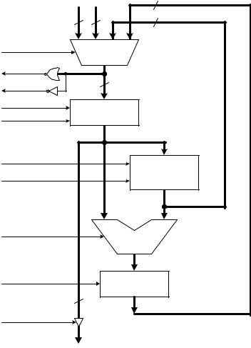
Having defined the instruction set for our general microprocessor, we are now ready to design the custom datapath that can execute all the operations as defined by all the instructions. We will follow the method described in Chapter 8 for designing a custom datapath at the register-transfer level. The resulting datapath is shown in Figure 2.
|
imm_dp |
input_dp |
|
|
|
|||
|
|
|
|
|
|
|
8 |
|
|
8 |
|
8 |
|
|
|
8 |
|
|
|
|
|
|
|
|
|
|
muxsel_dp1,0 |
3 |
|
|
2 |
1 |
|
0 |
|
|
sel1,0 |
Mux |
|
|
|
|||
zero_dp |
|
|
|
|
y |
|
|
|
|
|
|
|
C_muxout |
|
|||
|
|
|
|
|
|
|||
positive_dp |
MSB |
|
|
8 |
|
|
|
|
accwr_dp |
wr |
Accumulator |
|
|
||||
rst_dp |
|
|
||||||
clear |
|
|
|
|
|
|
||
|
|
|
|
|
|
|
||
|
|
|
|
|
C_accout |
|
||
rfwr_dp |
|
|
|
|
|
|
wr |
8 |
|
|
|
|
|
|
|
||
rfaddr_dp2,1,0 |
|
|
|
|
|
|
Register File |
|
|
|
|
|
|
|
|
addr2,1,0 |
|
|
|
|
|
|
|
|
|
C_rfout |
alusel_dp2,1,0 |
|
|
|
|
A |
|
B |
|
|
|
|
|
sel2,1,0 |
ALU |
|
||
|
|
|
|
|
|
|||
|
|
|
|
|
|
|
C_aluout |
|
shiftsel_dp1,0 |
|
|
|
|
sel1,0 |
Shifter |
|
|
|
|
|
|
|
|
|||
|
8 |
|
|
|
|
|
C_shiftout |
|
outen_dp |
|
|
|
|
|
|
|
|
output_dp
Figure 2. Datapath.
Microprocessor Design – Principles and Practices with VHDL |
Last updated 3/18/2003 8:01 PM |
Chapter 12 − General-Purpose Microprocessors |
Page 6 of 25 |
The width of the datapath is eight bits, i.e. all the connections for data movement are eight bits wide. In the figure, they are the thicker lines. The remaining thinner control lines are all one bit wide unless the name for that
control line has a number subscript such as rfaddr_dp2,1,0, in which case there are as many lines as the subscript numbers. For example, the control line label rfaddr_dp2,1,0 is actually composed of three separate lines.
12.3.1 Input multiplexer
The 4-to-1 input mux at the top of the datapath drawing selects one of four different inputs to be written into the accumulator. These four inputs, starting from the left, are: (1) imm_dp for getting the immediate value from the LDI instruction and storing it into the accumulator; (2) input_dp for getting a user input value for the IN instruction; (3) the next input selection allows the content of the register file to be written to the accumulator as used by the LDA instruction; (4) allows the result of the ALU and the shifter to be written to the accumulator as used by all the arithmetic and logical instructions.
12.3.2 Conditional Flags
The two conditional flags, zero and positive, are set by two comparators that check the value at the output of the mux which is the value that is to be written into the accumulator for these two conditions. To check for a value being zero, recall that just a NOR gate will do. In our case, we need an eight-input NOR gate because of the 8-bit wide databus. To check for a positive number, we simply need to look at the most significant sign bit. A 2’s complement positive number will have a zero sign bit, so a single inverter connected to the most significant bit of the databus is all that is needed to generate this positive flag signal.
12.3.3 Accumulator
The accumulator is a standard 8-bit wide register with a write wr and clear clear control input signals. The write signal, connected to accwr_dp, is asserted whenever we want to write a value into the accumulator. The clear signal is connected to the main computer reset signal rst_dp, so that the accumulator is always cleared on reset. The content of the accumulator is always available at the accumulator output. The value from the accumulator is sent to three different places: (1) it is sent to the output buffer for the OUT instruction; (2) it is used as the first (A) operand for the ALU; and (3) it is sent to the input of the register file for the STA instruction.
12.3.4 Register File
The register file has eight locations, each 8-bits wide. Three address lines, rfaddr_dp2, rfaddr_dp1, rfaddr_dp0, are used to address the eight locations for both reading and writing. There are one read port and one write port. The read port is always active which means that it always has the value from the currently selected address location. However, to write to the selected location, the write control line rfwr_dp must be asserted before a value is written to the currently selected address location.
Note that a separate read and write address lines is not required because all the instructions either perform just a read from the register file or a write to the register file. There is no one instruction that performs both a read and a write to the register file. Hence, only one set of address lines is needed for determining both the read and write locations.
12.3.5 ALU
The ALU has eight operations implemented as defined by the following table. The operations are selected by the three select lines alusel_dp2, alusel_dp1, and alusel_dp0.
alusel_dp2 |
alusel_dp 1 |
alusel_dp 0 |
Operation Name |
Operation |
Instruction |
0 |
0 |
0 |
Pass |
Pass A to output |
non-ALU instructions |
0 |
0 |
1 |
AND |
A AND B |
AND A,rrr |
0 |
1 |
0 |
OR |
A OR B |
OR A,rrr |
0 |
1 |
1 |
NOT |
A' |
NOT A |
1 |
0 |
0 |
Addition |
A + B |
ADD A,rrr |
Microprocessor Design – Principles and Practices with VHDL |
Last updated 3/18/2003 8:01 PM |
Chapter 12 − General-Purpose Microprocessors |
|
|
Page 7 of 25 |
|||||
|
|
|
|
|
|
|
|
|
1 |
0 |
1 |
|
Subtraction |
A – B |
SUB A,rrr |
||
|
1 |
1 |
0 |
|
Increment |
A + 1 |
INC A |
|
|
1 |
1 |
1 |
|
Decrement |
A – 1 |
DEC A |
|
The select lines are asserted by the corresponding ALU instructions as shown under the Instruction column in the above table. The pass through operation is used by all non-ALU instructions.
12.3.6 Shifter / Rotator
The Shifter has four operations implemented as defined by the following table. The operations are selected by the two select lines shiftsel_dp1, and shiftsel_dp0.
shiftsel_dp1 |
shiftsel_dp0 |
Operation |
Instruction |
0 |
0 |
Pass through |
non Shift/Rot instructions |
0 |
1 |
Shift left and fill with 0 |
SHFL A |
1 |
0 |
Shift right and fill with 0 |
SHFR A |
1 |
1 |
Rotate right |
ROTR A |
The select lines are asserted by the corresponding Shifter/Rotator instructions as shown under the Instruction column in the above table. The pass through operation is used by all non-Shifter/Rotator instructions.
12.3.7 Output Buffer
The output buffer is a register with an enable control signal connected to outen_dp. Whenever the enable line is asserted, the output from the accumulator is stored into the buffer. The value stored in the output buffer is used as the output for the computer and is always available. The enable line is asserted either by the OUT A instruction or by the system reset signal.
12.3.8 Control Word
From Figure 2, we see that the control word for this custom datapath has fourteen bits, which maps to the control signals for the different datapath components. These fourteen control signals are summarized in Figure 3.
Number |
Signal Name |
Component |
Purpose |
14 |
muxsel_dp1 |
4-input mux |
Select line 1 |
13 |
muxsel_dp 0 |
4-input mux |
Select line 0 |
12 |
accwr_dp |
accumulator |
Write enable |
11 |
rst_dp |
accumulator |
Clear |
10 |
rfwr_dp |
register file |
Write enable |
9 |
rfaddr_dp 2 |
register file |
Address line 2 |
8 |
rfaddr_dp 1 |
register file |
Address line 1 |
7 |
rfaddr_dp 0 |
register file |
Address line 0 |
6 |
alusel_dp 2 |
ALU |
Select line 2 |
5 |
alusel_dp 1 |
ALU |
Select line 1 |
4 |
alusel_dp 0 |
ALU |
Select line 0 |
3 |
shiftsel_dp 1 |
Shifter |
Select line 1 |
2 |
shiftsel_dp 0 |
Shifter |
Select line 0 |
1 |
outen_dp |
Tri-state buffer |
Output enable |
Figure 3. Control word signals for the datapath
By now, you should be able to trace through this datapath and see how it executes for each of the instructions. For example, to execute the ADD instruction, which adds the content of the accumulator with the content of the specified register file location and writes the result back into the accumulator, the value in the accumulator is passed to the A operand of the ALU. The B operand of the ALU comes from the register file, the location of which is
Microprocessor Design – Principles and Practices with VHDL |
Last updated 3/18/2003 8:01 PM |

Chapter 12 − General-Purpose Microprocessors |
Page 8 of 25 |
selected from setting the register file address lines rfaddr_dp2,1,0. The appropriate ALU select lines alusel_dp2,1,0 are set to select the ADD operation. The shifter is not needed and so the pass through operation is selected. The output
of the shifter is routed back through input 0 of the multiplexer and finally written back to the accumulator.
So the control word for the instruction
ADD A,011
is
muxsel1 |
muxsel0 |
accwr |
rst |
rfwr |
rfaddr2 |
rfaddr1 |
rfaddr0 |
alusel2 |
alusel1 |
alusel0 |
shiftsel1 |
shiftsel0 |
outen |
0 |
0 |
1 |
0 |
0 |
0 |
1 |
1 |
1 |
0 |
0 |
0 |
0 |
0 |
12.3.9 VHDL Code for the Datapath
Structural VHDL coding is used to connect all the components together to form the custom datapath for our general microprocessor. The VHDL code is shown in Listing 1.
LIBRARY ieee;
USE ieee.std_logic_1164.all;
ENTITY dp IS PORT ( clk_dp: IN std_logic; rst_dp: IN std_logic;
muxsel_dp: IN std_logic_vector(1 DOWNTO 0); imm_dp: IN std_logic_vector(7 DOWNTO 0); input_dp: IN std_logic_vector(7 DOWNTO 0); accwr_dp: IN std_logic;
rfaddr_dp: IN std_logic_vector(2 DOWNTO 0); rfwr_dp: IN std_logic;
alusel_dp: IN std_logic_vector(2 DOWNTO 0); shiftsel_dp: IN std_logic_vector(1 DOWNTO 0); outen_dp: IN std_logic;
zero_dp: OUT std_logic; positive_dp: OUT std_logic;
output_dp: OUT std_logic_vector(7 DOWNTO 0)); END dp;
ARCHITECTURE struct OF dp is
COMPONENT mux4 PORT (
sel_mux: IN std_logic_vector(1 DOWNTO 0); in3_mux,in2_mux,in1_mux,in0_mux: IN std_logic_vector(7 DOWNTO 0); out_mux: OUT std_logic_vector(7 DOWNTO 0));
END COMPONENT;
COMPONENT acc PORT ( clk_acc: IN std_logic; rst_acc: IN std_logic; wr_acc: IN std_logic;
input_acc: IN std_logic_vector (7 DOWNTO 0); output_acc: OUT std_logic_vector (7 DOWNTO 0));
END COMPONENT;
COMPONENT reg_file PORT ( clk_rf: IN std_logic; wr_rf: IN std_logic;
addr_rf: IN std_logic_vector(2 DOWNTO 0); input_rf: IN std_logic_vector(7 DOWNTO 0);
Microprocessor Design – Principles and Practices with VHDL |
Last updated 3/18/2003 8:01 PM |

Chapter 12 − General-Purpose Microprocessors |
Page 9 of 25 |
output_rf: OUT std_logic_vector(7 DOWNTO 0)); END COMPONENT;
COMPONENT alu PORT (
sel_alu: IN std_logic_vector(2 DOWNTO 0); inA_alu: IN std_logic_vector(7 DOWNTO 0); inB_alu: IN std_logic_vector(7 DOWNTO 0); OUT_alu: OUT std_logic_vector (7 DOWNTO 0));
END COMPONENT;
COMPONENT shifter PORT (
sel_shift: IN std_logic_vector(1 DOWNTO 0); input_shift: IN std_logic_vector(7 DOWNTO 0); output_shift: OUT std_logic_vector(7 DOWNTO 0));
END COMPONENT;
COMPONENT tristatebuffer PORT (
E: IN std_logic;
D: IN std_logic_vector(7 DOWNTO 0);
Y: OUT std_logic_vector(7 DOWNTO 0));
END COMPONENT;
SIGNAL C_aluout,C_accout,C_rfout,C_muxout,C_shiftout: std_logic_vector(7 DOWNTO 0);
SIGNAL C_outen: std_logic;
BEGIN
U0: mux4 PORT MAP(muxsel_dp,imm_dp,input_dp,C_rfout,C_shiftout,C_muxout); U1: acc PORT MAP(clk_dp,rst_dp,accwr_dp,C_muxout,C_accout);
U2: reg_file PORT MAP(clk_dp,rfwr_dp,rfaddr_dp,C_accout,C_rfout);
U3: alu PORT MAP(alusel_dp,C_accout,C_rfout,C_aluout); U4: shifter PORT MAP(shiftsel_dp,C_aluout,C_shiftout); C_outen <= outen_dp OR rst_dp;
U5: tristatebuffer PORT MAP(C_outen,C_accout,output_dp); --output_dp <= C_accout;
zero_dp <= '1' WHEN (C_muxout = "00000000") ELSE '0'; positive_dp <= NOT C_muxout(7);
--positive_dp <= '1' WHEN (C_muxout(7) = '0') ELSE '0'; END struct;
Listing 1. Datapath.
12.4 Control Unit
The finite state machine for the control unit basically cycles through four main states: reset, fetch, decode, and execute, as shown in Figure 4. There is one execute state for each instruction in the instruction set.
Microprocessor Design – Principles and Practices with VHDL |
Last updated 3/18/2003 8:01 PM |

Chapter 12 − General-Purpose Microprocessors |
Page 10 of 25 |
|
|
reset |
|
|
fetch |
|
|
decode |
|
execute |
execute |
execute |
LDA |
ADD |
JMP |
Figure 4. State diagram for the control unit.
12.4.1 Reset
The finite state machine starts executing from the reset state when the reset signal is asserted. On reset, the finite state machine initializes all its working variables and control signals. The variables include:
•PC – program counter
•IR – instruction register
•state – the state variable
In addition, the content of the memory, i.e., the program for the computer to execute is also loaded at this time.
12.4.2 Fetch
In the fetch state, the memory content of the location pointed to by the PC is loaded into the instruction register. The PC is then incremented by one to prepare it for fetching the next instruction. If the fetched instruction is a jump instruction, then the PC will be changed accordingly during the execution phase.
12.4.3 Decode
The content that is stored in the instruction register is decoded according to the encoding that is assigned to the instructions as listed in Figure 1. This is accomplished in VHDL using a CASE statement with the switch condition being the opcode. From the different cases, the state that is responsible for executing the corresponding instruction is assigned to the next state variable. As a result, the instruction will be executed starting at the beginning of the next clock cycle when the FSM enters this new state.
12.4.4 Execute
The execution state simply sets up the control word, which asserts the appropriate control signals for the datapath to carry out the necessary operations for executing a particular instruction. Each instruction, therefore, has its own execute state. For example, the execute state for the add instruction ADD A,011 will set up the following control word.
muxsel1 |
muxsel0 |
accwr |
rst |
rfwr |
rfaddr2 |
rfaddr1 |
rfaddr0 |
alusel2 |
alusel1 |
alusel0 |
shiftsel1 |
shiftsel0 |
outen |
0 |
0 |
1 |
0 |
0 |
0 |
1 |
1 |
1 |
0 |
0 |
0 |
0 |
0 |
For all the jump instructions, no actions need to be taken by the datapath. It simply determines whether to perform the jump or not depending on the particular jump instruction and by checking on the zero and positive flags. If a jump is needed then the target address is calculated and then assigned to the PC.
Microprocessor Design – Principles and Practices with VHDL |
Last updated 3/18/2003 8:01 PM |