

12.Phase Lock Loops
.pdfRadio Frequency Circuit Design. W. Alan Davis, Krishna Agarwal
Copyright 2001 John Wiley & Sons, Inc.
Print ISBN 0-471-35052-4 Electronic ISBN 0-471-20068-9
CHAPTER TWELVE
Phase Lock Loops
12.1INTRODUCTION
Phase lock loops (PLL) are not a recent invention. Their use became widespread with the availability of high-quality integrated circuit operational amplifiers (opamps) in the 1960s. This versatile circuit has found applications across the frequency spectrum in consumer, commercial, deep space, and military projects. Tracking Voyager through the solar system and tuning a car radio are made to order uses for a PLL. To understand a PLL, a good working knowledge of RF techniques, oscillator design, closed loop control theory, analog circuit design, and digital circuit design is required. A comprehension of each of the components and its place in the system is essential. Fortunately not all of this knowledge is required at once. The books listed at the end of this chapter can each provide an in-depth insight into areas beyond the present scope [1–5]. This discussion will begin with the basic concepts and rapidly expand these ideas into practical considerations.
12.2PLL DESIGN BACKGROUND
Discussion of the PLL draws heavily on many other areas of analysis, which includes an understanding of the principles of closed loop control theory. From control theory comes the concept of negative feedback to tailor the performance of closed loop systems. Response time, transient performances, bandwidth, damping ratio, and phase margin are used to describe PLL operation. The type and order of a closed loop system define the complexity and response to a stimulus.
In most PLL’s, at least two of the components, the voltage-controlled oscillator (VCO) and phase detector, are high-frequency components. There may also be amplifiers, mixers, frequency multipliers, and other oscillators. To use these items, a familiarity with RF design practices and terminology is important.
Frequency multiplication may require digital integrated circuits (ICs) within the PLL. These ICs require digital control words to set the desired frequency.
247

248 PHASE LOCK LOOPS
Many integrated circuits are presently available that combine many of the PLL functions on a single chip. Most of the interface control is digital.
Analog circuit design is perhaps the most demanding of the circuit areas within a PLL. Op-amps are used in many of the filtering circuits used within a loop. Inverting and noninverting circuits are required for loop filters and search circuits. Integrators, dc amplifiers, Schmitt triggers, and offset circuits are used to set the loop operation. Resistor/capacitor circuits provide phase shift for stability. The oscillator is an intrinsic part of a PLL, and its design in itself is a specialized and technically challenging area.
12.3PLL APPLICATIONS
A phase lock loop is a frequency domain device that can be used to multiply, divide, or filter different frequencies. Consider a space probe rapidly moving away from the earth. To recover data from the probe, the transmitter frequency must be known. The signal is very weak because of the distance, and the low signal-to-noise ratio requires a very small receiver filter bandwidth to recover the data. However, because of the relative motion, there is a significant and changing Doppler shift to the transmit frequency. The system requires a filter that may be only a few Hertz wide operating at a varying frequency that is centered at several GHz.
An electronic phase lock loop is one form of a closed loop system. The cruise control is another. A switching power supply, a camera’s light meter, a radio’s automatic gain control, the temperature control in a building, a car’s emission system controls, and a Touch-Tone dialing system are examples of closed loop systems. A broadcast receiver changes frequency with a button push or electronically. Each time the station is accurately centered with no manual adjustment required. Physically these PLLs are all very different working at different jobs and in different environments. However, they all must follow the same rules, and the loops must all be stable.
A clear understanding of the concept of feedback control is illustrated by an everyday situation of the simple action of controlling the speed of a car. If the desired speed is 60 mph, then this becomes the reference. Any deviation from this speed is an error. The accelerator pedal is the control element. On level terrain, a constant pressure on the pedal will maintain constant speed. As the car goes up a hill, it will slow down. The difference between the actual speed and the reference value generates an error. This error generates a command to push the accelerator pedal. Pushing the pedal will increase the speed, but there will continue to be a slight error. As the car crests the hill and starts down, the speed will increase. Releasing pedal pressure will slow the acceleration, but an error will remain until a steady state condition is again reached. For this example, the driver’s brain is the feedback path. The driver controls the sense of the feedback by knowing when to push and when to release the pedal. By his reaction time, he controls how close to the reference he maintains the car’s speed. He may

PLL BASICS |
249 |
decide to rapidly change the correction to tightly match the desired speed, or he may choose to compensate slowly so his speed averages out to the correct value. His actions coupled with the car’s controls form a system closely analogous to a phase lock loop. Replace the human with an electrical circuit that senses the speed error, include another circuit that tempers the response time, and couple it to the accelerator controls. This is the typical cruise control system. The elements of understanding the operation of a phase lock loop are all available here. The next step is to apply the concepts of this example to the classical elements that make up a PLL.
12.4PLL BASICS
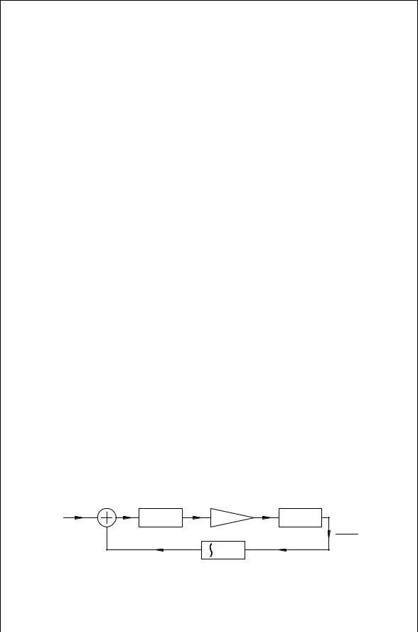
A PLL is a closed loop system used for frequency control. Several building blocks are common to most PLL designs:
1.The phase detector
2.The loop filter
3.The voltage-controlled oscillator
Figure 12.1 illustrates the connection of these blocks to make a complete phase lock loop. The phase detector has two inputs and one output. This block can be realized by a specialized mixer described in Chapter 11 where the IF port passband goes down to dc. If the two input signals are very close in frequency, then the output will contain a term at twice the input frequency and a term that is almost zero frequency. The loop error signal in the PLL is the near-zero term. This signal contains everything that is needed to control the VCO. This error signal goes to the loop filter for amplification and frequency limiting. The loop filter may be as simple as a capacitor and a resistor, or it can be one or more operational amplifiers with many resistors and capacitors. The loop filter is generally a simple circuit that requires an in depth analysis. It is the “glue” that holds all the other parts together and makes the PLL work the way it is supposed to work. The VCO is the control element of this loop. The input is a control voltage from the loop filter, while the output is the required frequency.
Phase
Detector
fref |
Loop |
VCO |
fout |
|
Filter |
||||
|
|
|
FIGURE 12.1 Basic phase lock loop.

250 PHASE LOCK LOOPS
Frequency is the time rate of change of phase, so phase is the time integral of frequency. Consequently, if the frequency of the VCO is proportional to the tuning voltage, the output phase is proportional to the integral of tuning voltage. The output frequency can range from a few Hertz to many GHz. The VCO output becomes the second input to the phase detector.
When the loop is first turned on, the VCO frequency is not controlled. The loop filter output voltage can be anywhere between the high and low limits set by the power supply. However, the phase detector produces an error voltage that is the difference between the VCO frequency and the reference frequency. Like the cruise control example, this signal tells the loop filter whether the VCO is going too fast or too slow relative to the reference frequency. The loop filter is “smart enough” to know what to do. If the error signal indicates that the VCO frequency is less than the reference, the loop filter adjusts the control voltage to raise the VCO frequency. If the VCO frequency is too high, the loop filter changes the voltage and lowers the VCO frequency. The loop filter design sets how fast this happens. Some loops may be designed for a fast bumpy ride, while others may require a slow smooth ride. When the loop filter has done its job, the VCO frequency will exactly match the reference frequency, and the two inputs will have a constant phase difference. This match in frequency and constant phase difference will be maintained even if the reference frequency changes. With each change, the PLL again goes through the settling out process. If the reference is noisy, the PLL is in a continual state of change, working hard to follow the input. If a PLL were nothing more than a box with the same frequency in and out, it would not be much of an invention. Happily there is a lot more to it than that. Before preceding any farther, the basic idea of the frequency control by a closed loop operation must be clarified.
12.5LOOP DESIGN PRINCIPLES
There are many design rules that go into a successful, stable closed loop design, but many of these details are beyond the scope of his text. However, this discussion will lead to an understanding of how the loop works and how to select parts to customize its operation. From the overall system point of view, the PLL designer must know the overall requirements and be able to translate these requirements into the PLL parameters for the design.
With a PLL, the important top-level parameters are the input and output frequency, the response time, the loop bandwidth and the loop damping ratio. The top-level view concentrates on these system level values. The detailed aspects of the phase detector and VCO must be considered. These are usually highfrequency parts requiring high-frequency design techniques. The design of the loop filter requires an understanding of analog design techniques. Figure 12.2 illustrates the PLL block diagram, which includes a frequency divider in the feedback path. Both frequencies coming into the phase detector must be the locked together at the same frequency. This will force the output frequency,

|
|
|
PLL COMPONENTS |
251 |
|
Phase |
|
|
|
|
Detector |
|
|
|
fref |
Loop |
VCO |
fout |
|
Filter |
|
|||
|
|
|
|
Divide
by N
FIGURE 12.2 Phase lock loop with a frequency divider.
fout, to be N times the reference frequency, fref. Familiarity with digital circuit design is required to complete the design. A PLL design is not just a system design nor an RF design nor an analog design, but it is a combination of all these areas. The actual design process can be summarized by three principles.
1.Know each component. The components of a PLL, the VCO, phase detector, loop filter, and frequency divider must be thoroughly understood and tested as stand-alone individual components. Testing of the actual parts must show that they each meet the design goals. These tests may extend far beyond the information on the manufacturer’s data sheet.
2.Test the components together. The individual components must work correctly when connected together in an open loop configuration. The loop filter must put out enough voltage to drive the VCO. The VCO must have enough output to drive the frequency divider. The phase detector output must be large enough for the loop filter to use. An open loop analysis must show the correct phase margin and bandwidth for stability. These issues are resolved with an open loop analysis.
3.Compare the closed loop configuration to the design goals. A closed loop analysis should show that the final connection matches the system level design goals. Both test measurement techniques and analysis can be applied for PLL design verification.
12.6PLL COMPONENTS
The basic building blocks, except in exotic applications, are those shown in Fig. 12.2. This section describes in greater depth each of these functions.
12.6.1Phase Detectors
Phase detectors come in many configurations. These include those with logic level inputs, passive and active analog versions, and sampling versions used for highfrequency multiplication. In addition there are phase detectors with automatic

252 PHASE LOCK LOOPS
frequency search features to aid in initial frequency acquisition. In its simplest form, a phase detector is a frequency mixer. As described in Chapter 11, when two signals come into the mixer, the output consists primarily in the sum and difference frequencies. The sum frequency is filtered out by the loop filter. The difference frequency, historically called the beat note, is typically a few kHz or less in a PLL. If the two input frequencies are exactly the same, the phase detector output is the phase difference between the two inputs. This loop error signal is filtered and used to control the VCO frequency. The two input signals can be represented by sine waves:
V1 |
D Va sin ω1t C 1 |
12.1 |
V2 |
D Vb sin ω2t C 2 |
12.2 |
The difference frequency term is the error voltage given as
Ve D Km Ð V1 Ð V2 D |
KmVaVb |
cos[ ω1 ω2 t C 1 2 ] |
12.3 |
2 |
where Km is a constant describing the conversion loss of the mixer. Equation (12.3) gives the time-varying cosine waveform at the beat note frequency. When the two frequencies are identical, the output voltage is a function of the phase difference, D 1 2:
Ve D |
KmVaVb |
cos |
12.4 |
2 |
This is maximum when D 0°, a minimum when D 180°, and zero whenD 90° or 270° (Fig. 12.3).
When modeling a PLL in the frequency domain, the phase detector can be
modeled as |
|
a |
|
|
Kpd |
12.5 |
|
|
|
||
|
a C s |
which at low frequencies is simply the slope of the voltage with relation to the phase curve. The units for Kpd is volts/rad:
Kpd D |
dVe |
D |
KmVaVb |
sin |
12.6 |
d |
2 |
Thus Kpd D 0 when D 0° or 180° and a maximum absolute value at D 90° or 270°.
12.6.2Voltage-Controlled Oscillator
The voltage-controlled oscillator is the control element for a PLL in which the output frequency changes monotonically with the tuning voltage. A linear

|
|
|
|
PLL COMPONENTS |
253 |
|
1.0 |
|
|
|
|
|
0.8 |
|
|
|
|
|
0.6 |
|
|
|
|
|
0.4 |
|
|
|
|
Voltage |
0.2 |
|
|
|
|
0.0 |
|
|
|
|
|
Output |
−0.2 |
|
|
|
|
|
|
|
|
|
|
|
−0.4 |
|
|
|
|
|
−0.6 |
|
|
|
|
|
−0.8 |
|
|
|
|
|
−1.0 |
90 |
180 |
270 |
360 |
|
0 |
Phase Difference
FIGURE 12.3 Phase detector voltage output as function of phase difference.
Tuning |
|
|
Output |
||||
Voltage |
|
Frequency |
|||||
Vtune |
|
|
|
|
|
|
fout |
|
VCO |
|
|
|
|
||
|
|
|
|
||||
Frequency, MHz
600 |
|
|
|
|
|
500 |
|
|
|
|
|
400 |
|
|
|
|
|
300 |
|
|
|
|
|
200 |
|
|
|
|
|
100 |
|
|
|
|
|
0 |
0 |
2 |
4 |
8 |
10 |
|
|
|
Tuning Voltage |
|
|
FIGURE 12.4 Voltage-controlled oscillator tuning.
frequency versus tuning voltage is an adequate model for understanding its operation (Fig. 12.4):
ωout D Kvco Ð Vtune C ω0 |
12.7 |
In a PLL the ideal VCO output phase may be expressed as
t
t D ω0t C KvcoVtunedt C 0 12.8
0

254 PHASE LOCK LOOPS
where ω0 is the free-running VCO frequency when the tuning voltage is zero and Kvco is the tuning rate with the dimension of rad/s-volt.
The error voltage from the phase detector first steers the frequency of the VCO to exactly match the reference frequency, and then holds it there with a constant phase difference. It is modeled as having a low-frequency gain Kvco and one or more poles of the following form:
Kvco
12.9
s s C a
12.6.3Loop Filters
A loop filter is a low-frequency circuit that filters the phase detector error voltage with which it controls the VCO frequency. While it can be active or passive, it is usually analog and very simple. In extreme cases it might be an entire microprocessor. This discussion will be limited to analog loop filters, such as the representative topologies shown in Fig. 12.5. Figure 12.5a shows an op-amp integrator with nearly infinite dc gain. This is the loop filter often associated with the type 2 PLL. The order and type of a PLL is defined in Section 12.9. Figure 12.5b shows an op-amp loop filter with a finite gain and is associated with a type 1 PLL. Figure 12.5c is a passive filter used with a phase detector whose output is current rather than voltage. This type of detector is frequently found in synthesizer ICs and is associated with a type 2 PLL. While the loop filter is a simple circuit, its characteristic is important in determining the final
|
|
|
Rp |
|
|
Rs |
C |
Rs |
C |
Vpd |
Rin |
Vtune |
Vpd Rin |
Vtune |
|
− |
− |
||
|
+ |
|
+ |
|
|
Type 2 PLL |
|
Type 1 PLL |
|
|
Vpd |
R1 |
Vtune |
|
R2
C
Type 2 PLL
FIGURE 12.5 Loop filter used in a (a) type-2 PLL, (b) type-1 PLL, and (c) type-2 PLL.

LINEAR ANALYSIS OF THE PLL [1] |
255 |
closed loop operation. The wrong design will make the loop unstable causing oscillation or so slow that it is unusable. The loop filters shown in Fig. 12.5 are modeled by
F s |
|
s C a |
12.10 |
|
D sn s C b s C c |
||||
|
|
|||
where a is a zero and b and c are poles.
12.6.4Frequency Dividers
When the output frequency must be a multiple of the input frequency, frequency dividers may be included in a PLL. Most dividers are a digital circuit, although analog techniques dating from 1939 are available for very high frequency devision. With the availability of complete synthesizers on a single IC, fewer standalone divider circuits are on the market. Most dividers have a division ratio equal to a binary number or switchable from a binary to a binary C1 (e.g., divide by 64 or 65). The upper limit on the input frequency is about 3 GHz, although only a few ICs will go that high. Divide by four circuits has been demonstrated with inputs above 14 GHz, but this is a very specialized device not required by most PLLs. For a linear analysis when the loop bandwidth is much less than the reference frequency, dividers are modeled as a gain element with a value D 1/N.
12.7LINEAR ANALYSIS OF THE PLL [1]†
From the perspective of the time domain, the control voltage for the VCO is
t
Vtune t D Vtune 0 t C ve t f t d 12.11
0
where f t is the impulse response of the filter. Now the Laplace transform of f t is
1
F s D f t e stdt, t > 0 12.12
0
and the inverse transform can be obtained in principle by the contour integral shown below:
1 |
1 |
|
|
f t D |
|
1 F s estds, <s > 0 |
12.13 |
2 i |
|||
† This material is based on A. J. Viterbi, Principles of Coherent Communication, 1966, by permission of the McGraw-Hill Company.
256 PHASE LOCK LOOPS |
|
|
|
|
|
|
|
|
|
|
|
|
||||||||
Then the VCO frequency is |
|
|
|
|
|
|
|
|
|
|
|
|
||||||||
|
|
|
|
t |
|
|
|
|
K V |
|
V |
b |
|
t |
|
|||||
|
|
|
d 2 |
|
D ω0 C |
|
|
m |
a |
|
|
0 |
f t cos |
12.14 |
||||||
|
|
|
|
dt |
|
|
|
|
2 |
|
|
|
|
|||||||
where t |
D 1t |
2t . Consequently, a the general equation describing |
||||||||||||||||||
the phase error is |
|
|
|
|
|
|
|
|
|
|
|
|
|
|
|
|||||
|
d d |
|
|
K |
m |
V |
V |
b |
0 |
t |
|
|
||||||||
|
|
D |
1 |
ω0 |
|
a |
|
f t cos d |
12.15 |
|||||||||||
|
dt |
dt |
|
|
|
2 |
|
|
|
|||||||||||
For a given input phase 1, the solution of this equation describes the exact operation of the PLL. However, to avoid carrying along ω0, a new phase variable may be defined:
1t |
|
t |
ω0t |
12.16 |
D 1 |
||||
2t |
|
t |
ω0t |
12.17 |
D 2 |
The equation for the phase error is now given without ω0:
|
|
d 1 |
|
K |
V |
V |
b |
|
t |
|
d |
D |
|
m |
a |
|
0 |
f t cos d |
12.18 |
||
dt |
dt |
|
2 |
|
|
This suggests an alternate representation for the phase lock loop shown in Fig. 12.6. In this representation the multiplier is replaced by a subtracter and a cosinusoidal nonlinearity, while the VCO is replaced by an integrator.
When the phase error deviates from 90° by a small amount, cos C 90° ³ . Then Eq. (12.18) becomes
|
d 1 |
|
|
|
|
t |
|
|
|
D |
d |
C K |
0 |
f t d |
12.19 |
||
|
dt |
dt |
||||||
where |
|
|
|
KmVaVb |
|
|||
|
|
|
|
K D |
12.20 |
|||
|
|
|
|
|
|
|
||
|
|
|
|
|
2 |
|
||
f1(t) |
∆f(t) |
cosf |
|
+ |
cos ( ) |
K |
Filter f(t) |
|
|||
|
− |
|
df2(t) |
|
f2(t) |
|
dt |
|
dt |
|
|
|
|
|
FIGURE 12.6 Time domain nonlinear phase lock loop.