


Introduction
1.1About the ARM PrimeCell Smart Card Interface (PL131)
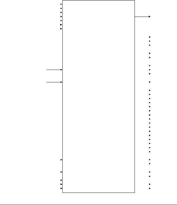
The PrimeCell Smart Card Interface (SCI) is an Advanced Microcontroller Bus Architecture (AMBA) compliant System-on-a-Chip (SoC) peripheral that is developed, tested and licensed by ARM. Refer to Figure 1-1 on page 1-3 for a block diagram of the SCI connections.
The PrimeCell SCI is an AMBA slave module that connects to the AMBA Advanced Peripheral Bus (APB), and interfaces to an external Smart Card reader. The SCI can autonomously control data transfer to and from the smart card. Transmit and receive data FIFOs are provided to reduce the required interaction between the CPU core or an AMBA Advanced High-performance Bus (AHB) master and the peripheral.
1-2 |
Copyright © 2001 ARM Limited. All rights reserved. |
ARM DDI 0228A |
Introduction
|
|
|
|
PRESETn |
|
|
|
|
|
|
|
|
|
PCLK |
|
|
|
|
|
APB |
|
|
|
PSEL |
|
|
|
||
|
|
|
|
|
interface |
|
|
|
PENABLE |
|
|
|||
inputs |
|
|
|
PWRITE |
|
|
|
|
|
|
|
|
|
PADDR[11:2] |
|
|
|
|
|
|
|
|
|
PWDATA[15:0] |
|
|
|
|
Card clock  SCICLKIN
Card data  SCIDATAIN
Card
SCIDETECT
detected
Hardware
card deactivate SCIDEACREQ request
SCI reset  nSCIRST
SCI clock  SCICLK
SCI Tx DMA |
|
SCITXDMACLR |
||
request clear |
|
|||
|
|
|||
SCI Rx DMA |
|
SCIRXDMACLR |
||
request clear |
|
|||
|
|
|||
|
|
|
|
SCANENABLE |
Scan test |
|
|
|
|
|
||||
interface |
|
|
|
SCANINPCLK |
|
||||
inputs |
|
|
|
SCANINSCICLK |
|
|
|
|
|
|
|
|
|
|
PrimeCell
SCI PL131
PRDATA[15:0]
APB interface output
nSCICLKOUTEN |
|
|
|
|
|
Card |
|
|
|
|
|
||
|
|
|
|
|
|
|
SCICLKOUT |
|
|
|
|
|
clock pad |
|
||||||
nSCICLKEN |
|
|
|
|
|
control |
|
|
|
|
|
Card |
|
nSCIDATAOUTEN |
|
|
|
|
|
|
|
|
|
|
|
||
|
|
|
|
|
||
|
|
|
|
|
data pad |
|
|
|
|
|
|
|
|
nSCIDATAEN |
|
|
|
|
|
control |
|
||||||
SCIVCCEN |
|
|
|
|
|
Card |
|
|
|
|
|
||
|
|
|
|
|
||
nSCICARDRST |
|
|
|
|
|
|
|
|
|
|
|
control |
|
|
|
|
|
|
||
|
|
|
|
|
|
|
SCIFCB |
|
|
|
|
|
|
|
|
|
|
|
|
|
SCIDEACACK |
|
|
|
|
Hardware |
|
|
|
|
|
card deactivate |
||
|
|
|
|
|||
|
|
|
|
|
||
|
|
|
|
|
acknowledge |
|
SCICARDININTR |
|
|
|
|
|
|
|
|
|
|
|
|
|
|
|
|
|
|
|
|
SCICARDOUTINTR |
|
|
|
|
|
|
|
|
|
|
|
|
|
SCICARDUPINTR |
|
|
|
|
|
|
|
|
|
|
|
|
|
SCICARDDNINTR |
|
|
|
|
|
|
|
|
|
|
|
|
|
SCITXERRINTR |
|
|
|
|
|
|
|
|
|
|
|
|
|
SCIATRSTOUTINTR |
|
|
|
|
|
|
|
|
|
|
|
|
|
SCIATRDTOUTINTR |
|
|
|
|
|
|
|
|
|
|
|
|
|
SCIBLKTOUTINTR |
|
|
|
|
|
SCI interrupts |
|
|
|
|
|
||
|
|
|
|
|
|
|
SCICHTOUTINTR |
|
|
|
|
|
|
|
|
|
|
|
|
|
SCIRTOUTINTR |
|
|
|
|
|
|
|
|
|
|
|
|
|
SCIRXTIDEOUTINTR |
|
|
|
|
|
|
|
|
|
|
|
|
|
SCITXTIDEOUTINTR |
|
|
|
|
|
|
|
|
|
|
|
|
|
SCIRORINTR |
|
|
|
|
|
|
|
|
|
|
|
|
|
SCICLKSTPINTR |
|
|
|
|
|
|
|
|
|
|
|
|
|
SCCLKACTINTR |
|
|
|
|
|
|
|
|
|
|
|
|
|
SCCINTR |
|
|
|
|
|
SCI Tx DMA |
|
|
|
|
|
||
SCITXDMASREQ |
|
|
|
|
|
|
|
|
|
|
|
||
|
|
|
|
|
||
|
||||||
|
|
|
|
|
service |
|
SCITXDMABREQ |
|
|
|
|
|
|
|
|
|
|
|
requests |
|
|
|
|
|
|
|
|
SCIRXDMASREQ |
|
|
|
|
|
SCI Rx DMA |
|
|
|
|
|
||
|
|
|
|
|
service |
|
SCIRXDMABREQ |
|
|
|
|
|
|
|
|
|
|
|
requests |
|
|
|
|
|
|
||
|
|
|
|
|
|
|
SCANOUTPCLK |
|
|
|
|
|
Scan test |
|
|
|
|
|
||
|
|
|
|
|
interface |
|
SCANOUTSCICLK |
|
|
|
|
|
|
|
|
|
|
|
outputs |
|
|
|
|
|
|
|
|
Figure 1-1 PrimeCell SCI connections
ARM DDI 0228A |
Copyright © 2001 ARM Limited. All rights reserved. |
1-3 |

Introduction
The features of the PrimeCell SCI are covered under the following headings:
•Features of the PrimeCell SCI on page 1-4
•Programmable parameters on page 1-5.
1.1.1Features of the PrimeCell SCI
The following features are provided by the PrimeCell SCI:
•Compliance to the AMBA Specification (Rev 2.0) onwards for easy integration into System-on-a-Chip (SoC) implementation.
•Supports asynchronous T0 and T1 transmission protocols.
•Supports clock rate conversion factor F = 372 or 512, with bit rate adjustment factors D = 1, 2, 4, 8, and 16 supported.
•Eight character deep buffered TX and RX paths.
•Direct interrupts for TX and RX FIFO level monitoring.
•Independent masking of all interrupts.
•Support for Direct Memory Access (DMA).
•Interrupt status register.
•Hardware initiated card deactivation sequence on detection of card removal.
•Software initiated card deactivation sequence on transaction complete.
•Limited support for synchronous smart cards through registered input/output.
•Identification registers that uniquely identify the PrimeCell SCI. These can be used by an operating system to automatically configure itself.
1-4 |
Copyright © 2001 ARM Limited. All rights reserved. |
ARM DDI 0228A |

Introduction
1.1.2Programmable parameters
The following key parameters are programmable:
•Smart Card clock frequency
•communication baud rate
•protocol convention
•card activation time
•card deactivation time
•check for maximum time for first character of Answer To Reset (ATR) reception
•check for maximum duration of ATR character stream
•check for maximum time for receipt of first character of data stream
•check for maximum time allowed between characters
•character guard time
•block guard time
•transmit character retry
•receive character retry
•transmit FIFO tide level
•receive FIFO tide level
•clock stop time
•clock start time
•clock inactive level.
Additional test registers and modes are implemented to provide efficient testing.
ARM DDI 0228A |
Copyright © 2001 ARM Limited. All rights reserved. |
1-5 |

Introduction
1-6 |
Copyright © 2001 ARM Limited. All rights reserved. |
ARM DDI 0228A |