- •Introduction
- •ARM7TDMI Architecture
- •The THUMB Concept
- •THUMB’s Advantages
- •ARM7TDMI Block Diagram
- •ARM7TDMI Core Diagram
- •ARM7TDMI Functional Diagram
- •Key to signal types
- •Processor Operating States
- •Switching State
- •Entering THUMB state
- •Entering ARM state
- •Memory Formats
- •Big endian format
- •Little endian format
- •Instruction Length
- •Data Types
- •Operating Modes
- •Registers
- •The ARM state register set
- •The THUMB state register set
- •The relationship between ARM and THUMB state registers
- •Accessing Hi registers in THUMB state
- •The Program Status Registers
- •The condition code flags
- •The control bits
- •Exceptions
- •Action on entering an exception
- •Action on leaving an exception
- •Exception entry/exit summary
- •Notes
- •Abort
- •Software interrupt
- •Undefined instruction
- •Exception vectors
- •Exception priorities
- •Not all exceptions can occur at once:
- •Interrupt Latencies
- •Reset
- •Instruction Set Summary
- •Format summary
- •Instruction summary
- •The Condition Field
- •Branch and Exchange (BX)
- •Instruction cycle times
- •Assembler syntax
- •Using R15 as an operand
- •Examples
- •Branch and Branch with Link (B, BL)
- •The link bit
- •Instruction cycle times
- •Assembler syntax
- •Examples
- •Data Processing
- •CPSR flags
- •Shifts
- •Instruction specified shift amount
- •Register specified shift amount
- •Immediate operand rotates
- •Writing to R15
- •Using R15 as an operand
- •TEQ, TST, CMP and CMN opcodes
- •Instruction cycle times
- •Assembler syntax
- •where:
- •Examples
- •PSR Transfer (MRS, MSR)
- •Operand restrictions
- •Reserved bits
- •Example
- •Instruction cycle times
- •Assembler syntax
- •Examples
- •Multiply and Multiply-Accumulate (MUL, MLA)
- •If the operands are interpreted as signed
- •If the operands are interpreted as unsigned
- •Operand restrictions
- •CPSR flags
- •Instruction cycle times
- •Assembler syntax
- •Examples
- •Multiply Long and Multiply-Accumulate Long (MULL,MLAL)
- •Operand restrictions
- •CPSR flags
- •Instruction cycle times
- •For signed instructions SMULL, SMLAL:
- •For unsigned instructions UMULL, UMLAL:
- •Assembler syntax
- •where:
- •Examples
- •Single Data Transfer (LDR, STR)
- •Offsets and auto-indexing
- •Shifted register offset
- •Bytes and words
- •Little endian configuration
- •Big endian configuration
- •Restriction on the use of base register
- •Example:
- •Data aborts
- •Instruction cycle times
- •Assembler syntax
- •Examples
- •Halfword and Signed Data Transfer(LDRH/STRH/LDRSB/LDRSH)
- •Offsets and auto-indexing
- •Halfword load and stores
- •Signed byte and halfword loads
- •Endianness and byte/halfword selection
- •Little endian configuration
- •Big endian configuration
- •Data aborts
- •Instruction cycle times
- •Assembler syntax
- •Examples
- •Block Data Transfer (LDM, STM)
- •The register list
- •Addressing modes
- •Address alignment
- •LDM with R15 in transfer list and S bit set (Mode changes)
- •STM with R15 in transfer list and S bit set (User bank transfer)
- •R15 not in list and S bit set (User bank transfer)
- •Use of R15 as the base
- •Inclusion of the base in the register list
- •Data aborts
- •Aborts during STM instructions
- •Aborts during LDM instructions
- •Instruction cycle times
- •Assembler syntax
- •Addressing mode names
- •Examples
- •Single Data Swap (SWP)
- •Bytes and words
- •Data aborts
- •Instruction cycle times
- •Assembler syntax
- •Examples
- •Software Interrupt (SWI)
- •Return from the supervisor
- •Comment field
- •Instruction cycle times
- •Assembler syntax
- •Examples
- •Supervisor code
- •Coprocessor Data Operations (CDP)
- •The coprocessor fields
- •Instruction cycle times
- •Assembler syntax
- •Examples
- •Coprocessor Data Transfers (LDC, STC)
- •The coprocessor fields
- •Addressing modes
- •Address alignment
- •Data aborts
- •Instruction cycle times
- •Assembler syntax
- •Examples
- •Coprocessor Register Transfers (MRC, MCR)
- •The coprocessor fields
- •Transfers to R15
- •Transfers from R15
- •Instruction cycle times
- •Assembler syntax
- •Examples
- •Undefined Instruction
- •Instruction cycle times
- •Assembler syntax
- •Instruction Set Examples
- •Using the conditional instructions
- •Using conditionals for logical OR
- •Absolute value
- •Multiplication by 4, 5 or 6 (run time)
- •Combining discrete and range tests
- •Division and remainder
- •Overflow detection in the ARM7TDMI
- •Pseudo-random binary sequence generator
- •Multiplication by constant using the barrel shifter
- •Multiplication by 2^n (1,2,4,8,16,32..)
- •Multiplication by 2^n+1 (3,5,9,17..)
- •Multiplication by 2^n-1 (3,7,15..)
- •Multiplication by 6
- •Multiply by 10 and add in extra number
- •General recursive method for Rb := Ra*C, C a constant:
- •Loading a word from an unknown alignment
- •Format Summary
- •Opcode Summary
- •Format 1: move shifted register
- •Operation
- •Instruction cycle times
- •Examples
- •Format 2: add/subtract
- •Operation
- •Instruction cycle times
- •Examples
- •Format 3: move/compare/add/subtract immediate
- •Operations
- •Instruction cycle times
- •Examples
- •Format 4: ALU operations
- •Operation
- •Instruction cycle times
- •Examples
- •Format 5: Hi register operations/branch exchange
- •Operation
- •Instruction cycle times
- •The BX instruction
- •Examples
- •Using R15 as an operand
- •Format 6: PC-relative load
- •Operation
- •Instruction cycle times
- •Examples
- •Format 7: load/store with register offset
- •Operation
- •Instruction cycle times
- •Examples
- •Format 8: load/store sign-extended byte/halfword
- •Operation
- •Instruction cycle times
- •Examples
- •Format 9: load/store with immediate offset
- •Operation
- •Instruction cycle times
- •Examples
- •Format 10: load/store halfword
- •Operation
- •Instruction cycle times
- •Examples
- •Format 11: SP-relative load/store
- •Operation
- •Instruction cycle times
- •Examples
- •Format 12: load address
- •Operation
- •Instruction cycle times
- •Examples
- •Format 13: add offset to Stack Pointer
- •Operation
- •Instruction cycle times
- •Examples
- •Format 14: push/pop registers
- •Operation
- •Instruction cycle times
- •Examples
- •Format 15: multiple load/store
- •Operation
- •Instruction cycle times
- •Examples
- •Format 16: conditional branch
- •Operation
- •Instruction cycle times
- •Examples
- •Format 17: software interrupt
- •Operation
- •Instruction cycle times
- •Examples
- •Format 18: unconditional branch
- •Operation
- •Examples
- •Format 19: long branch with link
- •Operation
- •Instruction cycle times
- •Examples
- •Instruction Set Examples
- •Multiplication by a constant using shifts and adds
- •General purpose signed divide
- •Thumb code
- •ARM code
- •Division by a constant
- •Explanation of divide-by-constant ARM code
- •ARM code
- •THUMB code
- •Overview
- •Cycle Types
- •Address Timing
- •Data Transfer Size
- •Instruction Fetch
- •Memory Management
- •Locked Operations
- •Stretching Access Times
- •The ARM Data Bus
- •The External Data Bus
- •The unidirectional data bus
- •The bidirectional data bus
- •Example system: The ARM7TDMI Testchip
- •Overview
- •Interface Signals
- •Coprocessor present/absent
- •Busy-waiting
- •Pipeline following
- •Data transfer cycles
- •Register Transfer Cycle
- •Privileged Instructions
- •Idempotency
- •Undefined Instructions
- •Debug Interface
- •Overview
- •Debug Systems
- •Debug Interface Signals
- •Entry into debug state
- •Entry into debug state on breakpoint
- •Entry into debug state on watchpoint
- •Entry into debug state on debug-request
- •Action of ARM7TDMI in debug state
- •Scan Chains and JTAG Interface
- •Scan limitations
- •Scan chain 0
- •Scan chain 1
- •Scan Chain 2
- •The JTAG state machine
- •Reset
- •Pullup Resistors
- •Instruction Register
- •Public Instructions
- •EXTEST (0000)
- •SCAN_N (0010)
- •INTEST (1100)
- •IDCODE (1110)
- •BYPASS (1111)
- •CLAMP (0101)
- •HIGHZ (0111)
- •CLAMPZ (1001)
- •SAMPLE/PRELOAD (0011)
- •RESTART (0100)
- •Test Data Registers
- •Bypass register
- •ARM7TDMI device identification (ID) code register
- •Operating mode:
- •Instruction register
- •Scan chain select register
- •Scan chains 0,1 and 2
- •Scan chain 0 and 1
- •Scan chain 0
- •Scan chain 1
- •Scan chain 3
- •ARM7TDMI Core Clocks
- •Clock switch during debug
- •Clock switch during test
- •Determining the Core and System State
- •Determining the core’s state
- •Determining system state
- •Exit from debug state
- •The PC’s Behaviour During Debug
- •Breakpoint
- •Watchpoints
- •Watchpoint with another exception
- •Debug request
- •System speed access
- •Summary of return address calculations
- •Priorities / Exceptions
- •Breakpoint with prefetch abort
- •Interrupts
- •Data aborts
- •Scan Interface Timing
- •Debug Timing
- •Overview
- •The Watchpoint Registers
- •Programming and reading watchpoint registers
- •Using the mask registers
- •The control registers
- •Programming Breakpoints
- •Hardware breakpoints:
- •Software breakpoints:
- •Hardware breakpoints
- •Software breakpoints
- •Setting the breakpoint
- •Clearing the breakpoint
- •Programming Watchpoints
- •The Debug Control Register
- •Debug Status Register
- •Coupling Breakpoints and Watchpoints
- •Example
- •CHAINOUT signal
- •RANGEOUT signal
- •Example
- •Disabling ICEBreaker
- •ICEBreaker Timing
- •Programming Restriction
- •Debug Communications Channel
- •Debug comms channel registers
- •Communications via the comms channel
- •Introduction
- •Branch and Branch with Link
- •THUMB Branch with Link
- •Branch and Exchange (BX)
- •Data Operations
- •Multiply and Multiply Accumulate
- •Load Register
- •Store Register
- •Load Multiple Registers
- •Store Multiple Registers
- •Data Swap
- •Software Interrupt and Exception Entry
- •Coprocessor Data Operation
- •Coprocessor Data Transfer (from memory to coprocessor)
- •Coprocessor Data Transfer (from coprocessor to memory)
- •Coprocessor Register Transfer (Load from coprocessor)
- •Coprocessor Register Transfer (Store to coprocessor)
- •Undefined Instructions and Coprocessor Absent
- •Unexecuted Instructions
- •Instruction Speed Summary
- •Timing Diagrams
ICEBreaker
The Watchpoint Registers
The two watchpoint units, known as Watchpoint 0 and Watchpoint 1, each contain three pairs of registers:
1.Address Value and Address Mask
2.Data Value and Data Mask
Table 39. Function and Mapping of ICEBreaker Registers
3. Control Value and Control Mask
Each register is independently programmable, and has its own address: see Table 39.
Address |
Width |
Function |
00000 |
3 |
Debug Control |
00001 |
5 |
Debug Status |
00100 |
6 |
Debug Comms Control Register |
00101 |
32 |
Debug Comms Data Register |
01000 |
32 |
Watchpoint 0 Address Value |
01001 |
32 |
Watchpoint 0 Address Mask |
01010 |
32 |
Watchpoint 0 Data Value |
01011 |
32 |
Watchpoint 0 Data Mask |
01100 |
9 |
Watchpoint 0 Control Value |
01101 |
8 |
Watchpoint 0 Control Mask |
10000 |
32 |
Watchpoint 1Address Value |
10001 |
32 |
Watchpoint 1 Address Mask |
10010 |
32 |
Watchpoint 1 Data Value |
10011 |
32 |
Watchpoint 1 Data Mask |
10100 |
9 |
Watchpoint 1 Control Value |
10101 |
8 |
Watchpoint 1 Control Mask |
165
Programming and reading watchpoint registers
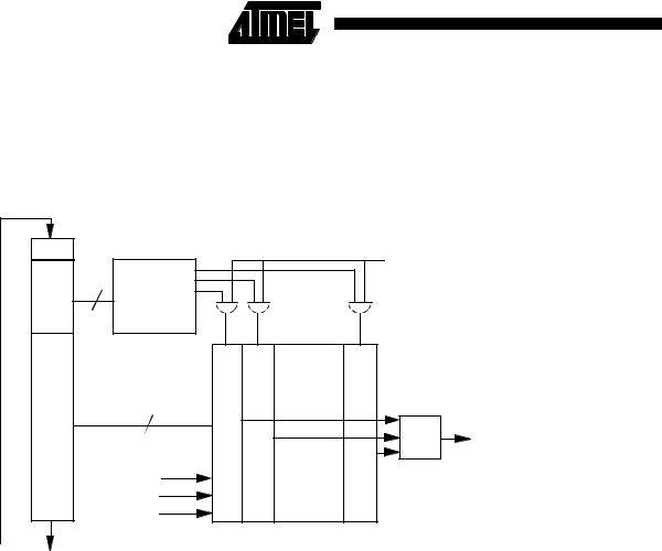
A register is programmed by scanning data into the ICEBreaker scan chain (scan chain 2). The scan chain consists of a 38-bit shift register comprising a 32-bit data field, a 5-
Figure 84. ICEBreaker Block Diagram
bit address field and a read/write bit. This is shown in Figure 84.
Scan Chain Register |
|
|
|
|
||
|
r/w |
|
|
|
Update |
|
|
4 |
|
|
|
|
|
|
|
|
|
|
|
|
|
|
Address |
|
|
|
|
|
Address |
Decoder |
|
|
|
|
|
0 |
|
|
|
|
|
|
31 |
|
|
|
|
|
|
|
32 |
|
|
|
|
|
Data |
|
|
|
+ |
BREAKPOINT |
|
|
|
|
|
||
|
|
A[31:0] |
Value |
Mask |
Comparator |
|
|
|
|
|
|
|
|
|
0 |
D[31:0] |
|
|
|
|
|
Control |
|
|
|
|
|
|
|
|
|
|
|
|
|
|
|
Watchpoint |
|
|
|
TDI |
TDO |
|
Registers and Comparators |
|
||
|
|
|
|
|
The data to be written is scanned into the 32-bit data field, the address of the register into the 5-bit address field and a 1 into the read/write bit.
A register is read by scanning its address into the address field and a 0 into the read/write bit. The 32-bit data field is ignored.
The register addresses are shown in Table 39.
Note: A read or write actually takes place when the TAP controller enters the UPDATE-DR state.
Setting the mask bit to 0 means that the comparator will only match if the input value matches the value programmed into the value register.
Using the mask registers
For each Value register in a register pair, there is a Mask register of the same format. Setting a bit to 1 in the Mask register has the effect of making the corresponding bit in the Value register disregarded in the comparison.
For example, if a watchpoint is required on a particular memory location but the data value is irrelevant, the Data Mask register can be programmed to 0xFFFFFFFF (all bits set to 1) to make the entire Data Bus field ignored.
Note: The mask is an XNOR mask rather than a conventional AND mask: when a mask bit is set to 1, the comparator for that bit position will always match, irrespective of the value register or the input value.
166 |
ICEBreaker |
|
|
||
|
The control registers
The Control Value and Control Mask registers are mapped identically in the lower eight bits, as shown below. Bit 8 of the control value register is the ENABLE bit, which cannot be masked.
Figure 85. Watchpoint Control Value and Mask Format
8 |
7 |
6 |
5 |
4 |
3 |
2 |
1 |
0 |
ENABLE |
RANGE |
CHAIN |
EXTERN |
nTRANS |
nOPC |
MAS[1] |
MAS[0] |
nRW |
|
|
|
|
|
|
|
|
|
The bits have the following functions:
nRW compares against the not read/write signal from the core in order to detect the direction of bus activity. nRW is 0 for a read cycle and 1 for a write cycle.
MAS[1:0] compares against the MAS[1:0] signal from the core in order to detect the size of bus activity.
The encoding is shown in the following table.
Table 40. MAS [1:0] Signal Encoding
bit 1 |
bit 0 |
Data size |
0 |
0 |
byte |
0 |
1 |
halfword |
1 |
0 |
word |
1 |
1 |
(reserved) |
nOPC is used to detect whether the current cycle is an instruction fetch (nOPC = 0) or a data access (nOPC = 1).
nTRANS compares against the not translate signal from the core in order to distinguish between User mode (nTRANS = 0) and non-User mode (nTRANS = 1) accesses.
ICEBreaker
EXTERN is an external input to ICEBreaker which allows the watchpoint to be dependent upon some external condition. The EXTERN input for Watchpoint 0 is labelled EXTERN0 and the EXTERN input for Watchpoint 1 is labelled EXTERN1.
CHAIN can be connected to the chain output of another watchpoint in order to implement, for example, debugger requests of the form “breakpoint on address YYY only when in process XXX”.
In the ARM7TDMI-ICEBreaker, the CHAINOUT output of Watchpoint 1 is connected to the CHAIN input of Watchpoint 0. The CHAINOUT output is derived from a latch; the address/control field comparator drives the write enable for the latch and the input to the latch is the value of the data field comparator. The CHAINOUT latch is cleared when the Control Value register is written or when nTRST is LOW.
RANGE can be connected to the range output of another watchpoint register. In the ARM7TDMI-ICEBreaker, the RANGEOUT output of Watchpoint 1 is connected to the RANGE input of Watchpoint 0. This allows the two watchpoints to be coupled for detecting conditions that occur simultaneously, eg for range-checking.
ENABLE If a watchpoint match occurs, the BREAKPT signal will only be asserted when the ENABLE bit is set. This bit only exists in the value register: it cannot be masked.
For each of the bits 8:0 in the Control Value register, there is a corresponding bit in the Control Mask register. This removes the dependency on particular signals.
167