

Chen Y.Resonant gate drive techniques for power MOSFETs
.pdf2.3 Loss Analysis
This section is to analyze the loss mechanism in driving a power MOSFET in this section. According to [II-1], the MOSFET gate drive loss consists of the following three parts: conduction loss, cross-conduction loss, and switching loss. Conduction loss refers to the power loss dissipated by the gate resistor Rg in Figure 2.1. Cross-conduction loss is caused by the “shoot-through” current going through both Q1 and Q2. Besides these two, there is a third type of loss involved. Whenever Q1 or Q2 switches, a crossover can be observed between the voltage and current of each switch. This crossover causes power loss, referred to as “switching loss” here. Among all three parts, conduction loss is usually the predominant part in driving a typical power MOSFET. Accordingly, it is analyzed first in this section.
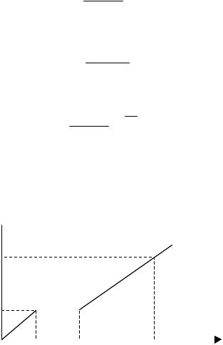
To determine the conduction loss accurately, current i in Figure 2.3a shall be first calculated, based on the gate charge-voltage waveform in Figure 2.2. For analysis convenience, Figure 2.2 is divided into three parts, as shown in Figure 2.6. These three parts stand for three different values of Cin. From time t0 to t1, when the gate charge Qg rises from 0 to Q1 and the gate voltage Vg rises from 0 to V1, the MOSFET gate capacitance is actually linear:
Cin _1 = Q1
V1
During this period, current i in Figure 2.3a drops exponentially:
t
i(t) =Vgate ×e−τ _ 1 Rg
where the time constant
τ _1=
1
Rg ×Cin_ 1
From time t1 to t2, Qg rises from Q1 capacitance during this period is
Cin _ 2
to Q2, but Vg does not rise.
=dQg = ¥ dVg
(2.3)
(2.4)
(2.5)
Therefore the gate
(2.6)
15
At this time period, i is also constant:
i(t) = Vgate −V1
Rg
From time t2 to t3, the relation between Vg and Qg is linear again. The gate capacitance is
Qgate - Q2
Cin _ 3 = Vgate -V1
At this period of time, i falls exponentially again:
t
i(t) =Vgate -V1 ×e−τ _ 3 Rg
where the time constant
(2.7)
(2.8)
(2.9)
τ _ 3 = |
|
1 |
(2.10) |
|
Rg |
×Cin _ 3 |
|||
|
|
Vg 
Vgate
V1 |
|
|
|
|
|
|
|
|
|
|
|
||
|
|
|
|
|
|
|
0(t0) Q1(t1) |
Q2(t2) |
Qgate(t3) |
Qg |
|||
|
Figure 2.6 |
Gate Capacitance at Dynamics |
|
|||
With above analysis, the current and voltage during charging period can again be plotted, as in Figure 2.7. As stated in Section 2.2, there is minor difference between the ideal waveforms in Figure 2.4 and the actual waveforms in Figure 2.7. Similarly, the actual current and voltage waveforms during discharging period can be plotted, as in Figure 2.8. Again, Figure 2.8 is not the same as Figure 2.5, in which the nonlinearity of Cin was not taken into consideration.
16

Vgate |
|
|
|
|
|
Vgate/Rg |
|
|
|
Vg |
|
|
|
|
|
||
|
|
|
|
i |
|
|
|
|
|
|
|
0 t1 |
t2 |
time |
|||
|
Figure 2.7 |
Actual Waveforms at Charging Period |
|
||
Vgate |
|
|
|
|
|
Vgate/Rg |
|
|
|
Vg |
|
|
|
|
|
||
|
|
|
i |
|
|
|
|
|
|
|
|
|
|
|
|
|
|
0 |
time |
Figure 2.8 Actual Waveforms at Discharging Period
With all waveforms in Figures 2.7 and 2.8, it is not difficult to find the conduction loss now. During the charging period, the total energy supplied by the voltage source Vgate is
∞ |
|
∞ |
|
|
ES = ò(Vgate ×i) ×dt = Vgate × ò(i × dt) = Vgate ×Qgate |
(2.11) |
|||
0 |
|
0 |
|
|
because the integral of current |
i over time is the total electric charge supplied into the |
|||
gate of the MOSFET. Meanwhile the energy stored by Cin is |
|
|
||
∞ |
t1 |
t 2 |
∞ |
|
EC = ò(Vg ×i) ×dt = ò(Vg ×i ×dt ) + ò(Vg ×i × dt) + ò(Vg ×i × dt) |
(2.12) |
|||
0 |
0 |
t1 |
t2 |
|
Given Equations 2.3 through 2.10, Equation 2.12 can be further solved:
t1 |
t1 |
|
|
dVg |
|
1 |
|
|
|
ò(Vg |
×i × dt) = ò(Vg |
×Cin _1 |
× |
) ×dt = |
×Q1 |
×V1 |
|||
dt |
2 |
||||||||
0 |
0 |
|
|
|
|
|
|||
|
|
|
|
|
|
|
17
|
|
|
|
|
t 2 |
|
|
|
|
|
|
|
|
t 2 |
|
|
|
|
|
|
|
|
|
|
|
|
|
|
|||
|
|
|
|
|
ò(Vg ×i × dt) = V1 × ò(i × dt) = (Q2 - Q1 ) ×V1 |
|
|
|
|
||||||||||||||||||||||
|
|
|
|
|
t1 |
|
|
|
|
|
|
|
|
t1 |
|
|
|
|
|
|
|
|
|
|
|
|
|
|
|||
t3 |
t3 |
|
|
|
|
dV |
|
|
|
1 |
|
Q |
|
|
|
- Q |
|
|
|
|
|
|
|
|
1 |
|
|
||||
ò(Vg |
×i × dt) = ò(Vg |
×Cin _ 3 × |
g |
) ×dt = |
× |
gate |
2 |
|
×(Vgate2 -V12 ) = |
(Qgate |
- Q2 )(Vgate + V1 ) |
||||||||||||||||||||
|
|
|
|
|
|
|
|
|
|
||||||||||||||||||||||
dt |
|
|
|
|
|
|
|
|
|
|
|
2 |
|||||||||||||||||||
t 2 |
t 2 |
|
|
|
|
|
|
|
2 Vgate - V1 |
|
|
|
|
|
|
|
|
||||||||||||||
|
E |
|
= |
1 |
Q V + (Q − Q )V + |
1 |
|
(Q |
|
|
|
− Q |
|
)(V |
|
|
+V ) |
(2.13) |
|||||||||||||
|
C |
|
|
gate |
2 |
gate |
|||||||||||||||||||||||||
|
|
|
2 |
1 |
1 |
|
2 |
|
1 |
1 |
|
2 |
|
|
|
|
|
1 |
|
|
|||||||||||
|
|
|
|
|
|
|
|
|
|
|
|
|
|
|
|
|
|
|
|
|
|
|
|
|
|
|
|
|
|||
It is |
important to |
realize |
that |
the |
expression in |
Equation |
2.13 |
|
is the |
area under the |
|||||||||||||||||||||
voltage-charge curve in Figure 2.6, as the shaded area redrawn in Figure 2.9. It is also obvious that Es is the area of the rectangle encircled by the two axis’s, Vgate and Qgate in Figure 2.9. Now with ES and EC, the energy dissipated by Rg can be found because of the conservation of energy:
Er _ ch arg ing = Es − Ec |
(2.14) |
which is the area left blank in Figure 2.9. It is worth mentioning that the MOSFET gate resistor Rg does not show in either Equation 2.11, or in Equation 2.13. In other words, for a given MOSFET, the value of Er_charging has nothing to do with the gate resistance Rg. This observation can ultimately lead to a conclusion that with conventional gate drive circuits, reducing gate resistance does not help reducing gate drive loss at all.
Vg |
|
|
Vgate |
|
|
0(t0) |
Qgate |
Qg |
Figure 2.9 |
Capacitor Energy at Charging Period |
|
By scaling ES to be unity, above energy distribution during charging period can also be depicted with a bar chart in Figure 2.10. Because of the “Miller Effect,” the relative heights between the EC bar and the Er_charging bar are very much dependant upon the gate
18
characteristic curve of a given power MOSFET as well as the current and voltage level the MOSFET is working at.
1 |
0.8 |
0.6 |
0.4 |
0.2 |
0 |

 Es
Es

 Ec
Ec

 Er_charging
Figure 2.10 Energy Distribution at Charging Period
The conduction loss at discharging period is much simpler than the charging period. At discharging period, all the previously stored energy EC is totally dissipated by Rg, regardless of the value of Rg:
Er _ discharg ing = Ec |
(2.15) |
And the energy distribution during this period can be plotted at in Figure 2.11.
1 |
0.8 |
0.6 |
0.4 |
0.2 |
0 |

 Ec
Ec

 Er_discharging
Figure 2.11 Energy Distribution at Discharging Period
Combining Equations 2.14 and 2.15, one can calculate the overall energy dissipation through a complete charging and discharging period:
Er = Er _ ch arg ing + Er _ discharg ing = ES = Qgate ×Vgate |
(2.16) |
19
Notice Qgate can also be expressed with Vgate and Cin by Equation 2.1, Equation 2.16 is equivalent to
Er = Cin ×Vgate2 |
|
(2.17) |
||||
Multiplied by the switching frequency fs, Equation |
2.17 leads to find the overall |
|||||
conduction loss in a conventional gate driver: |
|
|
|
|
||
P |
= C |
in |
×V 2 |
× f |
s |
(2.18) |
gd |
|
gate |
|
|
||
Compare Equation 2.18 with Equation 1.1; they are exactly the same. This equality somewhat reflects the statement at the very beginning of this chapter: conduction loss is usually the dominating part in overall gate drive loss.
Equation 2.18 concludes the conduction loss part of the overall gate drive loss in a conventional gate drive circuit. As stated before, conduction loss is the predominant part of the overall power loss, but not the only one. The overall MOSFET gate drive loss also consists of cross-conduction loss and switching loss. After conduction loss, it is now time to analyze cross-conduction loss and switching loss.
The cross-conduction loss in a conventional gate driver comes from the “shoot-through”
of Q1 and Q2 in Figure 2.1. Notice that in Figure 2.1 the gates of Q1 and Q2 share the same control signal Vtrig, which is a fairly common approach in industry to achieve fast
driving capability. However, there is an inherent problem associated with this
connection, caused by the practical waveform of Vtrig. The ideal waveform of the control signal Vtrig shall be of a pulse with infinitely steep rising and falling edges. However, in
reality that kind of ideal waveform is always not achievable, especially at high
frequencies. Inevitably there will be some distortion in the waveform. A comparison between an ideal Vtrig waveform and a real waveform is shown in Figure 2.12. During the rising edge of Vtrig, since the real waveform cannot be ideally steep, Q1 can be turned on before Q2 is totally turned off. During this short period of time, both Q1 and Q2 are on and there will be certain amount of current directly going out of the voltage source and
flowing through both driving |
MOSFETs. |
This phenomenon is called “shoot-through” in |
a conventional gate driver. |
During this |
“shoot-through” transition, the instantaneous |
power loss can be very high. |
|
|
20
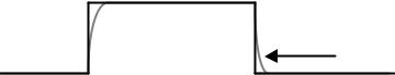
Ideal Vtrig 
Real Vtrig
Figure 2.12 Ideal and Real Waveforms of Control Signal
Same “shoot-through” can also happen during the falling edge of Vtrig, when Q2 is turned on before Q1 is totally turned off. Again there will be a current going through both Q1 and Q2 and causing a large amount of instantaneous power loss. The sum of both losses at rising and falling edges of Vtrig becomes the aforementioned cross-conduction loss. This is the second part of power loss in a conventional gate drive circuit.
The third part of power loss in a conventional gate driver is the switching loss. It mainly comes from the switching transitions of Q1 and Q2. During these transitions, the voltage across a MOSFET and the current through it overlap with each other. Since neither its voltage nor its current is negligibly low, there is a certain amount of power dissipated on the MOSFET. This part of power is referred as “switching loss.”
2.4 Summary
In this chapter, power loss in a conventional gate driver is analyzed. In driving a MOSFET, there are three types of losses involved: conduction loss, cross-conduction loss, and switching loss. Among these three, conduction loss dominates and this loss does not change when gate resistance changes. For the cross-conduction loss, several gate driver manufacturers have recently been seen applying separate control signals to Q1 and Q2 so that the aforementioned “shoot-through” problem can be avoided. However, by doing so, the gate driver may have some limitations for high frequency applications, where fast driving speed is a must. As to the last part of loss, switching loss, it is usually not significant unless in driving those power MOSFETs of large current and high voltage.
21
References:
[II-1] Boris S. Jacobson, “High Frequency Resonant Gate Driver with Partial Energy Recovery,” HFPC (High Frequency Power Conversion) Conference Proceedings, May 1993, pp. 133-141
[II-2] S. H. Weinberg, “A Novel Lossless Resonant MOSFET Driver”, IEEE PESC (Power Electronics Specialists Conference) Proceeding, 1992, pp. 1003-1010
[II-3] David A. Bell, Electronics Devices & Circuits, Second Edition, Reston Publishing Company, Inc., 1980
[II-4] Virginia Power Electronics Center (VPEC), Investigation of Power Management Issues for Next Generation microprocessors, Quarterly Progress Reports to VRM Consortium
22

Chapter III Resonant Gate Drive Techniques
With the preparation in Chapter II, it is now time to answer the question: How to reduce the gate drive loss? As stated in Chapter II, power loss in a conventional gate drive circuit consists of three parts, and among these three the conduction loss is the predominant part. Hence, if the conduction loss can be effectively reduced, the overall gate drive loss can also be expected to a noticeably lower level. Certainly, reducing cross-conduction loss and/or switching loss will also help, but that shall not be the main focus of research. The main focus is to reduce the conduction loss.
To reduce the conduction loss in a conventional gate driver, it is necessary to review the loss analysis in Section 2.3. In Section 2.3, Figures 2.10 and 2.11 depicted the energy distribution during charging and discharging periods, and Equation 2.18 described the total conduction loss. All these results, especially Figures 2.10 and 2.11, are very important, not only because they summarized the fundamental mechanism of conduction loss in a conventional gate driver, but also because they are of much use in deriving resonant gate drive techniques in this section. Hence Figures 2.10 and 2.11 are redrawn here as Figures 3.1 and 3.2. And the main focus in this chapter is to change the energy distribution in both figures so that less energy Er will be dissipated.
1 |
0.8 |
0.6 |
0.4 |
0.2 |
0 |

 Es
Es

 Ec
Ec

 Er_charging
Figure 3.1 Energy Distribution during Charging Period
23
1 |
0.8 |
0.6 |
0.4 |
0.2 |
0 |

 Ec
Ec

 Er_discharging
Figure 3.2 Energy Distribution during Discharging Period
3.1 Change Energy Distribution: Resonant Gate Drive
To change energy distribution in Figures 3.1 and 3.2 is equivalent to changing the heights of the energy bars in both figures. However some energy bars in both figures cannot be changed, such as ES and EC. ES corresponds the energy supplied by the voltage source. As long as the MOSFET needs Qgate amount of gate charge, following equation always stands:
∞ |
∞ |
|
ES = ò(Vgate ×i) ×dt = Vgate × ò(i × dt) = Vgate ×Qgate |
(3.1) |
|
0 |
0 |
|
Same is the situation of EC. As long as the MOSFET gate voltage is charged up from 0 to Vgate, Cin always stores EC amount of energy.
E |
|
= |
1 |
Q V + (Q − Q )V + |
1 |
(Q |
|
− Q |
)(V |
|
+V ) |
(3.2) |
C |
|
|
gate |
gate |
||||||||
|
|
2 |
1 1 2 1 1 |
2 |
|
2 |
|
1 |
|
|||
|
|
|
|
|
|
|
|
|
|
|
Given that both ES and EC cannot be changed, as well as that the conservation of energy must hold, it shall be clear that the only way to change the energy distribution in Figures 3.1 and 3.2 is to split the original Er-charging and Er_discharging bars into several fragments and to utilize some, if not all, of these fragments, instead to dissipate them all.
To split each Er bar in Figures 3.1 and 3.2 into fragments, it is not too circuitous to think of adding another component in series with the gate resistor Rg. Also, to recover some of these fragments, the additional component shall be of reactive instead of resistive.
24