

Chen Y.Resonant gate drive techniques for power MOSFETs
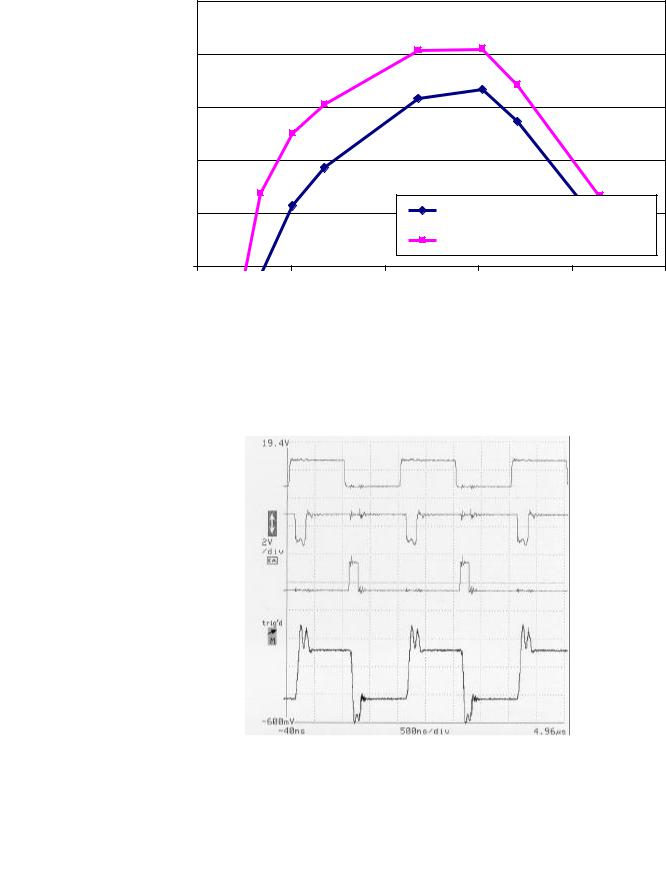
.pdfTo improve the efficiency of the Push-Pull Forward converter, the proposed resonant gate drive circuit was utilized to drive the MOSFETs in the secondary side and the experimental results are plotted in Figures 5.4 and 5.5. Figure 5.4 is the efficiency comparison at 300kHz; while Figure 5.5 is at 500kHz. From Figure 5.4, the proposed resonant gate driver can improve the overall efficiency by 1% at full load and 3% at half load, at 300kHz. At 500kHz, however, the resonant driver can improve more, as in Figure 5.5.
Efficiency Comparison at 300kHz
|
0.85 |
|
|
|
|
|
|
0.84 |
|
|
|
|
|
|
0.83 |
|
|
|
|
|
|
0.82 |
|
|
|
|
|
Efficiency |
0.81 |
|
|
|
|
|
0.8 |
|
|
|
|
|
|
0.79 |
|
|
|
|
|
|
|
|
|
|
|
|
|
|
0.78 |
|
|
|
|
|
|
0.77 |
|
|
w/ Conventional GD at secondary |
|
|
|
0.76 |
|
|
w/ Resonant GD at secondary |
|
|
|
0.75 |
|
|
|
|
|
|
10 |
20 |
30 |
40 |
50 |
60 |
Load Current (A)
Figure 5.4 Efficiency Comparison of a Push-Pull Forward Converter at 300kHz
55
Efficiency Comparison at 500kHz
|
0.8 |
|
|
|
|
|
|
0.78 |
|
|
|
|
|
Efficiency |
0.76 |
|
|
|
|
|
0.74 |
|
|
|
|
|
|
|
0.72 |
|
|
w/ Conventional GD at secondary |
|
|
|
|
|
|
w/ Resonant GD at secondary |
|
|
|
0.7 |
|
|
|
|
|
|
10 |
20 |
30 |
40 |
50 |
60 |
Load Current (A)
Figure 5.5 Efficiency Comparison of a Push-Pull Forward Converter at 500kHz
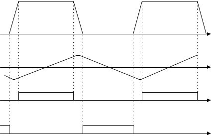
The experiment waveforms are also shown as in Figure 5.6.
Figure 5.6 Experiment Waveforms in Driving the Push-Pull Forward Converter
56

5.3 Comparison between Different Resonant Gate Drivers
As mentioned in Section 4.3, there have been other resonant gate drive circuits published in recent years to reduce the power loss in driving MOSFETs at high frequencies [V-4, 5, 6, 7, 8]. It is not complete for this thesis if it does not include these existing resonant gate drivers. However, most of the existing circuits are very complicated in circuitry, and use transformers in energy transfer, inherently limiting the driving speed (more on this in Chapter VI). Here in this section three typical circuits are introduced and the comparison between the proposed circuits and these two circuits will be made afterwards.
One of existing resonant gate drivers was published by Maksimovic in 1991 [V-5]. Its diagram is drawn in Figure 5.7 and its operation is illustrated in Fiugre 5.8. By
controlling the timing of |
Q1 and |
Q2, |
the |
circuit in Figure 5.7 uses the resonant inductor |
||||
Lr as |
a current source |
during |
both |
charging and discharging periods. Ideally (when |
||||
Rg=0), |
this circuit can be lossless, same |
as the proposed |
circuit; |
however, |
much worse |
|||
than the proposed circuit, this driver |
in |
Figure 5.7 has |
much |
conduction |
loss simply |
|||
because the current in Lr is continuously in resonance with Co and this current can not be small to drive the MOSFET. In other words, the driver in Figure 5.7 tradeoffs higher resonant conduction loss for lower gate conduction loss.
Vgate
Vd
|
|
Q1 |
|
|
|
Lr |
|
Ir |
Co |
Q2 |
Cin |
|
|
||
|
|
|
Figure 5.7 One Existing Resonant Gate Drive Circuit [V-5]
57
Vgs
t
Ix
t
Q1
t
Q2
t
Figure 5.8 Operation of the Resonant Gate Drive Circuit in Figure 5.7 [V-5]
Another drawback of the circuit in Figure 5.7 is that its Co and Lr, the only two additional components it adds to a conventional gate driver, have to be large in their value, as well as in their size. Not like the small inductor in the proposed circuit in Chapter IV, larger passive components are difficult in packaging and can make the whole gate driver bulky.
The third drawback of the circuit in Figure 5.7 is its transient performance. Since the capacitor Co has to be large enough to work as a voltage source, it needs pretty long time to reach a new stead-state when there occurs any change in duty cycle [V-7]. Therefore, its transient performance could be poor.
Another resonant gate driver to be introduced in this section is drawn in Figure 5.9. It was published by Jacobson in 1993 [V-4]. Basically this circuit tries to utilized the leakage inductors as the resonant inductor to achieve fast driving capability. Meanwhile it also tries to return some portion of inductor current back to the voltage source through the clamping diodes, so that some gate drive loss can be recovered. However, in experiment, the author of this circuit found a big discrepancy between the gate drive loss
58

measured from experiment and that from calculation [V-4]. He explained this discrepancy arising from the incorrectness of the calculation model [V-4].
Vgate
Q1 |
Vd |
|
Cin
Q2
Figure 5.9 Another Existing Resonant Gate Drive Circuit [V-4]
However, in my research, I found a serious problem with the circuit in Figure 5.9: the magnetic reset of the choke. Actually the inductor choke in Figure 5.9 cannot be reset unless the forward voltage drop across the clamping diodes are high enough. This result is shown in the simulation results in Figure 5.11 (the simulation circuit is drawn in Figure 5.10). When the diode forward drop is very low, or when the gate drive voltage is very high, or when the switching frequency is very high, the magnetic choke will not be reset and there will be big voltage spikes in the ends of the inductors. This result is also shown in Figure 5.12.
59

Figure 5.10 Simulation Model for the Circuit in Figure 5.9
Figure 5.11 Simulation Results with High Diode Voltage Drop
60
Figure 5.12 Simulation Results with Low Diode Voltage Drop
The third resonant gate driver to be included was invented by Weinburg [V-7]. Its circuit diagram is shown in Figure 5.13. The major drawback of this circuit is obviously its complexity. It also has speed problems because of the use of transformers (more on this in Chapter VI).
Figure 5.13 The Third Existing Resonant Gate Drive Circuit [V-7]
61
References:
[V-1] Vishay Siliconix, Si4410DY Datasheet, Revised on November 1998 [V-2] Homepage of Fluke Corporation, http://www.fluke.com
[V-3] Xunwei Zhou, Low-Voltage, High-Efficiency, Fast-Transient Voltage Regulator Module, Ph. D. Dissertation, Virginia Polytechnic Institute and State University, 1999
[V-4] Boris S. Jacobson, “High Frequency Resonant Gate Driver with Partial Energy Recovery,” HFPC (High Frequency Power Conversion) Conference Proceedings, May 1993, pp. 133-141
[V-5] Dragan Maksimovic, “A MOS Gate Drive with Resonant Transitions,” IEEE PESC (Power Electronics Specialists Conference) Proceeding, 1991, pp. 527-532 [V-6] Herman L. N. Wiegman, “A Resonant Pulse Gate Drive for High Frequency Applications,” IEEE APEC (Applied Power Electronics Conference) Proceeding,
1992, pp. 738-743
[V-7] S. H. Weinberg, “A Novel Lossless Resonant MOSFET Driver”, IEEE PESC (Power Electronics Specialists Conference) Proceeding, 1992, pp. 1003-1010
[V-8] J. Diaz, M. A. Perez, F. M. Linera, and F. Aldana, “A New Lossless Power MOSFET Driver Based on Simple DC/DC Converters,” IEEE PESC (Power Electronics Specialists Conference) Proceeding, 1995, pp. 37-43
62
Chapter VI
Half-Bridge MOSFET Gate Drive with Coupled Resonance
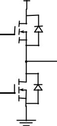
Power MOSFETs are widely used in the area of power electronics. They are seen as the essential elements in a tremendous number of applications, from PFC (Power Factor Correction) modules, to battery chargers, to DC/DC switching mode power supplies, etc. Generally speaking, a power MOSFET is utilized in two basic formats: a discrete switch or two MOSFETs connected together as shown in Figure 6.1. The latter format is often referred as the “Half-Bridge” configuration.
Figure 6.1 Half-Bridge Configuration
When two MOSFETs are connected in Half-Bridge, the gate drive for the top MOSFET is different from that for the bottom one. Since the source terminal of the top MOSFET is not grounded, it needs isolation at gate drive. In other words, the gate drive for the top MOSFET shall be floated as well. Currently there are three methods for this isolation: transformer isolation, optical coupler isolation, and bootstrap isolation. All these three methods are widely used.
However, none of above methods is perfect. The optical coupler method is very simple, but cannot work very fast at high frequency applications. The transformer method has
63

been in power electronic market for a long time, but has several drawbacks. First, a transformer is always bulky in a system; second, it has limit on the maximum duty cycle for magnetic reset; third, it has a lot of parasitics and at high frequency all these parasitics can affect the driving speed. For example, when all parasitics are considered, an ideal transformer like Figure 6.2a does not exist any more. Instead, it shall be modeled more accurately as Figure 6.2b. And because of all these parasitics, when a perfect gate drive pulse is applied at one side of a transformer, what can be observed from the other side of the transformer is strongly distorted. This distortion gets more serious at higher frequencies. Figure 6.3 shows a perfect gate drive pulse and the distorted one after a transformer.
(a) |
|
|
|
(b) |
|||||
Figure 6.2 |
Transformer Model: (a) an ideal transformer, and |
||||||||
|
(b) a practical transformer model with all parasitics included |
||||||||
|
|
|
|
|
|
|
|
|
|
|
|
|
|
|
|
|
|
|
|
|
|
|
|
|
|
|
|
|
|
|
|
|
|
|
|
|
|
|
|
Figure 6.3 Gate Drive Pulse Distortion by A Transformer
Because of all the above reasons, neither optical couplers nor transformers are used for high frequency gate drive isolations. In high frequency applications, people turn to the last resort: bootstrap isolation. Figure 6.4 illustrates a typical Half-Bridge MOSFET gate drive using bootstrap isolation. The right side with fine lines is the MOSFETs in HalfBridge construction; the left side of Figure 6.4 is the gate drive circuitry along with the controller (the block labeled with “Ctrl”). All gate drive circuits discussed in previous chapters go into the triangles in Figure 6.4. As in previous chapters, Vgate stands for the voltage source powering the whole gate drive circuitry.
64