

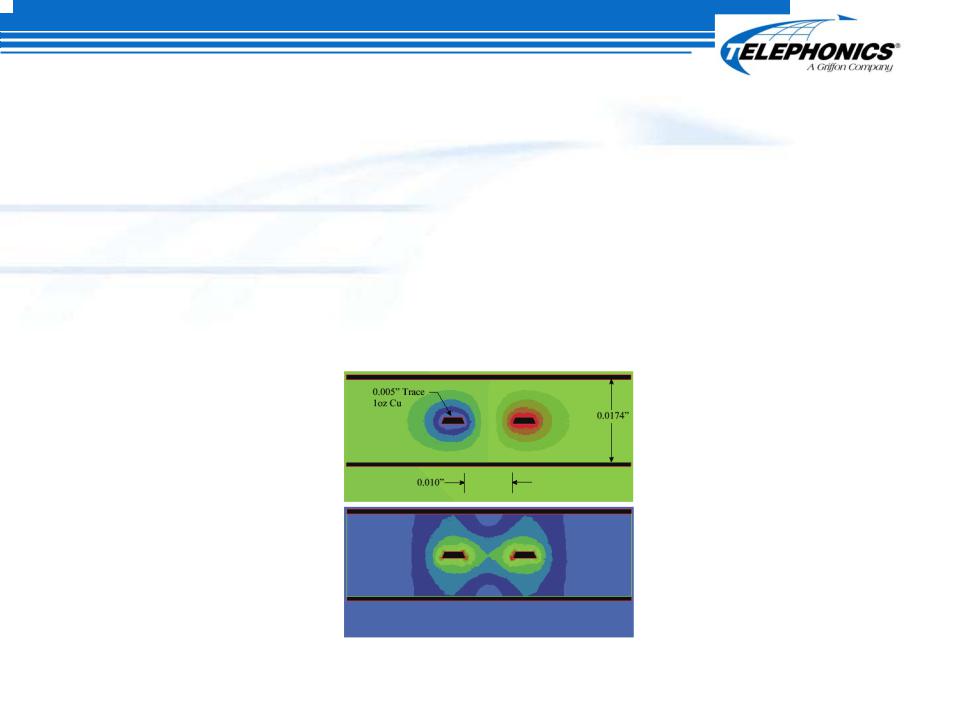
Field Intensity - 3
♦As the coupled lines are separated and/or the ground planes are brought closer, less of the electric field is concentrated between the conductors, and more of the field is concentrated between the ground planes and the conductors
Revision 4 |
Copyright Telephonics 2002-2005 |
51 |
|

Field Intensity - 4
♦When coupled lines are far apart, most of the electric field is concentrated between the ground planes and the conductors
- More ground return current
Revision 4 |
Copyright Telephonics 2002-2005 |
52 |
|

PWB Pad and Trace Parametersers
|
10 mil |
20 mil |
100 mil |
42 x 42 |
60 x 60 |
|
trace |
trace |
trace |
(≈ 0603) |
(≈ 0805) |
|
|
|
|
|
|
Capacitance |
2.2 pF/in |
3.3pF/in |
11.6pF/in |
0.24 pF |
0.45 pF |
|
|
|
|
|
|
Inductance |
9.9 nH/in |
7.2 nH/in |
2.4 nH/in |
0.19 nH |
0.21 nH |
|
|
|
|
|
|
Notes:
1.Copper: 1 oz, electrodeposited, strip-line.
2.FR4 dielectric constant: 4.50, loss tangent 0.025, height 10 mils.
Revision 4 |
Copyright Telephonics 2002-2005 |
53 |
|
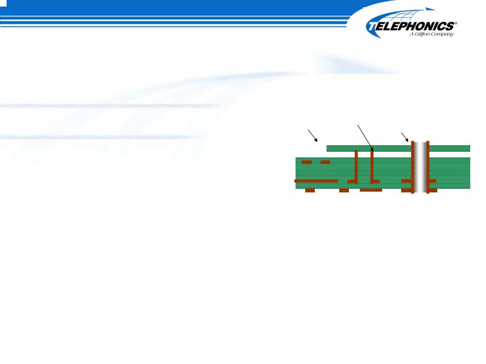
Vias
♦ Needed to interconnect layers
♦Minimize use
- Introduce discontinuities
Blind/Micro |
|
|
Buried Via |
|
Plated |
|
|
||||||||||||
Via |
|
|
|
|
|
|
|
|
|
Through Hole |
|
|
|||||||
|
|
|
|
|
|
|
|
|
|
|
|
|
|
|
|
|
|
|
|
|
|
|
|
|
|
|
|
|
|
|
|
|
|
|
|
|
|
|
|
|
|
|
|
|
|
|
|
|
|
|
|
|
|
|
|
|
|
|
|
|
|
|
|
|
|
|
|
|
|
|
|
|
|
|
|
|
|
|
|
|
|
|
|
|
|
|
|
|
|
|
|
|
|
|
|
|
|
|
|
|
|
|
|
|
|
|
|
|
|
|
|
|
|
|
|
|
|
|
|
|
|
|
|
|
|
|
|
|
|
|
|
|
|
|
|
|
|
|
|
(R, L, C)
- “Choke-off” routing
-Perforate Ground/Supply Planes
♦Traditionally implemented with Plated Through Holes (PTHs)
♦Consider Blind, Buried or Micro (4-6 mils) Vias
-Escape routing of high density components
-Additional processing cost can be offset by reduction in layers
Revision 4 |
Copyright Telephonics 2002-2005 |
54 |
|